

Page 1
CMOS LSI
Ordering number : EN*5219
22896HA (OT) No.5219-1/11
SANYO Electric Co.,Ltd. Semiconductor Bussiness Headquarters
TOKYO OFFICE Tokyo Bldg., 1-10, 1 Chome, Ueno, Taito-ku, TOKYO, 110-8534 JAPAN
1/5" Optical Size PAL Color
Solid-State Image Sensor
LC9998G
Overview
The LC9998G is a 1/5" optical size frame transfer type
CCD (charge-coupled device) solid-state image sensor
developed for use in color video cameras.
Features
• Effective number of pixels (total pixels): 499H × 582V
(532H × 600V)
• Number of optical black pixels:
Horizontal direction: Front: 7 pixels
Back: 26 pixels
Vertical direction: Front: 14 pixels
Back: 4 pixels
• Dummy bits: Horizontal direction: 4 pixels
• Horizontal resolution: 220 TV lines
• Supports miniature, compact camera designs.
• Package: 20-pin half-pitch transparent DIP
• Horizontal shift register: 5 V drive
• Supports variable-speed electronic shutter operation
Device Structure
• 1/5" type frame transfer CCD image sensor
• Unit cell size: 5.8 µm (H) × 3.75 µm (V)
• Chip size: 4.18 mm (H) × 5.10 mm (V)
• Parallel gate CCD sensor
• Built-in high-sensitivity output amplifier
• Cy-G-Ye stripe complementary color filter
Specifications
Absolute Maximum Ratings at Ta = 25°C, VSS= 0 V
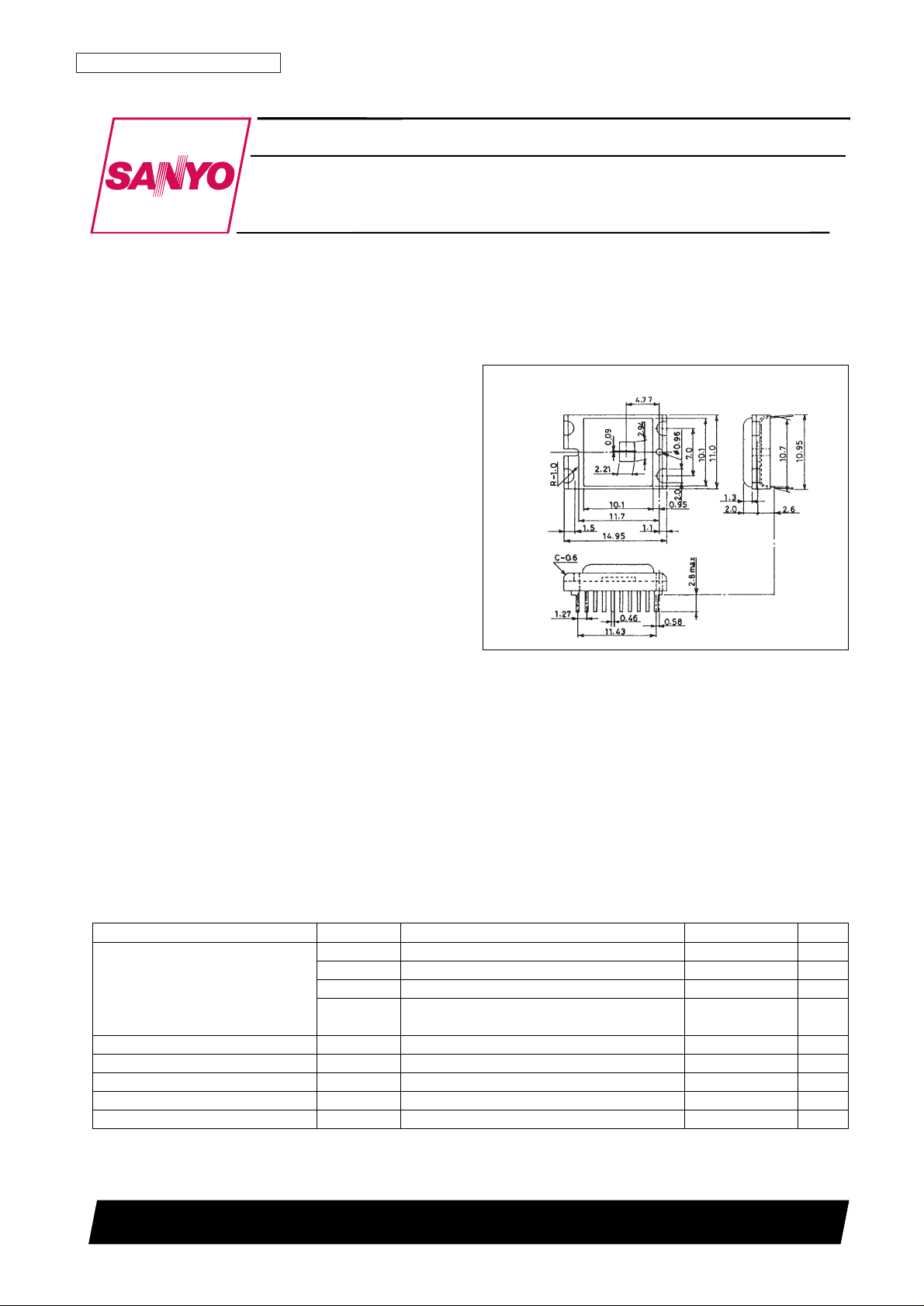
Package Dimensions
unit: mm
3217
Preliminary
[LC9998G]
Parameter Symbol Conditions Ratings Unit
V
DD
V
PW
= 0 V –0.3 to +18 V
V
GG
V
PW
= 0 V –0.3 to +5 V
Maximum supply voltage NSUB-PW –0.3 to +50 V
NSUB - ø1 to ø4,
–0.3 to +55 V
øS1 to øS4:
Horizontal clock pin øR V
PW
= 0 V –0.3 to +18 V
Other clock pins V
PW
= 0 V –15 to +18 V
Other pins V
PW
= 0 V –0.3 to +10 V
Operating temperature Topr –10 to +60 °C
Storage temperature Tstg –30 to +80 °C
Page 2
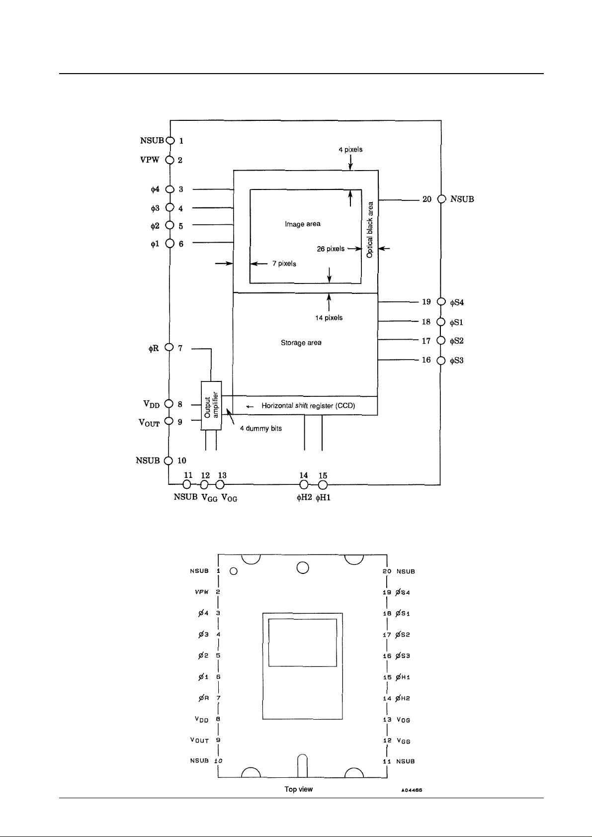
Block Diagram
Pin Assignment
No.5219-2/11
LC9998G
Page 3
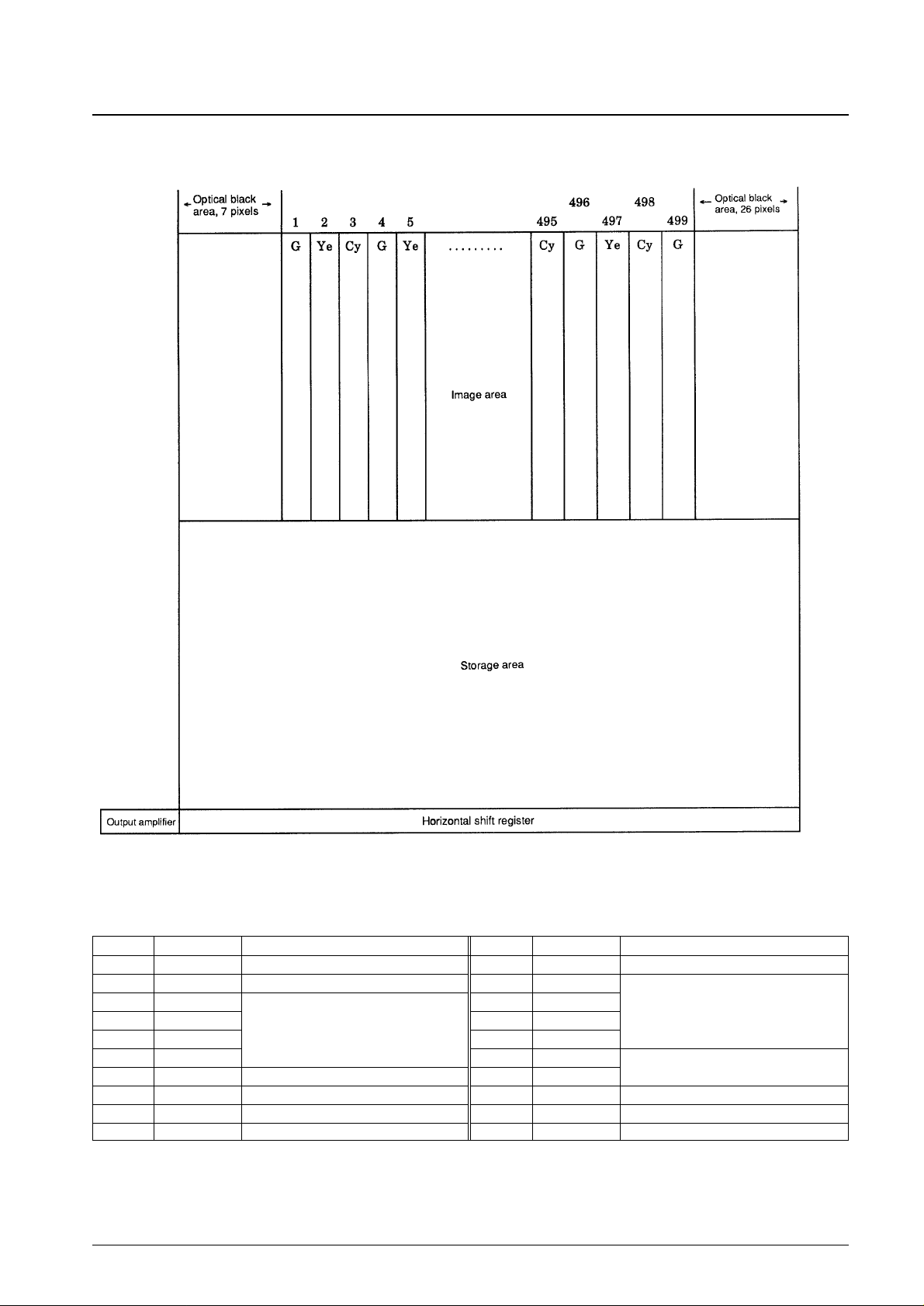
Pixel Arrangement
Pin Functions
No.5219-3/11
LC9998G
Pin No. Symbol Function Pin No. Symbol Function
1 NSUB N-substrate 20 NSUB N-substrate
2 VPW P-well 19 øS4
3 ø4 18 øS1
Storage area clock
4 ø3
Image area clock
17 øS2
5 ø2 16 øS3
6 ø1 15 øH1
Horizontal area clock
7 øR Reset gate 14 øH2
8 V
DD
Supply voltage 13 V
OG
CCD output gate
9 V
OUT
CCD output 12 V
GG
Load gate
10 NSUB N-substrate 11 NSUB N-substrate
Page 4
Specifications
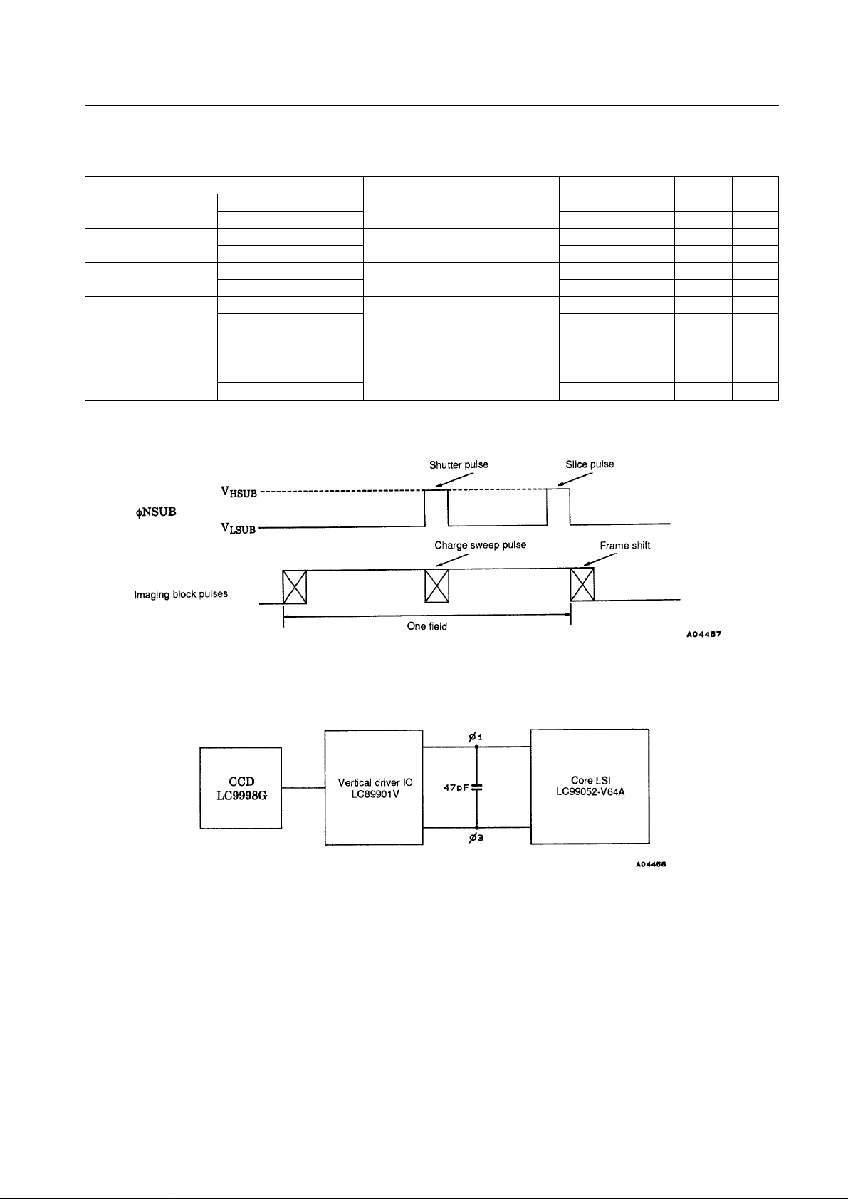
Clock Voltage Conditions at Frame frequency = 3.58 MHz
Note: 1. Insert 47 pF capacitors as shown in Figure 2.
2. Adjust V
HSUB
within the range where image degradation does not occur so that the saturated output level is maximized.
Figure 1
Figure 2
No.5219-4/11
LC9998G
Parameter Symbol Conditions min typ max Unit
Imaging block pulses
Pulse amplitude V
PIF
*1
14.0 14.5 15.0 V
ø1, ø2, ø3, ø4
Low level V
LIF
–10.0 –9.5 –9.0 V
Storage block pulses
Pulse amplitude V
PSL
14.0 14.5 15.0 V
øS1, øS2
Low level V
LSL
–7.0 –6.5 –6.0 V
Storage block pulses
Pulse amplitude V
PSL
14.0 14.5 15.0 V
øS3, øS4
Low level V
LSL
–8.0 –7.5 –7.0 V
Horizontal transfer pulses
Pulse amplitude V
PH
4.5 5.0 5.5 V
øH1, øH2
Low level V
LH
0 0 0.5 V
Reset gate
Pulse amplitude V
PR
4.5 5.0 5.5 V
øR
Low level V
LR
4.2 4.5 4.8 V
Substrate pulse
High level V
HSUB
*2
See Figure 1.
30.0 40.0 V
øNSUB
Low level V
LSUB
17.5 18.0 18.5 V
Page 5

Bias Conditions
Note: 1. Design applications so that this level never exceeds the substrate pulse low level V
LSUB
.
2. These are high-impedance inputs.
DC Characteristics
DC operating current
Note: VP: pulse amplitude
VL: low level
Figure 3 Pulse Waveform
No.5219-5/11
LC9998G
Parameter Symbol Conditions min typ max Unit
P-well V
PW
0 V
Output circuit voltage
V
DD
*1 14.5 15.0 15.5 V
V
GG
*2 1.2 1.5 1.8 V
OG bias V
OG
*2 4.5 5.0 5.5 V
Parameter Symbol Conditions min typ max Unit
DC operating current I
DD
4.5 7.0 11.0 mA
Symbol
t
WH
t
WL
t
r
t
f
Conditions Unit
typ typ typ typ
ø1 167 102 6.5 6.5
ø2 143 117 11 11
During frame drive
ns
ø3 167 102 6.5 6.5
When the frame shift frequency is 3.55 MHz
ø4 143 117 11 11
øS1 143 117 11 11
øS2 143 117 11 11
During frame drive
ns
øS3 143 117 11 11
When the frame shift frequency is 3.55 MHz
øS4 143 117 11 11
øS1 1.4 62.5 30 30
øS2 1.4 62.5 30 30
The values enclosed in dark lines are in µs units and apply
ns
øS3 62.5 1.4 30 30
during 1H line transfers.
øS4 62.5 1.4 30 30
øR 10 88 4 4 Reset pulse
øH1 50 50 3 3
During horizontal transfers
ns
øH2 50 50 3 3
øNSUB 9.9 19.99* 0.07 1 The slice pulse values marked * are in ms units. µs
øNSUB 4.2 19.99* 0.07 1 The shutter pulse values marked * are in ms units. µs
Page 6

Imaging Characteristics at Ta = 25°C
Note: 1. When the frame shift frequency is 3.55 MHz and the storage time is 1/50 second.
Test Procedures
The Sanyo evaluation board must be used for the following tests.
1. Sensitivity
Use a CCV31F pattern box (manufactured by Dai Nippon Printing Co., Ltd.) set up at a brightness of 1500 NT and
color temperature of 5100°K with no pattern. Image the pattern box with an HF16A lens (manufactured by Fujinon)
with a 1 mm thick C-500 IR cut filter in front of that lens.
Set the lens f-stop to f8 and set the lens to be 50 cm from the pattern box. Measure the CCD output signal from the
center of the image with this setup.
2. Uniformity of Output Signal
Measure under the following conditions.
• Standard drive conditions (See the specifications document.)
• Use a 3200°K color temperature halogen lamp as the light source.
• Use a 1 mm thick C-500 IR cut filter.
Set the CCD surface illumination to 7 lux, and divide the image into 45 areas as shown in Figure 4.
Measure the average value for each block, and determine the maximum, minimum, and mean of those values.
Determine the ratio of the range of the block average values to the mean of the block average values.
VF =
Figure 4
3. Saturated Signal
Saturate the output signal by removing the lens in the test setup for item 1. Measure the CCD output signal from the
center of the image in this state.
maximum block average value – minimum block average value
mean block average value
No.5219-6/11
LC9998G
Parameter Symbol Test method Conditions min typ max Unit
Sensitivity S 1 175 200 265 mV
Video signal imbalance VF 2 15 %
Saturated signal Vsat 3 500 mV
Smear SM 4 *1 0.04 %
Dark signal Vdrk 5 Ta = 55°C 7 mV
Color unevenness Vcs 6 40 mV
Gamma characteristics γ 1 —
Page 7

4. Smear
• Place a 1/10 V chart in front of the halogen light source as shown in the figure and image that chart.
• Adjust the amount of light entering the CCD with ND filters so that the CCD output signal at point A becomes
250 mV.
• Remove the ND filter(s) and measure the output value of the CCD output signal from the first line (point B).
SM = × 100 [%]
VB: The amount of smear at point B [mV]
TND: The ND filter transmissivity
Figure 5
5. Dark Signal
Completely block all light from falling on the CCD element surface and measure the CCD output signal at the center
of the image.
Here, do not measure the difference between this signal and the optical black section level, but rather measure the
difference between this signal and the no signal level that has no pixel information. (See Figure 6.)
Figure 6 Structure of a Single Horizontal Period
VB · TND
250
No.5219-7/11
LC9998G
Page 8

6. Color Uniformity
Use a CCV31F pattern box (manufactured by Dai Nippon Printing Co., Ltd.) set up at a brightness of 1500 NT and
color temperature of 5100°K with no pattern. Use the Sanyo LC9997-LE01 lens and a C-500 IR cut filter. Adjust the
exposure with ND filters so that the CCD output signal level is 500 mV. Measure the chrominance signal level and
chrominance signal phase at 16 points in the image as shown in Figure 7. Calculate the color unevenness, VCS(mV),
from these chrominance signal level and phase values.
BL =
RL =
BR =
RR =
VCS=
Figure 7
√
(BL – BR)2+ (RL – RR)
2
8
∑VR(i)SINθR(i)
i = 1
8
8
∑VR(i)COSθR(i)
i = 1
8
8
∑VL(i)SINθL(i)
i = 1
8
8
∑VL(i)COSθL(i)
i = 1
8
No.5219-8/11
LC9998G
VL, VR : Chroma level (mV)
θL, θR : Chroma level (˚)
Page 9

CCD Color Camera Block Diagram
Figure 8
Block Descriptions
No.5219-9/11
LC9998G
Block Product no. Specifications and functions
Vertical driver LC89901V
• Vertical CMOS driver
• Maximum frame transfer frequency: 3.55 MHz
• CMOS standard cell
• Built-in SSG (NTSC/PAL)
• Electronic iris circuit that supports even long exposure times
Image sensor core LSI LC99052-V64A
• Supports external image sensor drive control
• CDS and AGC early-stage signal-processing circuits
• Video bandwidth 8-bit A/D and D/A converters
• Supports mirror output
• Can also operate stand-alone
• Three channel 8-bit video signal inputs
• Three channel 8-bit video signal outputs
• Also functions as an RGB input encoder (NTSC/PAL)
Digital signal-
LC99062-W50 • Operates on HD, VD, and CLK inputs
processing LSI
• Simplified chrominance keying
• Superimpose
• Supports parameter setting in stand-alone mode
Page 10

Notes on Mounting and Handling
1. Preventing Electrostatic Discharge (ESD)
Since CCD sensors are easily destroyed by ESD, the antistatic measures described below should be employed when
handling this device.
• All tools and personnel must be grounded when handling CCDs. Note that a 1 MΩ resistor should be inserted in
series between personnel and ground for safety. (We recommend using wrist straps for personnel grounding.)
• Personnel should handle CCD devices with either bare hands or antistatic gloves. Use antistatic materials for work
garments. Personnel should wear conductive shoes.
• Lay conductive mats on the floor and benches in the workplace so that static charges do not accumulate.
• We recommend using ionized air blowers (or other static removal techniques) when handling CCD sensors.
• Use antistatic boxes when transporting boards that have CCD sensors mounted on them.
• Do not leave packing materials or fittings made from plastic materials (such as Styrofoam) that easily collect static
charges on or near workplace tables.
• Ground all tools, test equipment, conveyors, soldering irons, and other objects used in the workplace. Inspect
grounding regularly to assure that it is complete.
• Do not handle this IC in the vicinity of TV monitors or other equipment that generates high static voltages. If
unavoidable, install antistatic filters in front of monitor screens and take all other possible antistatic measures.
• Static charges accumulate easily in workplaces with a low relative humidity. Manufacturing operations should be
carried out in an environment with a relative humidity of at least 50%.
2. Soldering
• The CCD package temperature must not exceed 80°C.
• Since CCD sensors are sensitive to thermal stress as well as ESD, the soldering iron temperature should be under
300°C. Aim for a soldering time of 2 seconds per pin.
• Use soldering irons that include an adjustable temperature control function that holds the soldering iron tip at a
constant temperature.
• Be especially careful to assure that the device package temperature does not exceed 80°C when repairing or
redoing solder joints or when removing CCD sensors from printed circuit boards.
3. Soiling and Contamination Prevention
• CCD sensors should be handled in a clean workplace. (A class 1000 level is appropriate.)
• Do not touch the package surface and do not allow any object to contact the package surface. Use compressed air
to remove any foreign objects (such as dust) that land on the package surface. (We recommend using an ionized air
blower if possible.)
• Use a cotton swab dipped in ethyl alcohol to remove oily contamination, being especially careful not to scratch the
package surface.
• Use special-purpose cases to prevent soiling and contamination. Warm or cool CCD sensors in advance to prevent
condensation when transporting between rooms with radically differing temperatures.
• For CCD sensors that are shipped with protective tape applied, only remove that tape immediately prior to use in
an environment in which ESD prevention measures have been fully implemented. Do not reuse protective tape that
has been removed from a CCD sensor.
No.5219-10/11
LC9998G
Page 11

PS No.5219-11/11
LC9998G
4. Storage
• Do not allow sunlight or other bright light to fall on CCD sensors for extended periods.
• Since harsh conditions such as high temperatures or high humidities can adversely influence device characteristics,
do not use or store these devices in environments with such conditions. Samples should be stored in places where
the temperature and humidity fall in normal ranges, i.e., 5 to 35°C and 45 to 75% RH.
• Since CCD sensors are precision optical components, they should not be subjected to mechanical shocks.
• Avoid locations with corrosive atmospheres or high dust levels.
• Avoid locations subject to rapid temperature changes.
• Do not place heavy objects on top of boxes containing CCD sensors during storage.
• Use materials that cannot accumulate static charges for containers used to hold samples.
• Do not subject magazines holding CCD sensors to mechanical shocks, since this could adversely influence
reliability during mounting due to pin bending and other problems.
5. Notes on Mounting
• Flare can occur if a lens with an optical size larger than 1/5" is used. Consult your Sanyo sales representative in
advance when selecting lenses.
• This product is mounted in a fully transparent plastic package, and is easily influenced by light that passes through
the mounting board from the back to the front. Design end-products to adequately block out extraneous light.
6. Shipping
• Do not drop or throw packages containing CCD sensors.
• Do not allow packages containing CCD sensors to become wet due to rain or snow.
• Protect packages containing CCD sensors from mechanical shock and vibration as much as possible during
shipping.
This catalog provides information as of February, 1996. Specifications and information herein are subject to
change without notice.
■ No products described or contained herein are intended for use in surgical implants, life-support systems, aerospace
equipment, nuclear power control systems, vehicles, disaster/crime-prevention equipment and the like, the failure of
which may directly or indirectly cause injury, death or property loss.
■ Anyone purchasing any products described or contained herein for an above-mentioned use shall:
➀ Accept full responsibility and indemnify and defend SANYO ELECTRIC CO., LTD., its affiliates, subsidiaries and
distributors and all their officers and employees, jointly and severally, against any and all claims and litigation and all
damages, cost and expenses associated with such use:
➁ Not impose any responsibility for any fault or negligence which may be cited in any such claim or litigation on
SANYO ELECTRIC CO., LTD., its affiliates, subsidiaries and distributors or any of their officers and employees
jointly or severally.
■ Information (including circuit diagrams and circuit parameters) herein is for example only; it is not guaranteed for
volume production. SANYO believes information herein is accurate and reliable, but no guarantees are made or implied
regarding its use or any infringements of intellectual property rights or other rights of third parties.
 Loading...