

Page 1

Overview
The LC9997M is a 1/5-inch optical size frame transfer
CCD solid-state image sensor.
Features
• Effective pixels [total pixels]: 508 × 246 [532 × 250] (H
× V)
• Number of optical black pixels:
Horizontal:2 in front, 22 in back
Vertical: 2.5 above, 1.5 below
• Dummy bits: Horizontal: 4 pixels
• Horizontal resolution: 330 TV lines
• Small form factor supports compact application products
• 20-pin half-pitch transparent DIP package
• Horizontal shift register operates at 5 V.
• Supports variable-speed electronic shutter operation.
Device Structure
• 1/5-inch optical size frame transfer CCD image sensor
• Unit cell size: 5.8 µm ×9.0 µm (H × V)
• Chip size: 4.18 mm × 5.10 mm (H × V)
• Parallel gate CCD sensor
• Built-in high-sensitivity output amplifier
• Cy-G-Ye-W mosaic complementary color filters
Package Dimensions
unit: mm
3217
53098RM (OT) No. 5783-1/11
Preliminary
[LC9997M]
SANYO Electric Co.,Ltd. Semiconductor Bussiness Headquarters
TOKYO OFFICE Tokyo Bldg., 1-10, 1 Chome, Ueno, Taito-ku, TOKYO, 110-8534 JAPAN
1/5-Inch Frame Transfer CCD
NTSC Color Image Sensor
LC9997M
Ordering number : EN*5783
Parameter Symbol Conditions Ratings Unit
Supply voltage V
DD
VPW= 0 V –0.3 to +18 V
Load gate voltage V
GG
VPW= 0 V –0.3 to +5 V
N substrate - p-well voltage NSUB–VPW –0.3 to +50 V
N substrate - image and storage area voltage NSUB–
φ
1 to φ4, φS1 to φS4 –0.3 to +55 V
Horizontal clock pin,
φ
R: VPW= 0 V –0.3 to +18 V
Pin voltage Other clock pins: V
PW
= 0 V –15 to +18 V
Other pins: V
PW
= 0 V –0.3 to +10 V
Operating temperature Topr –10 to +60 °C
Storage temperature Tstg –30 to +80 °C
Specifications
Absolute Maximum Ratings at Ta = 25°C
Page 2
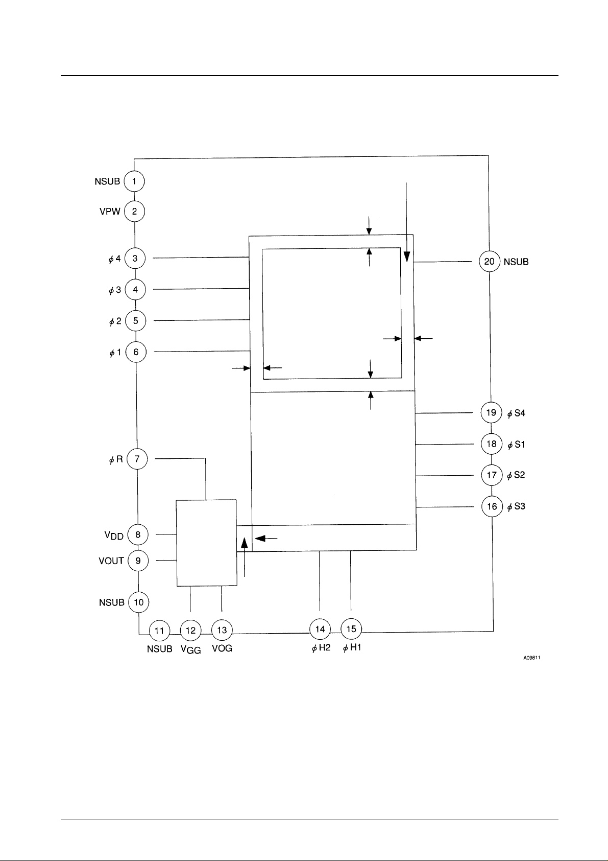
Block Diagram
No. 5783-2/11
LC9997M
Optical black area
1.5 pixels
Imaging area
2 pixels
22 pixels
2.5 pixels
Storage area
4 dummy bits
Output block
Horizontal shift register (CCD)
Page 3
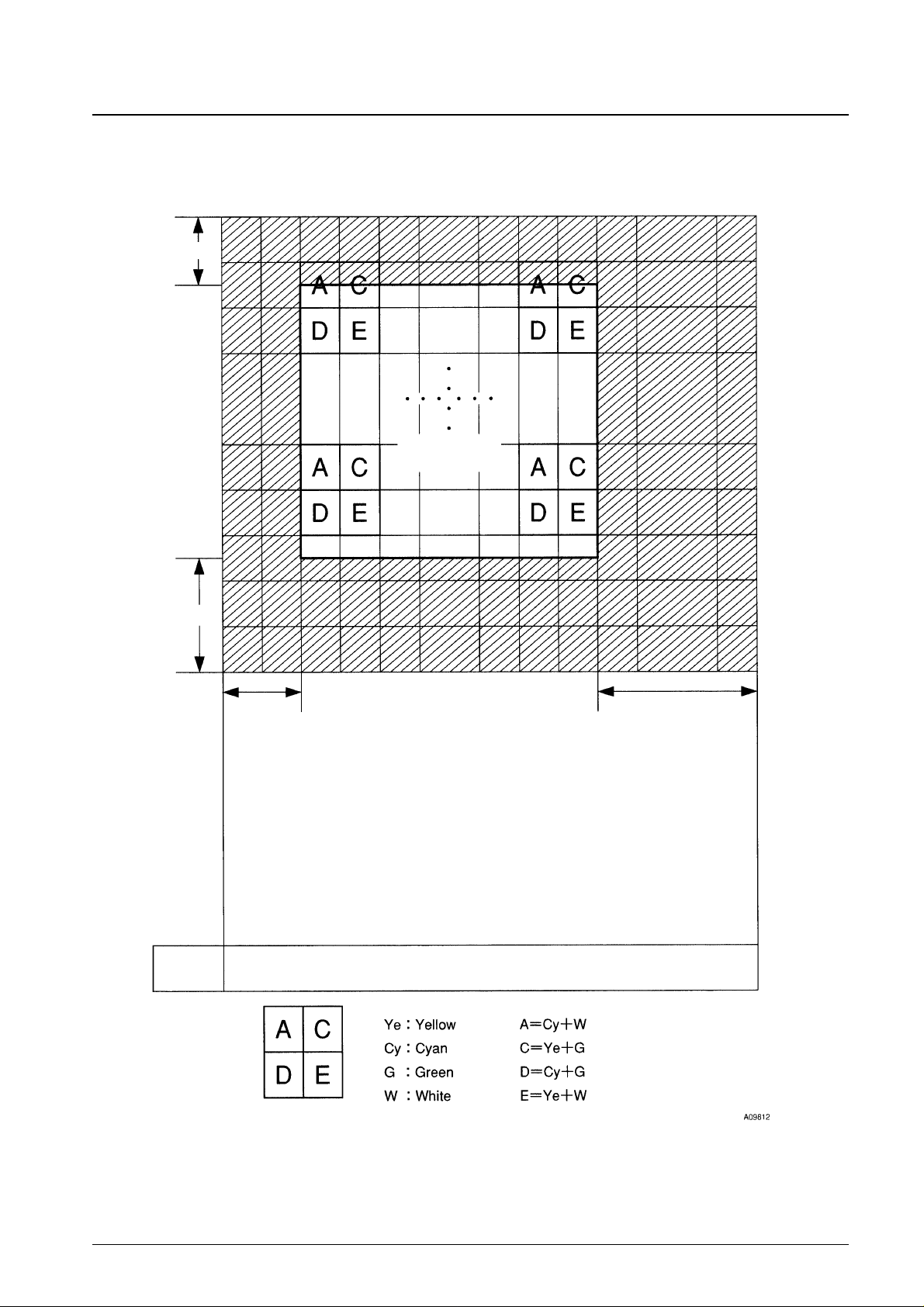
Pixel Arrangement
No. 5783-3/11
LC9997M
1.5 pixels
2.5 pixels
2 pixels
22 pixels
Imaging area
Storage area
Horizontal shift register
Output
amplifier
Page 4
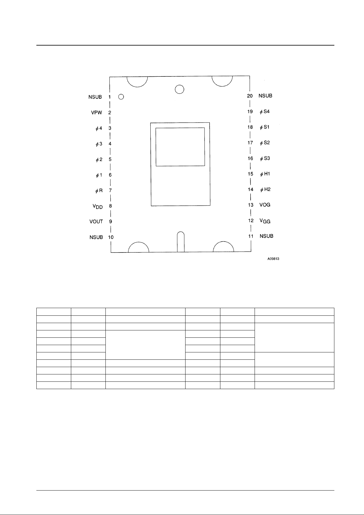
Pin Assignment
No. 5783-4/11
LC9997M
Pin Functions
Pin No. Symbol Function Pin No. Symbol Function
1 NSUB N substrate 20 NSUB N substrate
2 WPW P-well 19 φ S4
3 φ 4 18 φ S1
Storage area clocks
4 φ 3
Imaging area clock
17 φ S2
5 φ 2 16 φ S3
6 φ 1 15 φ H1
Horizontal block clocks
7 φR Reset gate 14 φ H2
8 V
DD
Supply voltage 13 V
OG
CCD output gate
9 V
OUT
CCD output 12 V
GG
Load gate
10 NSUB N substrate 11 NSUB N substrate
Page 5

No. 5783-5/11
LC9997M
Parameter Symbol Conditions
Ratings
Unit
min typ max
Imaging area pulse signals: ø1, ø2, ø3, ø4
Pulse amplitude V
PIF
*1 14.0 14.5 15.0 V
Low level V
LIF
*1 –10.0 –9.5 –9.0 V
Storage area pulse signals: øS1, øS2
Pulse amplitude V
PSL
14.0 14.5 15.0 V
Low level V
LSL
–8.0 –7.5 –7.0 V
Storage area pulse signals: øS3, øS4
Pulse amplitude V
PSL
14.0 14.5 15.0 V
Low level V
LSL
–9.0 –8.5 –8.0 V
Horizontal transfer pulse signals: øH1, øH2
Pulse amplitude V
PH
4.5 5.0 5.5 V
Low level V
LH
0 0 0.5 V
Reset gate: øR
Pulse amplitude V
PR
4.5 5.0 5.5 V
Low level V
LR
4.2 4.5 4.8 V
Substrate pulse: øNSUB
Pulse amplitude V
HSUB
*2. See Figure 1. 30.0 40.0 V
Low level V
LSUB
See Figure 1. 17.5 18.0 18.5 V
Clock Voltage Conditions at a frame shift frequency of 3.58 MHz
Notes: 1. Insert 47-pF capacitance as shown in Figure 2.
2. V
HSUB
must be adjusted so that the saturated output is maximum within the range where image degradation does not occur.
Figure 1
Figure 2
Parameter Symbol Conditions
Ratings
Unit
min typ max
P - well V
PW
0 V
Output circuit voltage
V
DD
*3 14.5 15.0 15.5 V
V
GG
*4 1.2 1.5 1.8 V
OG bias V
OG
*4 4.5 5.0 5.5 V
Bias Conditions
Shutter pulse
Slice pulse
Charge sweep-out pulse
One field
Frame shift
Imaging area pulses
Vertical driver IC
LC89901V
Core IC
LC99053
Page 6

Notes: 3. This voltage must not exceed the substrate pulse low level V
LSUB
.
4. These input pins are high-impedance inputs.
No. 5783-6/11
LC9997M
Parameter Symbol Conditions
Ratings
Unit
min typ max
DC operating current I
DD
4.5 7.0 11.0 mA
DC Characteristics
Drive Pulse Waveform Stipulations
Pulse Waveform Figure
Symbol
tWH tWL tr tf
Unit Notes
typ typ typ typ
φ
1 166 100 6.5 6.5
φ
2 141 116 11 11
ns
Frame transfer time
φ
3 166 100 6.5 6.5 When the frame shift frequency is 3.58 MHz
φ
4 141 116 11 11
φ
S1 141 116 11 11
φ
S2 141 116 11 11
ns
Frame transfer time
φ
S3 141 116 11 11 When the frame shift frequency is 3.58 MHz
φ
S4 141 116 11 11
φ
S1 1.36 62.1 30 30
φ
S2 1.36 62.1 30 30
ns
Vertical transfer time for a single horizontal line
φ
S3 62.1 1.36 30 30 Values in the box enclosed in the darker lines are in microseconds.
φ
S4 62.1 1.36 30 30
φ
R 11 86 4 4 Reset pulse
φ
H1 50 49 3 3 ns
Horizontal transfer time
φ
H2 50 49 3 3
φ
NSUB 9.9 16.59* 0.07 1 µs Slice pulse
φ
NSUB 4.2 16.59* 0.07 1 µs Shutter pulse
Parameter Symbol Conditions
Ratings
Unit
min typ max
[Sensitivity]
Luminance signal S Test method 1 130 mV
R gain G
R
Test method 1 0.7 2.4
B gain G
B
Test method 1 2.0 4.4
Image signal uninformity VF Test method 2 15 %
Saturation signal Vsat Test method 3, *5 600 mV
Smear SM Test method 4, *6 0.04 %
Dark signal Vdrk Test method 5. Ta = 55°C 7 mV
Color irregularity (mura) Vcs Test method 6 50 mV
Gamma characteristics γ 1
Imaging Characteristics (storage time = 1/60 s) at Ta = 25°C
Notes: 5. When the substrate pulse V
HSUB
is used fixed at 40±2 V, the minimum saturation output is 450 mV.
6. When the frame shift frequency is 3.58 MHz and the storage time is 1/60 s.
Note: The item marked with an asterisk (*) is in milliseconds.
VP: Pulse amplitude
VL: Low level
Page 7

Test Methods
The following tests are to be performed using the evaluation unit made by Sanyo Electric Co., Ltd.
1. Sensitivity
Using the CCD-SY1 light source (made by Wakasa Optical Co., Ltd.) illuminate the pixel surface with an intensity of
7 lux. Measure the CCD outputs (G, Ye, Cy, and W) at the center of the screen in that state with the T8331 tester
(made by Advantest, Inc.). The sensitivity is the average value for four pixels.
Use the following formulas to determined the R and G gains.
R = E – D
B = A – C
G = (C+D)/2
GR = G/R
GB = G/B
2.Image signal uniformity
Measure the uniformity under the following conditions
• The standard drive state (See the specifications document.)
• Using a halogen lamp with a color temperature of 3200 °K as the light source
• Using an IR cutting filter (C-500, 1mmt)
Illuminate the CCD surface with an intensity of 7 lux. Divide the surface of the CCD into 45 sections as shown in the
figure and measure the average value for each block. Determine the maximum, minimum, and mean of those
measurements, and determine the ratio of the difference with respect to the block average.
<Maximum of the block averages> – <Minimum of the block averages>
VF = ——————————————————————————————
<Mean of the block averages>
3. Saturation signal
Set up the following conditions using the Sanyo evaluation unit.
• The standard drive state (See the specifications document.)
• Light source: The LV-2001 pattern box (made by Kyoritsu Electronics, intensity: 870 NITS, color temperature:
3100 °K)
• Lens: HF 16A (made by Fujinon) with the aperture fully open.
Measure the CCD output signal from the center of the screen under these conditions.
4. Smear
• Place the 1/10-V chart described below in front of the halogen light source and image it.
• Using neutral density filters, adjust the incident illumination such that the CCD output signal at point A becomes
250 mV.
• Remove the neutral density filters and measure the value of the CCD output signal for the first line (i.e. at point B).
No. 5783-7/11
LC9997M
Page 8

VB · TND
SM = ————— × 100 [%]
250
VB: The amount of smear at point B (mV)
TND: The transmittance of the neutral density
filters used.
5. Dark signal
Block all light from the surface of the CCD element, and measure the CCD output signal at the center of the screen.
For this measurement, do not measure the difference between the signal level and the optical black area level, but
rather, read out the difference with the no-signal level at a point where there is no pixel information. (See the figure.)
Structure of the Horizontal Period
6. Color irregularity (mura)
With no pattern in the LV-2001 pattern box, image the pattern box with a C-500 1-mm thick IR cut filter and a 7%
neutral density filter over the whole surface of the 1/5-inch standard lens used for measurement. Verify that the CCD
average output at this time is over 200 mV. Calculate the color difference signals RY and BY from the following
formula from the average output of post-image processing R, G, and B signals. The color irregularity (mura) CS is
defined as the distance between the two points for which the data (RY and BY) is separated the most for all the areas.
RY = {(red-green) – (blue-green) × 0.25} × 101/64
BY = {(blue-green) – (red-green) × 0.125} × 50/64
CS = {(RY1-RY2)2+ (BY1-BY2)2}
1/2
Color Irregularity (mura) Data Acquisition Areas
No. 5783-8/11
LC9997M
Optical black area
Optical black area
Effective pixel area
No-signal area
In each block:
V direction: 30 pixels
H direction: 60 pixels
In each block:
V direction: 30 pixels
H direction: 60 pixels
Divided into 8 areas of equal separation.
Divided into 8 areas of equal separation.
Point A
Point B
Page 9

No. 5783-9/11
LC9997M
Image Defect Standards
Test Conditions
Defect position are classified on the monitor as shown below.
Test temperature Test item Allowable defects Notes
55°C White defects
At most 5 per zone
1
No white defects that cover 2 or more pixels in the horizontal direction or 2 or more lines in the vertical direction.
Black defects
At most 10 per zone
2
25°C No black defects that cover 2 or more pixels in the horizontal direction or 2 or more lines in the vertical direction.
Molding debris No defects 3
is not tested.
Notes
1. A white defect is a 10 mV or more higher than the CCD output optical black area for a black image. The CCD device is defective if any such level is 20
mV or more above the optical black level.
2. A black defect is a level that is 10% or more below the average level when the CCD is illuminated so that the average level is about 400 mV.
3. Using the Fujinon TV zoom lens H6 × 12.5R 1:1.2/12.5-75 stopped down to f 5.6 and with a 20% neutral density filter mounted, no dusts in the resin
should be visible on the image screen.
Page 10

Notes on Handling
1. ESD prevention
This CCD image sensor is easily damaged by ESD (electrostatic discharge). The following ESD prevention measures
must be taken when handling this device.
• All personnel and all equipment must be grounded when handling this CCD device. For safety, personnel should be
grounded through a resistor of about 1 MΩ. (We recommend using wrist straps.)
• This device should be handled with either bare hands or hands wearing antistatic gloves. Personnel should wear
antistatic clothing. Conductive shoes must be worn.
• Spread conductive mats on floors and benches in the work areas to prevent static charges from accumulating.
• We recommend using ionized air blowers to minimize static charges in areas where CCD sensors are handled.
• Antistatic boxes must be used for transporting substrate mounting materials.
• Packing materials, boxes, and other items made from plastics, such as styrofoam, that easily accumulate static
charges must not be placed on tables where CCD sensors are handled or in the vicinity of CCD handling operations.
• Tools, including testers, conveyors, and soldering irons, used in operations on CCD sensors must be grounded.
Furthermore, the quality of that grounding must be tested periodically.
• Do not handle this IC in the vicinity of TV monitors or other devices that generate high static charges. If
unavoidable, apply antistatic measures, such as covering the TV monitor screen with an antistatic filter.
• Since static charges accumulate more easily at a low relative humidity, the work environment must be maintained at
a relative humidity of 50% or higher.
2. Soldering
• The package temperature must not exceed 80°C.
• In addition to ESD, CCD sensors are easily damaged by thermal stress. When mounting on a printed circuit board,
the soldering iron temperature must never exceed 300°C, and the soldering time for each pin should be about 2
seconds.
• Only use soldering irons that include a temperature controller that holds the soldering tip at a fixed temperature.
• Be especially careful to avoid heating the device to over 80°C when repairing solder joints by hand and when
removing CCDs sensors from printed circuit boards.
3. Debris and contamination
• Handle CCD sensors in a clean location only.
• Do not touch the package surface with bare hands. Also, do not allow the package surface to come in contact with
any objects. If any foreign matter gets onto the package surface, remove it with an air blower. (We recommend
using an ionized air blower if possible.)
• Remove oil or grease contamination from the CCD package surface with a cotton swab dipped in ethyl alcohol. Be
careful not to damage the package surface.
• To prevent foreign matter and contamination from occurring, use dedicated cases to hold the CCD sensors, and also
equalize temperatures gradually when moving CCD sensors between rooms with radical temperature differences to
prevent condensation.
4. Storage
• Do not leave CCDs exposed to strong light, such as direct sunlight, for extended periods.
• Since high temperatures and high humidity can degrade device characteristics, avoid storing or using these devices
in such environments. The temperature and humidity of locations used to store samples must always be within
normal ranges (5 to 35°C and 45 to 75% RH).
• Since CCD sensors are precision optical instruments, be extremely careful not to apply mechanical shocks to these
devices.
• Avoid locations with corrosive atmospheres or high dust levels.
• Avoid locations subject to rapid temperature changes.
• Do not stack heavy objects on top of containers holding CCD sensors during storage.
• Containers used to hold sample must be made from materials with good antistatic properties.
• Be extremely careful not to apply mechanical shocks to these devices, since that could lead to bent pins and reduced
reliability during mounting.
No. 5783-10/11
LC9997M
Page 11

PS No. 5783-11/11
LC9997M
5. Notes on mounting
• Use of lenses with optical sizes in excess of 1/5 inch can lead to flare. Consult your Sanyo representative when
selecting lenses for use with this product.
• This product is mounted in a completely transparent plastic package, and thus is easily affected by light transmitted
from the back through the printed circuit board on which the device is mounted. Accordingly, applications must
provide adequate light shielding.
6. Transport
• Do not throw or drop packages containing CCD sensors.
• Protect CCD sensors from moisture when transporting during rain or snow.
• Minimize mechanical vibration and shock as much as possible when transporting CCD sensors.
This catalog provides information as of May, 1998. Specifications and information herein are subject to change
without notice.
■ No products described or contained herein are intended for use in surgical implants, life-support systems, aerospace
equipment, nuclear power control systems, vehicles, disaster/crime-prevention equipment and the like, the failure of
which may directly or indirectly cause injury, death or property loss.
■ Anyone purchasing any products described or contained herein for an above-mentioned use shall:
➀ Accept full responsibility and indemnify and defend SANYO ELECTRIC CO., LTD., its affiliates, subsidiaries and
distributors and all their officers and employees, jointly and severally, against any and all claims and litigation and all
damages, cost and expenses associated with such use:
➁ Not impose any responsibility for any fault or negligence which may be cited in any such claim or litigation on
SANYO ELECTRIC CO., LTD., its affiliates, subsidiaries and distributors or any of their officers and employees
jointly or severally.
■ Information (including circuit diagrams and circuit parameters) herein is for example only; it is not guaranteed for
volume production. SANYO believes information herein is accurate and reliable, but no guarantees are made or implied
regarding its use or any infringements of intellectual property rights or other rights of third parties.
 Loading...