

Page 1
Overview
The LC99063-LF2 is a color video signal processor for
use with the LC9997M/FL.
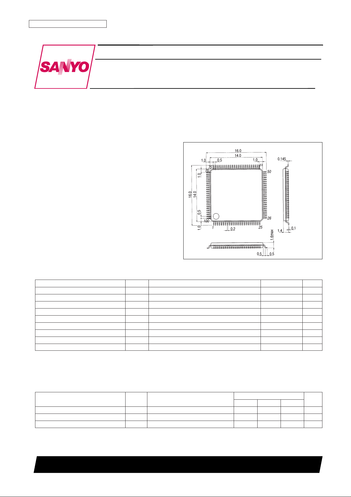
Package Dimensions
unit: mm
3181B-SQFP100
CMOS IC
51398RM (OT) No. 5787-1/8
SANYO: SQFP100
[LC99063-LF2]
SANYO Electric Co.,Ltd. Semiconductor Bussiness Headquarters
TOKYO OFFICE Tokyo Bldg., 1-10, 1 Chome, Ueno, Taito-ku, TOKYO, 110-8534 JAPAN
CCD Digital Signal Processing IC
LC99063-LF2
Ordering number : EN5787
Parameter Symbol Conditions Ratings Unit
Supply voltage V
DD
max –0.3 to +4.6 V
I/O voltage V
I
1, VOFor pin type 1 –0.3 to VDD+0.3 V
Input voltage V
I
2 For pin type 2 –0.3 to +7.3 V
Allowable power dissipation Pd max 400 mW
Operating temperature Topr –15 to +70 °C
Storage temperature Tstg –55 to +125 °C
Solder resistance (Hand soldering) 3s 350 °C
Solder resistance (Reflow) 10s 235 °C
I/O current Ii, Io * ±20 mA
Specifications
Absolute Maximum Ratings at VSS= 0 V
The pin types above refer to the following groups.
(1) DIN[32:9], DEVICE, MIRRO, SUPER, INMODE, WBHL, DOSL, SSET [2:1], OMODE [4:1], RES, DOUT [24:1], HREF, VDO, HDO, CLKOUT, ANA1,
ANA2, IREFOT1, IREFOT2, VREF1, VREF2, COMP1, COMP2
(2) DIN[8:1], CLK14M, CLK10M, HDI, VDI, HREF53, ENS, DATAS, CLKS, REGRES
*: This value is for a single I/O basic cell.
(1) DIN[32:9], DEVICE, MIRRO, SUPER, INMODE, WBHL, DOSL, SSET [2:1], OMODE [4:1], RES
(2) DIN[8:1], CLK14M, CLK10M, HDI, VDI, HREF53, ENS, DATAS, CLKS, REGRES
Parameter Symbol Conditions
Ratings
Unit
min typ max
Supply voltage V
DD
3 3.3 3.6 V
Input voltage range 1 Vin1 For pin type 1 0 V
DD
V
Input voltage range 2 Vin2 For pin type 2 0 +5.3 V
Allowable Operating Ranges at Ta = –15 to +70°C, VSS= 0 V
Page 2
LC99063-LF2
Parameter Symbol Conditions
Ratings
Unit
min typ max
Input high-level voltage V
IH
CMOS level ; for pin type 1 0.7 V
DD
V
Input low-level voltage V
IL
CMOS level ; for pin type 1 0.2 V
DD
V
Input high-level voltage V
IH
CMOS level with Schmitt ; for pin type 2 0.75 V
DD
V
Input low-level voltage V
IL
CMOS level with Schmitt ; for pin type 2 0.15 V
DD
V
Output high-level voltage V
OHIOH
= –2 mA; for pin types 3 and 4 VDD– 0.8 V
Output low-level voltage V
OLIOL
= +2 mA; for pin types 3 and 4 0.4 V
Input leak current I
L
VI= VDD; for pin types 1 and 2 –10 +10 µA
Output leak current Ioz High-impedance output; for pin type 3 –10 +10 µA
Electrical Characteristics for Logic Circuits
DC Characteristics at Ta = –15 to +70°C, VDD= 3.0 to 3.6 V, VSS= 0 V
The pin types above refer to the following groups.
INPUT
(1) DIN [32:9], DEVICE, MIRRO, SUPER, INMODE, WBHL, DOSL, SSET [2:1], OMODE [4:1], RES
(2) DIN [8:1], CLK14M, CLK10M, HDI, VDI, HREF53, ENS, DATAS, CLKS, REGRES
OUTPUT
(3) DOUT [24:1]
(4) HREF, VDO, HDO, CLKOUT
Note: The ANA1, ANA2, IREFOT1, IREFOT2, VREF1, VREF2, COMP1, and COMP2 pins fall outside these DC characteristic specifications.
Electrical Characteristics for Analog Circuits
Recommended operating conditions for D/A converter
Parameter Symbol Conditions
Ratings
Unit
min typ max
Reference voltage VREF1/2 1.11 V
Analog output resistance Ra 200 Ω
Reference voltage resistance Ri Ra
× 4 Ω
Phase compensation capacitor Cc 0.1 µF
VREF capacitor Cv 0.1 µF
No. 5787-2/8
Page 3
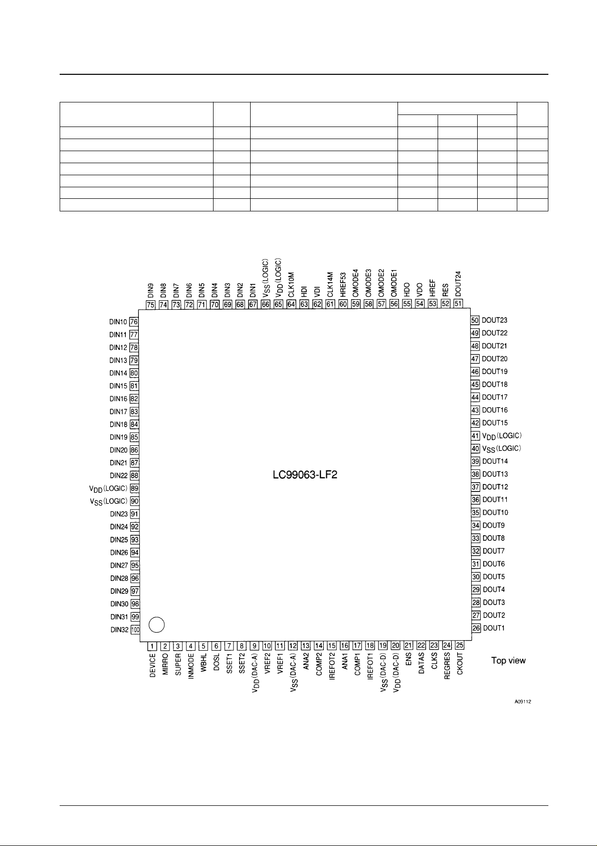
Pin Assignment
No. 5787-3/8
LC99063-LF2
Parameter Symbol Conditions
Ratings
Unit
min typ max
Resolution 8 Bits
Conversion frequency 15 MSPS
Zero scale output voltage –15 0 +15 mV
Full scale output voltage 1.01 1.1 1.19 V
Linearity error ±1.0 LSB
Differential linearity error ±0.5 LSB
Reference output voltage 1.09 1.1 1.11 V
Electrical Characteristics for D/A Converter at Ta = 25°C, VDD= 3.3 V, Rv = 200 Ω, Ri = 800 Ω
Page 4

No. 5787-4/8
LC99063-LF2
Pin Functions
Pin No. Symbol I/O Function
1 DEVICE I 0 : LC9997FL 1 : LC9997M
2 MIRRO I 0 : NORMAL 1 : MIRROR
3 SUPER I Superimpose control 0 : Superimpose 1 : Camera through
4 INMODE I Input mode select
5 WBHL I Auto white balance hold 0 : Hold 1 : Auto
6 DOSL I Pin 55 output select 0 : HD 1 : C.SYNC
7 SSET1 I Color sampling phase select
8 SSET2 I Color sampling phase select
9 V
DD
(DAC-A) P
10 VREF2 O DAC2 reference voltage output
11 VREF1 O DAC1 reference voltage output
12 V
SS
(DAC-A) P
13 ANA2 O DAC2 output
14 COMP2 I DAC2 bias pin
15 IREFOT2 O DAC2 reference current
16 ANA1 O DAC1 output
17 COMP1 I DAC1 bias pin
18 IREFOT1 O DAC1 reference current
19 V
SS
(DAC-D) P
20 V
DD
(DAC-D) P
21 ENS I Serial resister enable
22 DATAS B Serial resister data
23 CLKS I Serial resister CLK
24 REGRES I Serial resister reset
25 CKOUT O CCIR601, square PIX mode CLK
26 DOUT1 O Output Channel1 = CH1 (LSB)
27 DOUT2 O Output Channel1
28 DOUT3 O Output Channel1
29 DOUT4 O Output Channel1
30 DOUT5 O Output Channel1
31 DOUT6 O Output Channel1
32 DOUT7 O Output Channel1
33 DOUT8 O Output Channel1 = CH1 (MSB)
34 DOUT9 O Output Channel2 = CH2 (LSB)
35 DOUT10 O Output Channel2
36 DOUT11 O Output Channel2
37 DOUT12 O Output Channel2
38 DOUT13 O Output Channel2
39 DOUT14 O Output Channel2
40 V
SS
(logic)
41 V
DD
(logic)
42 DOUT15 O Output Channel2
43 DOUT16 O Output Channel2 = CH2 (MSB)
44 DOUT17 O Output Channel3 = CH3 (LSB)
45 DOUT18 O Output Channel3
46 DOUT19 O Output Channel3
47 DOUT20 O Output Channel3
48 DOUT21 O Output Channel3
49 DOUT22 O Output Channel3
50 DOUT23 O Output Channel3
51 DOUT24 O Output Channel3 = CH3 (MSB)
52 RES I 0 : Test 1 : Real
53 HREF O Horizontal reference
54 VDO O VD output
55 HDO O HD or C.SYNC output
Continued on next page.
Page 5

No. 5787-5/8
LC99063-LF2
Pin No. Symbol I/O Function
56 OMODE1 I
57 OMODE2 I
Output mode select
58 OMODE3 I
59 OMODE4 I
60 HREF53 I Horizontal reference (from LC99053)
61 CLK14M I
FSC4 (LC99053 pin 58), VD (LC99053 pin 56), HD (LC99053 pin 55)
62 VDI I
or HTCLK (LC99053 pin 51), fixed at high level, C.SYNC (LC99053 pin 54)
63 HDI I
64 CLK14M I HTCLK (LC99053 pin 51)
65 V
DD
(logic) P
66 V
SS
(logic) P
67 DIN1 I 8 bit data input (from LC99053) [LSB]
68 DIN2 I 8 bit data input
69 DIN3 I 8 bit data input
70 DIN4 I 8 bit data input
71 DIN5 I 8 bit data input
72 DIN6 I 8 bit data input
73 DIN7 I 8 bit data input
74 DIN8 I 8 bit data input (from LC99053) [MSB]
75 DIN9 I 8 bit Y input [LSB]
76 DIN10 I 8 bit Yinput
77 DIN11 I 8 bit Y input
78 DIN12 I 8 bit Y input
79 DIN13 I 8 bit Y input
80 DIN14 I 8 bit Y input
81 DIN15 I 8 bit Y input
82 DIN16 I 8 bit Y input [MSB]
83 DIN17 I 8 bit U or UV input [LSB]
84 DIN18 I 8 bit U or UV input
85 DIN19 I 8 bit U or UV input
86 DIN20 I 8 bit U or UV input
87 DIN21 I 8 bit U or UV input
88 DIN22 I 8 bit U or UV input
89 V
DD
(logic) P
90 V
SS
(logic) P
91 DIN23 I 8 bit U or UV input
92 DIN24 I 8 bit U or UV input [MSB]
93 DIN25 I 8 bit V input [LSB]
94 DIN26 I 8 bit V input
95 DIN27 I 8 bit V input
96 DIN28 I 8 bit V input
97 DIN29 I 8 bit V input
98 DIN30 I 8 bit V input
99 DIN31 I 8 bit V input
100 DIN32 I 8 bit V input [MSB]
Continued from preceding page.
Page 6

Block Diagram
No. 5787-6/8
LC99063-LF2
Page 7

No. 5787-7/8
LC99063-LF2
Major Functions
Luminance (Y) signal processing
• This block includes an 11-tap low pass filter.
• This block includes a gamma correction circuit using a five-segment curve with user-specified data points.
• This block provides vertical and horizontal outline enhancement with user-specified gain and coreling.
• This block includes a circuit for generating the 1.5× oversampling frequency.
Chrominance (U.V, U/V) signal processing
• This block uses a 9-tap low pass filter and color matrices to convert YUV input to an RGB signal.
• This block includes an auto white balance subblock.
— This subblock contains all circuits necessary for automatic white balance adjustment.
— This subblock offers a choice of automatic or manual operation.
— This subblock supports holding of automatic operation results.
— This subblock offers a choice of seven patterns—one for skin tones, for example.
• This block includes a gamma correction circuit using a three-segment curve.
• This block uses adjustable linear matrices to convert the color difference signals.
• This block includes an adjustable circuit for suppressing color noise at low luminance levels.
• This block includes an adjustable circuit for suppressing false-color signals occurring at edges and high-luminance
blocks.
• This block includes a circuit for generating the 1.5× oversampling frequency.
NTSC encoder
• This block encodes the RGB data using the timing from the HD, VD, and CLK (14.31818 MHz) input signals.
• This block supports color burst phase adjustment.
• The pedestal and burst levels are both adjustable.
I/O modes
• Input modes
— In addition to LC99053 output signals, the chip supports the Y, U, and V input configuration (Y.U.V) and the Y
and U/V one (Y.U/V).
— The chip can mix (superimpose) the signals from these two sources.
• Output modes
— Digital outputs: Digital composite video, digital Y.C, R.G.B, Y.U.V, and Y.U/V.
— Analog outputs using two 8-bit digital-to-analog converters: Composite video and Y.C
Other functions
• Registers are accessible via a 3-pin serial interface.
• The chip is capable of stand-alone operation.
• The chip supports mirror imaging (reversal of left and right).
• The chip supports pseudo interlacing.
• The chip supports negative imaging (creation of photographic negatives).
Important Notes
When used in combination with the LC99053-Z28, this chip supports the following modes with field periods longer than
1/60 second: extended exposure, M3, M4, and external ST and FT trigger. In these modes, however, the system requires
even more careful evaluation of circuit constants, trigger inputs, and other factors affecting CCD and driver operation.
Camera characteristics depend heavily on part layout and circuit design, so follow the guidelines set forth in
recommended circuit diagrams issued by Sanyo.
Page 8

PS No. 5787-8/8
LC99063-LF2
This catalog provides information as of May, 1998. Specifications and information herein are subject to change
without notice.
■ No products described or contained herein are intended for use in surgical implants, life-support systems, aerospace
equipment, nuclear power control systems, vehicles, disaster/crime-prevention equipment and the like, the failure of
which may directly or indirectly cause injury, death or property loss.
■ Anyone purchasing any products described or contained herein for an above-mentioned use shall:
➀ Accept full responsibility and indemnify and defend SANYO ELECTRIC CO., LTD., its affiliates, subsidiaries and
distributors and all their officers and employees, jointly and severally, against any and all claims and litigation and all
damages, cost and expenses associated with such use:
➁ Not impose any responsibility for any fault or negligence which may be cited in any such claim or litigation on
SANYO ELECTRIC CO., LTD., its affiliates, subsidiaries and distributors or any of their officers and employees
jointly or severally.
■ Information (including circuit diagrams and circuit parameters) herein is for example only; it is not guaranteed for
volume production. SANYO believes information herein is accurate and reliable, but no guarantees are made or implied
regarding its use or any infringements of intellectual property rights or other rights of third parties.
 Loading...