

Page 1
Ordering number : EN*5281A
22896HA (OT) No. 5281-1/6
Overview
The LC99012A-S is a timing generator for the 1/5-inch
LC9947G and LC9948G and the 1/6-inch LC9949G
black-and-white CCD image sensors.
Features
• 5 V single-voltage power supply
• Generates all pulses required for CCD drivers.
• Generates all pulses required for video signal
processing.
• Built-in synchronizing signal generator that supports
both EIA and CCIR.
• Includes buffer circuits for directly driving the CCD
horizontal transfer and reset gates.
• Includes light metering and control systems for an
automatic electronic iris function.
• Fixed rate-of-change control allows a smooth electronic
iris function to be implemented (an iris state output is
provided).
• Supports AGC control and a light metering mode that
compensates for backlighting.
• Selectable CCD storage mode (non-interlaced or
interlaced)
• Selectable TV scan mode (non-interlaced or interlaced)
• Allows all types of external synchronization.
• Built-in EXT-C.SYNC sync separator circuit
• Built-in phase comparator for external synchronization
• Control from external electronic shutter pulses and
frame shift pulses supports one-shot imaging.
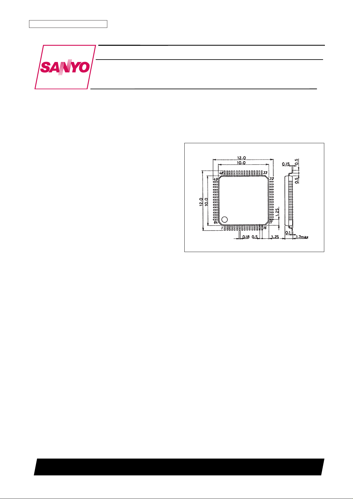
• Package: 0.5 mm lead pitch flat package (SQFP-64)
• Flickerless function
• Sensitivity-increasing function
Package Dimensions
unit: mm
3190-SQFP64
Preliminary
SANYO: SQFP64
[LC99012A-S]
LC99012A-S
SANYO Electric Co.,Ltd. Semiconductor Bussiness Headquarters
TOKYO OFFICE Tokyo Bldg., 1-10, 1 Chome, Ueno, Taito-ku, TOKYO, 110-8534 JAPAN
Black-and-White CCD Timing Generator
CMOS LSI
Page 2
Specifications
Absolute Maximum Ratings at VSS= 0 V
Note: * Per individual I/O reference cell
Allowable Operating Ranges at Ta = –30 to +65°C, VSS= 0 V
DC Characteristics: Input and Output Levels at VSS= 0 V, VDD= 4.5 to 5.5 V, Ta = –30 to +65°C
See the note on next page.
No. 5281-2/6
LC99012A-S
Parameter Symbol Conditions Ratings Unit
Maximum supply voltage V
DD
max –0.3 to +7.0 V
Input and output voltages V
I
, V
O
–0.3 to VDD+ 0.3 V
Allowable power dissipation Pd max Ta ≤ 65°C 290 mW
Operating temperature Topr –30 to +65 °C
Storage temperature Tstg –55 to +125 °C
Soldering heat resistance
Hand soldering: 3 seconds 350 °C
Reflow soldering: 10 seconds 235 °C
Input and output currents I
I
, I
O
±20* mA
Parameter Symbol Conditions min typ max Unit
Supply voltage V
DD
4.5 5.0 5.5 V
Input voltage range V
IN
0 V
DD
V
Parameter Symbol Conditions min typ max Unit
Input high-level voltage V
IH
1 TTL levels: (6) 2.2 V
Input low-level voltage V
IL
1 TTL levels: (6) 0.8 V
Input high-level voltage V
IH
2 CMOS levels: (1), (3) 0.7 V
DD
V
Input low-level voltage V
IL
2 CMOS levels: (1), (3) 0.3 V
DD
V
Input high-level voltage V
IH
3 CMOS levels, Schmitt inputs: (4) 0.8 V
DD
V
Input low-level voltage V
IL
3 CMOS levels, Schmitt inputs: (4) 0.2 V
DD
V
Input high-level voltage V
IH
4 CMOS levels, inputs with pull-up resistors: (2) 0.7 V
DD
V
Input low-level voltage V
IL
4 CMOS levels, inputs with pull-up resistors: (2) 0.3 V
DD
V
Input high-level voltage V
IH
5 CMOS levels, inputs with pull-up resistors: (5) 0.7 V
DD
V
Input low-level voltage V
IL
5 CMOS levels, inputs with pull-up resistors: (5) 0.3 V
DD
V
Output high-level voltage V
OH
1 IOH= –3 mA: (6), (13), (14), (15) VSS– 2.1 V
Output low-level voltage V
OL
1 IOL= 3 mA: (6), (13), (14), (15) 0.4 V
Output low-level voltage V
OL
2 IOL= 3 mA: (9) 0.4 V
Output high-level voltage V
OH
3 IOH= –6 mA: (12) VDD– 2.1 V
Output low-level voltage V
OL
3 IOL= 6 mA: (12) 0.4 V
Output high-level voltage V
OH
4 IOH= –6 mA: (7) VDD– 2.1 V
Output low-level voltage V
OL
4 IOL= 2 mA: (7) 0.4 V
Output high-level voltage V
OH
5 IOH= –30 mA: (11) VDD– 2.1 V
Output low-level voltage V
OL
5 IOL= 10 mA: (11) 0.4 V
Output high-level voltage V
OH
6 IOH= –12 mA: (8) VDD– 2.1 V
Output low-level voltage V
OL
6 IOL= 12 mA: (8) 0.4 V
Output high-level voltage V
OH
6 IOH= –12 mA: (10) VDD– 1.5 V
Output low-level voltage V
OL
7 IOL= 6 mA: (8) 0.4 V
Input leakage current I
IL
VI= VSS, VDD: (1), (3), (4), (6) –10 +10 µA
Output leakage current I
OZ
In high-impedance output mode: (6), (9), (13) –10 +10 µA
Pull-up resistance R
UP
(2) 10 20 40 kΩ
Pull-down resistance R
DN
(5) 25 50 100 kΩ
Page 3

Note: The applicable pin sets are defined as follows:
Input
(1) ......AI, CKI
(2) ......FLESS, STR, TEST
(3) ......EXT1, EXT2, KISYU, TV
(4) ......HR, SELMET1, SELMET2, VR
(5) ......CCDSCAN, EXT3, EXT4, MSENS, SENS, SSGSCAN
I/O
(6) ......STEPSTOP
Output
(7) ......PCO
(8) ......DHTR
(9) ......IRRES
(10) ....A0, CKO
(11) ....DHT1, DHT2
(12) ....DS1, DS2
(13) ....AGCC2, IRSTA
(14) ....CLK14M, CLP1, CLP2, FLD, HD, NSUB1, NSUB2, VD
(15) ....CBLK, C.SYNC, NSUB3, PBLK, VI1 to VI4, VS1 to VS4
* ......VIDI, VIDO, DCH, DCL, IRIS (These pins are not covered in the DC characteristics.)
Pin Assignment
I/O → I: Input pin, O: Output pin, B: Bidirectional pin, P: Power supply pin, NC: Unconnected pin
Note: All V
DD
and VSSpins must be connected to the power supply or ground. Do not leave any of these pins open.
No. 5281-3/6
LC99012A-S
No. Symbol I/O No. Symbol I/O
1 V
SS
P 64 DCL I
2 PCO O 63 DCH I
3 AI I 62 IRIS I
4 AO O 61 IRRES O
5 CKI I 60 VIDO O
6 CKO O 59 VIDI I
7 CCDSCAN I 58 IRSTA O
8 SSGSCAN I 57 AGCC2 O
9 CLK14M O 56 V
DD
P
10 HD O 55 TV I
11 VD O 54 C.SYNC O
12 FLD O 53 CBLK O
13 V
DD
P 52 PBLK O
14 KISYU I 51 CLP2 O
15 HR I 50 CLP1 O
16 VR I 49 V
SS
P
17 V
SS
P 48 DS1 O
18 SELMET1 I 47 DS2 O
19 SELMET2 I 46 V
DD
P
20 EXT1 I 45 DHT2 O
21 EXT2 I 44 DHT1 O
22 EXT3 I 43 DHTR O
23 EXT4 I 42 V
SS
P
24 V
DD
P 41 VS3 O
25 STEPSTOP B 40 VS2 O
26 SENS I 39 VS1 O
27 MSENS I 38 VS4 O
28 FLESS I 37 VI4 O
29 STR I 36 VI2 O
30 NSUB3 O 35 VI3 O
31 NSUB2 O 34 VI1 O
32 NSUB1 O 33 TEST I
Page 4

Block Diagram
No. 5281-4/6
LC99012A-S
Page 5

Pin Functions
Note: * Flickerless mode can be used when the auto-iris function is off, i.e. when EXT3 is high and EXT4 is low.
No. 5281-5/6
LC99012A-S
Pin No. Symbol I/O Function
1 GND
2 PCO O Phase comparator output
3 AI I PCO output signal low-pass filter amplifier input
4 AO O PCO output signal low-pass filter amplifier output
Reference clock input (resonator inverter input)
5 CKI I
LC9947G: 28.63636 MHz
LC9948G: 28.375 MHz
LC9949G: 14.31818 MHz
6 CKO O Resonator inverter output
7 CCDSCAN I
Low/open: CCD interlaced storage mode
High: CCD non-interlaced storage mode
8 SSGSCAN I
Low/open: C.SYNC interlaced mode
High: C.SYNC non-interlaced mode
9 CLK14M O
LC9947G/9949G: 14.31818 MHz
LC9948G: 14.1875 MHz
10 HD O HD output
11 VD O VD output
Field identifier signal
12 FLD O
High: odd
Low: even
Must be tied high if SSGSCAN is high.
13 V
DD
14 KISYU I Must be tied high when used with the LC9949G. Otherwise must be tied low.
15 HR I Horizontal reset, C.SYNC reset, and vertical reset pulse input
16 VR I Vertical reset pulse input and external synchronization mode setup
17 GND
18 SELMET1 I Light metering mode control
19 SELMET2 I Light metering mode control
20 EXT1 I External synchronization mode control
21 EXT2 I External synchronization mode control
22 EXT3 I CCD drive external control mode control
23 EXT4 I CCD drive external control mode control
24 V
DD
I
Normally used to control the electronic iris step (rate of change)
25 STEPSTOP I/O Low: 1/8
Hifh: 1/16
Sensitivity increasing switch
26 SENS I Low/open: normal
High: Increased sensitivity mode
Increased sensitivity mode type switching
27 MSENS I Low or open: In field units
High: In single scan line (1H) units
Flickerless mode* switch
28 FLESS I Low: Flickerless mode
High/open: normal
CCD storage mode control
29 STR I This pin must be left open or tied high when the LC99012A-S is used with an LC9947G/49G, and must
be tied low when used with an LC9948G.
30 NSUB3 O CCD NSUB pulses
31 NSUB2 O CCD NSUB pulses
32 NSUB1 O CCD NSUB pulses
33 TEST I
Low: test mode
High/open: normal operating mode
34 VI1 O CCD imaging block transfer clock (ø1)
35 VI3 O CCD imaging block transfer clock (ø3)
36 VI2 O CCD imaging block transfer clock (ø2)
37 VI4 O CCD imaging block transfer clock (ø4)
38 VS4 O CCD imaging block transfer clock (øS4)
Continued on next page.
Page 6

No. 5281-6/6
LC99012A-S
This catalog provides information as of February, 1997. Specifications and information herein are subject to
change without notice.
■ No products described or contained herein are intended for use in surgical implants, life-support systems, aerospace
equipment, nuclear power control systems, vehicles, disaster/crime-prevention equipment and the like, the failure of
which may directly or indirectly cause injury, death or property loss.
■ Anyone purchasing any products described or contained herein for an above-mentioned use shall:
➀ Accept full responsibility and indemnify and defend SANYO ELECTRIC CO., LTD., its affiliates, subsidiaries and
distributors and all their officers and employees, jointly and severally, against any and all claims and litigation and all
damages, cost and expenses associated with such use:
➁ Not impose any responsibility for any fault or negligence which may be cited in any such claim or litigation on
SANYO ELECTRIC CO., LTD., its affiliates, subsidiaries and distributors or any of their officers and employees
jointly or severally.
■ Information (including circuit diagrams and circuit parameters) herein is for example only; it is not guaranteed for
volume production. SANYO believes information herein is accurate and reliable, but no guarantees are made or implied
regarding its use or any infringements of intellectual property rights or other rights of third parties.
Pin No. Symbol I/O Function
39 VS1 O CCD imaging block transfer clock (øS1)
40 VS2 O CCD imaging block transfer clock (øS2)
41 VS3 O CCD imaging block transfer clock (øS3)
42 GND
43 DHTR CCD output block reset pulse
44 DHT1 O CCD horizontal transfer clock (øH1)
45 DHT2 O CCD horizontal transfer clock (øH2)
46 V
DD
47 DS2 O CCD output floating level sampling pulse
48 DS1 O CCD output video signal sampling pulse
49 GND
50 CLP1 O OPB clamp pulse
51 CLP2 O OPB clamp pulse
52 PBLK O Pre-blanking pulse
53 CBLK O Composite blanking pulse
54 C.SYNC O Composite sync pulse
55 TV I Low: EIA (LC9947G/49G)
High: CCIR (LC9948G)
56 V
DD
57 AGCC2 O AGC detection signal weighting processing pulse
Electronic iris state output
58 IRSTA O
High: The iris is in the fully stopped down state.
Low: The iris is in the fully open state.
High-impedance: The iris is in an appropriate state.
59 VIDI I Analog switch input for iris detection signal window processing
60 VIDO O Analog switch output for iris detection signal window processing
61 IRRES O Reset (discharge) pulse that is input by the iris signal detection (integration) circuit
62 IRIS I Iris integration signal input
63 DCH I High-level reference voltage for the iris level detection comparator
64 DCL I Low-level reference voltage for the iris level detection comparator
 Loading...