

Page 1
Overview
The LC89978M is a CCD delay line for multi television
system that incorporates a comb filter to remove noise
from the chrominance signal and a 1-H delay line for the
luminance signal.
Features
• 5-V single-voltage power supply
• Built-in 4 × PLL frequency multiplier circuit allows 4fsc
operation from an fsc (3.58 MHz) input.
• Can be switched between the NTSC/M, PAL/GBI, and
PAL/M formats by setting control pin values.
• Includes a built-in crosstalk exclusion comb filter for the
chrominance signal that provides high-precision comb
characteristics in an adjustment-free circuit.
• Peripheral circuits provided on chip for operation with a
minimum of external components.
• Positive-phase signal input, positive-phase signal output
(luminance signal)
Functions
• CCD shift registers (for chrominance and luminance
signals)
• Timing generator and clock driver for CCD
• Delay time selective circuit
• CCD signal adder
• Auto-bias circuit
• Sync tip clamp circuit (luminance signal)
• Center bias circuit (chrominance signal)
• Sample-and-hold circuit
•4 ×PLL frequency multiplier circuit
• 4fsc clock output circuit
• High voltage generator for CCD Reset Drain (RD).
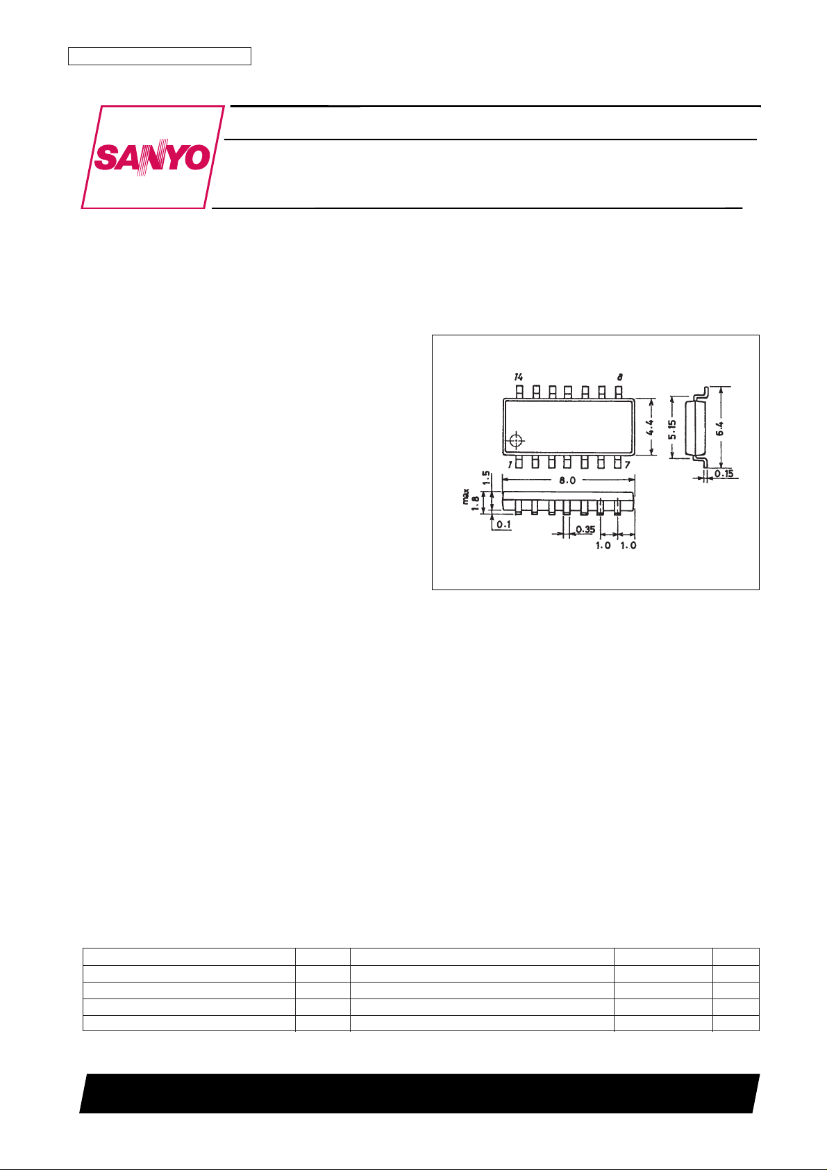
Package Dimensions
unit: mm
3111-MFP14S
CMOS LSI
Ordering number : EN5546A
73097HA (OT)/N3096HA (OT) No. 5546-1/7
SANYO: MFP14S
[LC89978M]
SANYO Electric Co.,Ltd. Semiconductor Bussiness Headquarters
TOKYO OFFICE Tokyo Bldg., 1-10, 1 Chome, Ueno, Taito-ku, TOKYO, 110 JAPAN
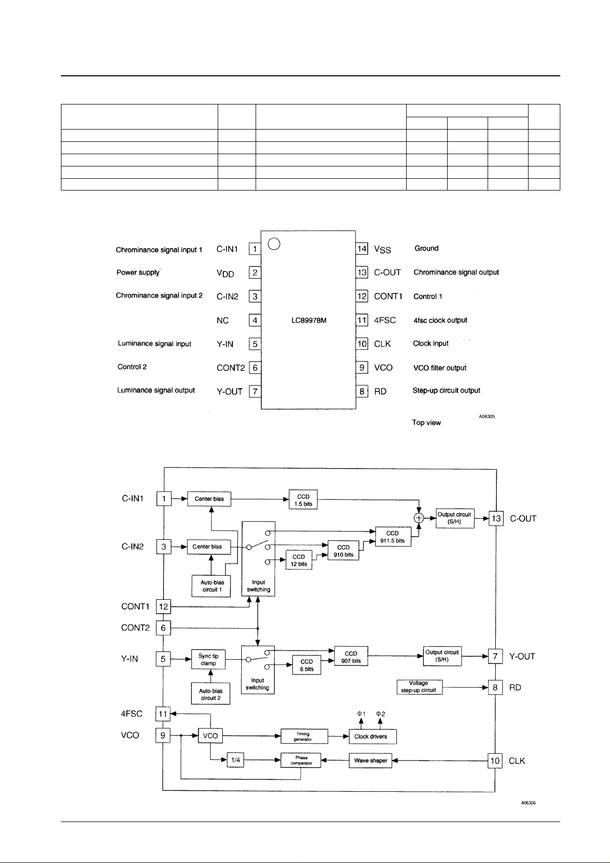
CCD Delay Line for Multi-System
LC89978M
Parameter Symbol Conditions Ratings Unit
Supply voltage V
DD
–0.3 to +6.0 V
Allowable power dissipation Pd max 250 mW
Operating temperature Topr –10 to +60 °C
Storage temperature Tstg –55 to +125 °C
Specifications
Absolute Maximum Ratings at Ta = 25°C
Page 2
No. 5546-2/7
LC89978M
Parameter Symbol Conditions
Ratings
Unit
min typ max
Supply voltage V
DD
4.75 5.00 5.25 V
Clock input amplitude V
CLK
300 500 1000 mVp-p
Clock frequency F
CLK
Sine wave 3.579545 MHz
Chrominance signal input amplitude V
IN-C
350 500 mVp-p
Luminance signal input amplitude V
IN-Y
400 572 mVp-p
Allowable Operating Ranges at Ta = 25°C
Pin Assignment
Block Diagram
Page 3
No. 5546-3/7
LC89978M
CONT1 CONT2 Mode (representative) Chrominance signal delay (number of CCD stages) Luminance signal delay (number of CCD stages)
Low Low PAL/GBI 2H (1833.5) + 0H (1.5) 1H (913)
Low High PAL/M 2H (1821.5) + 0H (1.5) 1H (907)
High Low — — —
High High NTSC/M 1H (911.5) + 0H (1.5) 1H (907)
Control Pin Functions
Parameter Symbol Conditions
Ratings
Unit
min typ max
Switching voltage level: low V
L
–0.3 0.0 +0.5 V
Switching voltage level: high V
H
2.0 5.0 6.0 V
Switching Voltage Levels
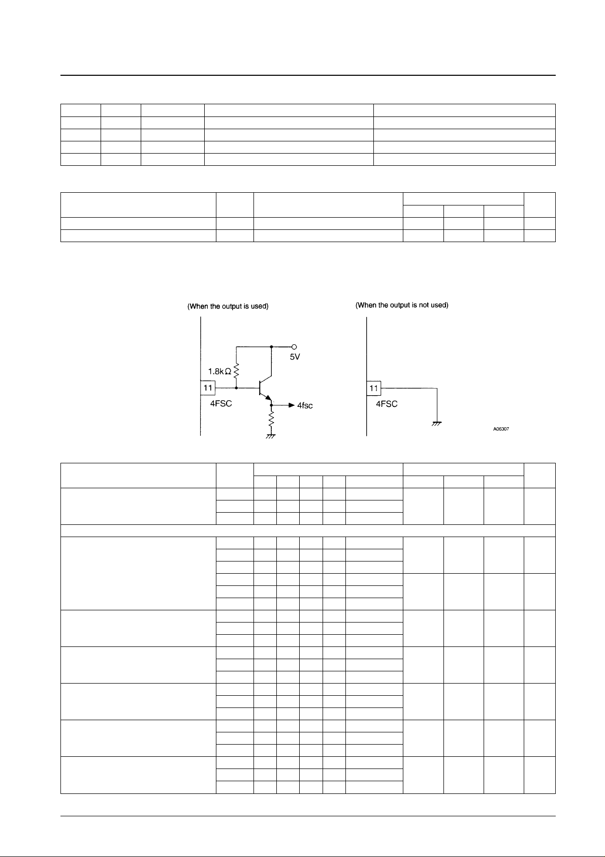
Function of the 4FSC Pin
This pin provides a 4fsc clock signal generated by the 4 × PLL frequency multiplier circuit.
Note: *Since the control pins have built-in pull-down resistors (about 70 kΩ), leaving these pins opens effectively sets them to the low level.
Continued on next page.
Parameter Symbol
Switch states Ratings
Unit
SW1 SW2 SW3 SW4 Test conditions min typ max
I
DD-1
a a a b *1
Supply current I
DD-2
a b a b *1 31 36 41 mA
I
DD-3
b b a b *1
[Chrominance signal characteristics] (with no input to Y-IN)
V
INC-1
a a a b *2
V
INC-2
a b a b *2 1.9 2.4 2.9 V
DC output voltage
V
INC-3
b b a b *2
V
OUTC-1
a a a b *2
V
OUTC-2
a b a b *2 1.4 1.9 2.4 V
V
OUTC-3
b b a b *2
G
VC-1
a a a b *3
Voltage gain G
VC-2
a b a b *3 –2 0 +2 dB
G
VC-3
b b a b *3
C
D-1
a a a b *4
Comb depth C
D-2
a b a b *4 –40 –35 dB
C
D-3
b b a b *4
L
NC-1
a a a b *5
Linearity L
NC-2
a b a b *5 –0.3 0.0 +0.3 dB
L
NC-3
b b a b *5
L
CK4C-1
a a a b *6
Clock leakage (4fsc) L
CK4C-2
a b a b *6 10 50 mVrms
L
CK4C-3
b b a b *6
L
CK1C-1
a a a b *6
Clock leakage (fsc) L
CK1C-2
a b a b *6 0.5 1.5 mVrms
L
CK1C-3
b b a b *6
Electrical Characteristics at VDD= 5.0 V, Ta = 25°C, F
CLK
= 3.579545 MHz, V
CLK
= 500 mVp-p
Page 4

No. 5546-4/7
LC89978M
Continued from preceding page.
Parameter Symbol
Switch states Ratings
Unit
SW1 SW2 SW3 SW4 Test conditions min typ max
N
C-1
a a a b *7
Noise N
C-2
a b a b *7 0.5 2.0 mVrms
N
C-3
b b a b *7
Z
OC-1
a a a a, b *8
Output impedance Z
OC-2
a b a a, b *8 200 350 500 Ω
Z
OC-3
b b a a, b *8
T
DC-1
a a a b *9
0-H delay time T
DC-2
a b a b *9 160 ns
T
DC-3
b b a b *9
[Luminance signal characteristics] (With no signals input to C-IN1 and C-IN2)
V
INY-1
a a a b *10
V
INY-2
a b a b *10 1.3 1.8 2.3 V
DC output voltage
V
INY-3
b b a b *10
V
OUTY-1
a a a b *10
V
OUTY-2
a b a b *10 0.7 1.2 1.7 V
V
OUTY-3
b b a b *10
G
VY-1
a a a b *11
Voltage gain G
VY-2
a b a b *11 –2 0 +2 dB
G
VY-3
b b a b *11
G
FY-1
a a b b *12
Frequency response G
FY-2
a b b b *12 –2 0 +2 dB
G
FY-3
b b b b *12
D
GY-1
a a a b *13
Differential gain D
GY-2
a b a b *13 0 5 8 %
D
GY-3
b b a b *13
D
PY-1
a a a b *13
Differential phase D
PY-2
a b a b *13 0 5 8 deg
D
PY-3
b b a b *13
L
SY-1
a a a b *14
Linearity L
SY-2
a b a b *14 37 40 43 %
L
SY-3
b b a b *14
L
CK4Y-1
a a a b *15
Clock leakage (4fsc) L
CK4Y-2
a b a b *15 10 50 mVrms
L
CK4Y-3
b b a b *15
L
CK1Y-1
a a a b *15
Clock leakage (fsc) L
CK1Y-2
a b a b *15 0.5 1.5 mVrms
L
CK1Y-3
b b a b *15
N
Y-1
a a a b *16
Noise N
Y-2
a b a b *16 0.5 2.0 mVrms
N
Y-3
b b a b *16
Z
OY-1
a a a c, b *17
Output impedance Z
OY-2
a b a c, b *17 250 400 550 Ω
Z
OY-3
b b a c, b *17
T
DY-1
a a a b *18 63.81 µs
Delay time T
DY-2
a b a b *18 63.39 µs
T
DY-3
b b a b *18 63.39 µs
Page 5

Test Conditions
1. The supply current with no input signal
2. The pin output voltage (the center bias voltage) with no input signal
3. Measure the C-OUT output when a 350-mVp-p sine wave is input to C-IN1 and C-IN2.
C-OUT output [mVp-p]
GVC= 20log —————————— [dB]
350 [mVp-p]
Test frequencies:
G
VC-1
: 4.431395 MHz (PAL/GBI)
G
VC-2
: 3.571628 MHz (PAL/M)
G
VC-3
: 3.571628 MHz (NTSC/M)
4. Measure the comb depth from the C-OUT output when a 350-mVp-p sine wave with frequency fa is input to C-IN1
and C-IN2, and when a sine wave of frequency fb is input.
The C-OUT output for an fb input [mVp-p]
CD= 20log —————————————————— [dB]
The C-OUT output for an fa input [mVp-p]
Test Frequencies
fa fb
C
D-1
: 4.431395 MHz (PAL/GBI) 4.435303 (PAL/GBI)
G
D-2
: 3.571628 MHz (PAL/M) 3.575561 (PAL/M)
G
D-3
: 3.571628 MHz (NTSC/M) 3.563761 (NTSC/M)
5. Measure the C-OUT output when a 200-mVp-p sine wave is input to C-IN1 and C-IN2, and when a 500-mVp-p sine
wave is input, and calculate the gain difference as follows:
The output for a 500-mVp-p input [mVp-p] The output for a 200-mVp-p input [mVp-p]
LNC= 20log —————————————————— —————————————————— [dB]
500 [mVp-p] 200 [mVp-p]
Test Frequencies
L
NC-1
4.431395MHz (PAL/GBI)
L
NC-2
3.571628MHz (PAL/M)
L
NC-3
3.571628MHz (NTSC/M)
6. Measure the 4fsc (14.3 MHz) and fsc (3.58 MHz) components in the C-OUT output with no input signal.
7. Measure the noise in the C-OUT output with no input signal.
Measure the noise with a noise meter with a 200-kHz high-pass filter and a 5-MHz low-pass filter.
8. Input a 350-mVp-p sine wave to C-IN1 and C-IN2. Let V1 be the C-OUT output when SW3 is set to the ‘a’ position,
and let V2 be the C-OUT output when SW3 is set to the 'b' position.
V2 [mVp-p] – V1 [mVp-p]
ZOC= ——————————— ×500 [dB]
V1 [mVp-p]
Test Frequencies
Z
OC-1
: 4.431395 MHz (PAL/GBI)
Z
OC-2
: 3.571628 MHz (PAL/M)
Z
OC-3
: 3.571628 MHz (NTSC/M)
9. The delay time in the C-OUT output with respect to the C-IN1 input. This is the CCD 1.5-bit delay.
10. The pin output voltage (clamp voltage) with no input signal.
No. 5546-5/7
LC89978M
( )
Page 6

11. Measure the Y-OUT output with a 200-kHz 400-mVp-p sine wave input to Y-IN.
Y-OUT output [mVp-p]
GVY= 20log —————————— [dB]
400 [mVp-p]
12. Measure the Y-OUT output when a 200-kHz 200-mVp-p sine wave is input to Y-IN, and when a 3.5-MHz
200-mVp-p sine wave is input.
The Y-OUT output for a 3.5-MHz input [mVp-p]
GFY= 20log ————————————————————— [dB]
The Y-OUT output for a 200-kHz input [mVp-p]
Here, adjust Vbias so that the clamp level is +250 mV.
13. Apply a 5-step staircase wave (as in the figure below) to Y-IN, and measure the differential gain and differential
phase in the Y-OUT output using a vector scope.
14. Apply a 5-step staircase wave (as in the figure below) to Y-IN, and measure the luminance level (Y) and the sync
level (S) in the Y-OUT output.
S [mV]
LS= ———— × 100 [%]
Y [mV]
15. Measure the 4fsc (14.3 MHz) and fsc (3.58 MHz) components in the Y-OUT output with no input signal.
16. Measure the noise in the Y-OUT output with no input signal.
Measure the noise with a noise meter with a 200-kHz low-pass filter, a 4.2-MHz low-pass filter, and a 3.58-MHz trap
filter.
17. Input a 200-kHz, 400-mVp-p sine wave to Y-IN1. Let V1 be the V-OUT output when SW3 is set to the ‘c’ position,
and let V2 be the Y-OUT output when SW3 is set to the ‘b’ position.
V2 [mVp-p] – V1 [mVp-p]
ZOY= ———————————— × 500 [Ω]
V1 [mVp-p]
18. Measure the delay time in the Y-OUT output with respect to the input to Y-IN.
No. 5546-6/7
LC89978M
Page 7

No. 5546-7/7
LC89978M
Test Circuit
This catalog provides information as of July, 1997. Specifications and information herein are subject to change
without notice.
■ No products described or contained herein are intended for use in surgical implants, life-support systems, aerospace
equipment, nuclear power control systems, vehicles, disaster/crime-prevention equipment and the like, the failure of
which may directly or indirectly cause injury, death or property loss.
■ Anyone purchasing any products described or contained herein for an above-mentioned use shall:
➀
Accept full responsibility and indemnify and defend SANYO ELECTRIC CO., LTD., its affiliates, subsidiaries and
distributors and all their officers and employees, jointly and severally, against any and all claims and litigation and all
damages, cost and expenses associated with such use:
➁
Not impose any responsibility for any fault or negligence which may be cited in any such claim or litigation on
SANYO ELECTRIC CO., LTD., its affiliates, subsidiaries and distributors or any of their officers and employees
jointly or severally.
■ Information (including circuit diagrams and circuit parameters) herein is for example only; it is not guaranteed for
volume production. SANYO believes information herein is accurate and reliable, but no guarantees are made or implied
regarding its use or any infringements of intellectual property rights or other rights of third parties.
 Loading...