

Page 1
CMOS LSI
Ordering number : EN*5420
93096HA (OT) No. 5420-1/6
SANYO Electric Co.,Ltd. Semiconductor Bussiness Headquarters
TOKYO OFFICE Tokyo Bldg., 1-10, 1 Chome, Ueno, Taito-ku, TOKYO, 110 JAPAN
NTSC Format Delay Line
LC89962, LC89962M
Overview
The LC89962 and LC89962M are delay line circuits that
provide a delayed signal by a 1H period of NTSC format
with an external low-pass filter.
Features
• Requires only the input of a 3.58-MHz clock to produce
a 1H delayed signal and the external low-pass filter.
• Uses a 5-V single-voltage power supply.
• Requires a minimal number of external components due
to the peripheral components provided on chip.
• Output signal has the same phase as the input signal.
• Operation has a 4fsc clock synchronized with the input
clock allows these products to be used as wide
bandwidth delay lines.
• A 4fsc clock can be output from the 4FSC pin (pin 7).
Functions
• 906-bit CCD shift register
• Timing generator and CCD driver circuits
• Auto-bias circuit
• Sync-tip clamp circuit
• Sample-and-hold and output amplifier circuits
•4 × PLL circuit
• 4fsc output circuit
Specifications
Absolute Maximum Ratings at Ta = 25°C
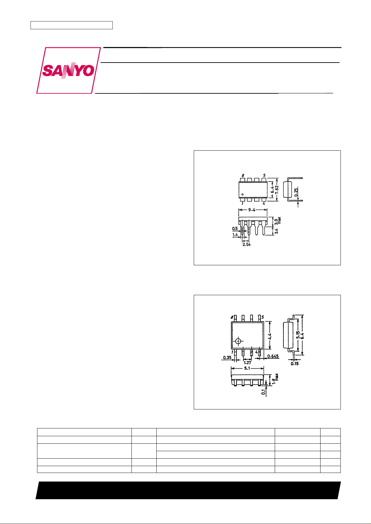
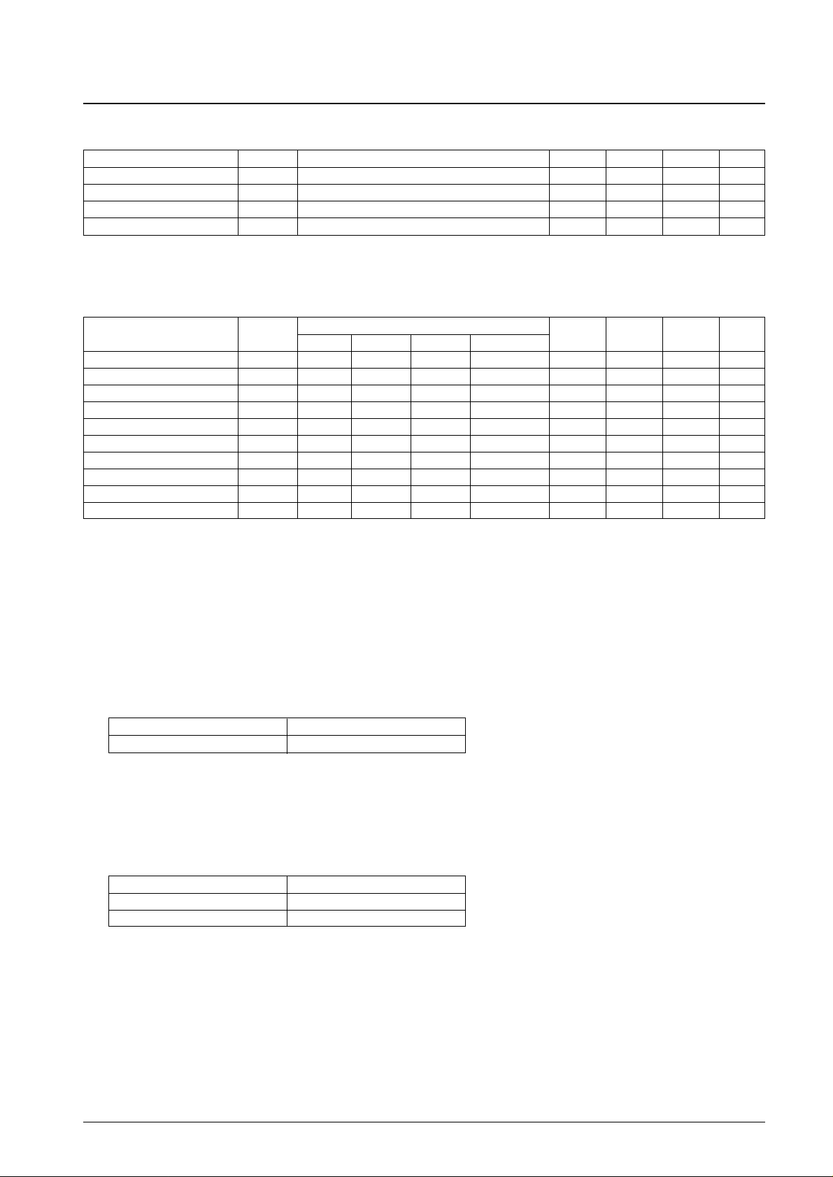
Package Dimensions
unit: mm
3001B-DIP8
unit: mm
3032B-MFP8
SANYO: DIP8
[LC89962]
SANYO: MFP8
[LC89962M]
Parameter Symbol Conditions Ratings Unit
Supply voltage V
DD
–0.3 to +6.0 V
Allowable power dissipation Pd max
LC89962 400 mW
LC89962M 140 mW
Operating temperature Topr –10 to +60 °C
Storage temperature Tstg –55 to +125 °C
Page 2
Allowable Operating Ranges at Ta = 25°C
Note 1. The input signal must be input with low impedance for correct operation of sync-tip clamping.
Electrical Characteristics at Ta = 25°C, VDD= 5.0 V, CLK = 3.579545 MHz; 300 mV p-p
Test Conditions
1. The supply current with no input signal
2. The following formula is used to calculate the voltage gain (GV).
V
OUT
[mVp-p]
GV= 20log ——————— [dB]
500 [mVp-p]
3. The following formula is used to calculate the frequency characteristics (Gf).
V2 [mVp-p]
Gf= 20log —————— [dB]
V1 [mVp-p]
During this test, adjust Vbias so that the input signal DC level is 250 mV higher than the clamp level.
No. 5420-2/6
LC89962, LC89962M
Parameter Symbol
Switch states
min typ max Unit
SW1 SW2 SW3 Test conditions
Supply current I
DD
a a a *1 5 15 25 mA
Voltage gain G
V
a b a *2 –2 0 +2 dB
Frequency characteristics G
f
b b a *3 –2 –1 0 dB
Differential gain DG a a a *4 0 5 %
Differential phase DP a a a *4 0 5 deg
Linearity LS a a a *5 37 40 43 %
Clock leakage Lck a b a *6 5 50 mVrms
Noise N
O
a b a *7 1 2 mVrms
Output impedance Z
O
a b a↔b *8 220 370 520 Ω
Delay time TD a b a *9 63.33 µs
Parameter Symbol Conditions min typ max Unit
Supply voltage V
DD
4.75 5.0 5.25 V
Clock input amplitude V
CLK
Sine wave 200 300 500 mVp–p
Clock frequency F
CLK
3.579545 MHz
Signal input amplitude V
IN
(*1) 500 572 mVp–p
Output signal symbol Input signal
V
OUT
Sine wave: 200 kHz, 500 mV p-p
Output signal symbol Input signal
V1 Sine wave: 200 kHz, 200 mV p-p
V2 Sine wave: 3.58 MHz, 200 mV p-p
Page 3

4. Measure the differential gain (DG) and differential phase (DP) using a vector scope with a 5-step function wave
input. (See the following figure.)
5. To measure LS, input a 5-step function wave and measure the ratio of the sync level (S) to the luminance level (Y).
S [mV]
LS = ———— × 100 [%]
Y [mV]
6. To measure clock leakage (Lck), measure the 4fsc (14.3 MHz) component in the output signal with a spectrum
analyzer when no input signal is presented.
7. To measure the noise level (NO), measure the noise output in the OUT pin output when no input signal is present
with a video noise meter. Set up the noise meter with a 200-kHz high-pass filter, a 4.2-MHz low-pass filter, and
3.58-MHz trap filter.
8. The following formula is used to calculate the output impedance (ZO).
V1 [mVp-p] – V2 [mVp-p]
ZO= ——————————— × 500 [Ω]
V2 [mVp-p]
9. To measure the delay time (TD), measure the delay time of the output signal to the input signal. In this measurement,
the delay time associated with the low-pass filter must be excluded.
No. 5420-3/6
LC89962, LC89962M
Output signal symbol SW3 Input signal
V1 a
Sine wave: 200 kHz, 500 mV p-p
V2 b
Page 4

Pin Assignment
Block Diagram
No. 5420-4/6
LC89962, LC89962M
Page 5

Test Circuit
Sample Application Circuit
No. 5420-5/6
LC89962, LC89962M
Page 6

4FSC (pin 7) Sample Application Circuit
No. 5420-6/6
LC89962, LC89962M
This catalog provides information as of September, 1996. Specifications and information herein are subject to
change without notice.
■ No products described or contained herein are intended for use in surgical implants, life-support systems, aerospace
equipment, nuclear power control systems, vehicles, disaster/crime-prevention equipment and the like, the failure of
which may directly or indirectly cause injury, death or property loss.
■ Anyone purchasing any products described or contained herein for an above-mentioned use shall:
➀ Accept full responsibility and indemnify and defend SANYO ELECTRIC CO., LTD., its affiliates, subsidiaries and
distributors and all their officers and employees, jointly and severally, against any and all claims and litigation and all
damages, cost and expenses associated with such use:
➁ Not impose any responsibility for any fault or negligence which may be cited in any such claim or litigation on
SANYO ELECTRIC CO., LTD., its affiliates, subsidiaries and distributors or any of their officers and employees
jointly or severally.
■ Information (including circuit diagrams and circuit parameters) herein is for example only; it is not guaranteed for
volume production. SANYO believes information herein is accurate and reliable, but no guarantees are made or implied
regarding its use or any infringements of intellectual property rights or other rights of third parties.
 Loading...