

Page 1
Overview
The LC89901V is a high breakdown voltage CMOS
vertical driver IC for 1/5 and 1/6 inch image sensors.
Provision of a built-in level shifter means that an external
clamp circuit is no longer required.
Applications
Surveillance cameras and image input equipment
Functions
CMOS driver IC for 1/5 and 1/6 inch image sensors
Features
• CMOS process fabrication for low power dissipation
• Built-in level shifter circuits to reduce the number of
required peripheral circuits.
• Miniature package (SSOP-24)
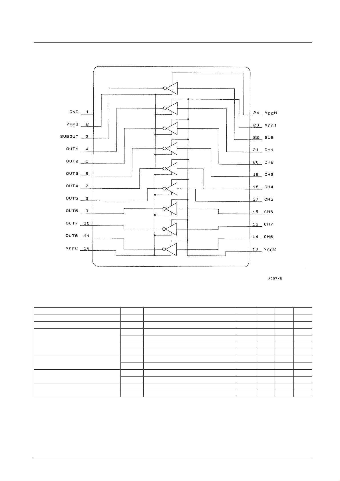
Structure
• Inverter type drivers: 8 channels
Input pulses are converted to VCC1, VCC2 and VEE1,
VEE2 levels (inversion).
These are drivers for image sensor imaging and storage
sections.
• Inverter type driver: 1 channel
Input pulses are converted to VCCN and VEE1, VEE2
levels (inversion).
This circuit is an image sensor NSUB driver.
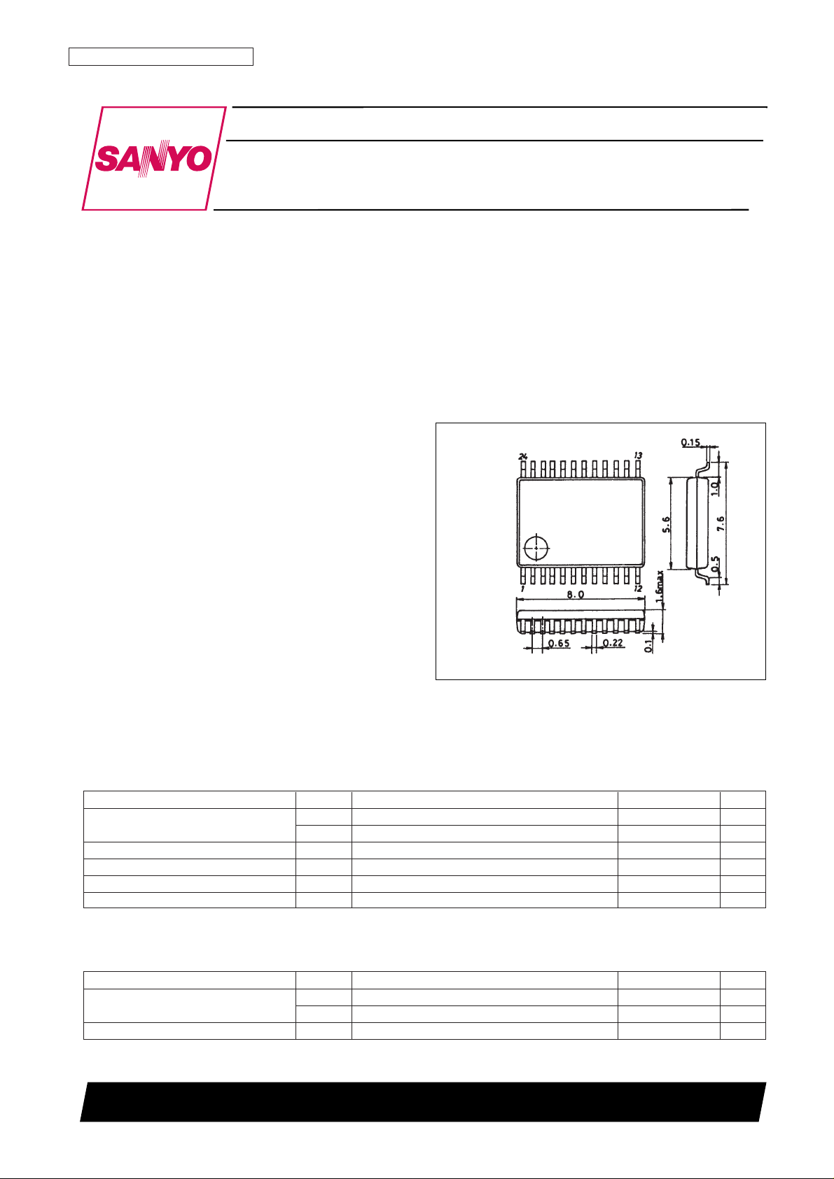
Package Dimensions
unit: mm
3175A-SSOP24
CMOS LSI
Ordering number : EN5078A
73097HA (OT)/32895TH (OT) NO. 5078-1/4
SANYO: SSOP24
[LC89901V]
SANYO Electric Co.,Ltd. Semiconductor Bussiness Headquarters
TOKYO OFFICE Tokyo Bldg., 1-10, 1 Chome, Ueno, Taito-ku, TOKYO, 110 JAPAN
CMOS Driver IC for 1/5 and 1/6 Inch
Image Sensors
LC89901V
Specifications
Absolute Maximum Ratings at Ta = 25°C
Allowable Operating Ranges at Ta = 25°C
Parameter Symbol Conditions Ratings Unit
Maximum supply voltage
V
CC
max VCC1, VCC2, VCCN –0.3 to +6.0 V
V
EE
max VEE1, VEE2 +0.3 to –11.0 V
Input voltage V
IN
All input pins –0.3 to VCC+ 0.3 V
Allowable power dissipation Pd max 350 mA
Operating temperature Topr –10 to +70 °C
Storage temperature Tstg –40 to +125 °C
Parameter Symbol Conditions Ratings Unit
Supply voltage
V
CC
VCC1, VCC2, VCCN : *VCCN ≤ VCC1, VCC2 4.5 to 5.5 V
V
EE
VEE1, VEE2 0 to –10.5 V
Input voltage range V
IN
All input pins 0 to V
CC
V
Page 2
Block Diagram
Electrical Characteristics at Ta = 25°C, VCC1, VCC2, VCCN = 5.0 V, VEE1, VEE2 = –10.0 V
Note: Load conditions
Load circuit
* Reference values for driving an LC9997 image sensor with pulses input from an LC99052 timing LSI.
NO. 5078-2/4
LC89901V
Parameter Symbol Conditions min typ max Unit
Input high level current I
IH
All input pins, VIN= 5.0 V 10 µA
Input low level current I
IL
All input pins, VIN= 0 V 5 nA
I
CCH
+ V
CC
1, VCC2, VCCN, all input pins, VIN= 5.0 V 1 µA
Current drain
I
CCH
– V
EE
1, VEE2, all input pins, VIN= 5.0 V –10 µA
I
CCL
+ V
CC
1, VCC2, VCCN, all input pins, VIN= 0 V 7 µA
I
CCH
– V
EE
1, VEE2, all input pins, VIN= 0 V –2 µA
Output voltage
V
OH
All inputs, VIN= 0 V 5.0 V
V
OL
All inputs, VIN= 5.0 V –10.0 V
Operating output voltage*
V
OH
2 Load = LC9997, input = LC99052 5.0 V
V
OL
2 Load = LC9997, input = LC99052 –10.0 V
Operating current drain*
I
CC
2+Load = LC9997, input = LC99052 1.62 mA
I
CC
2–Load = LC9997, input = LC99052 1.61 mA
RL= 18 Ω, CL= 780 pF
Page 3

Switching Characteristics at Ta = 25°C, VCC1, VCC2, VCCN = 5.0 V, VEE1, VEE2 = –10.0 V, fIN= 3.58 MHz
Switching Waveforms
Truth table
NO. 5078-3/4
LC89901V
Parameter Symbol Conditions min typ max Unit
Propagation delay
t
PLH
All output pins 23 ns
Low level → high level tpLH
Propagation delay
t
PHL
All output pins 31 ns
High level → low level tpHL
Rise time t
r
All output pins 47 ns
Fall time t
f
All output pins 42 ns
Pin Functions
Output
Input
H V
OL
L V
OH
Pin No. Pin Function
1 GND Ground
2 V
EE
1 Negative power supply for setting the low level
3 SUBOUT NSUB driver output
4 OUT1 Channel 1 driver output
5 OUT2 Channel 2 driver output
6 OUT3 Channel 3 driver output
7 OUT4 Channel 4 driver output
8 OUT5 Channel 5 driver output
9 OUT6 Channel 6 driver output
10 OUT7 Channel 7 driver output
11 OUT8 Channel 8 driver output
12 V
EE
2 Negative power supply for setting the low level
13 V
CC
2 Positive power supply for setting the high level
14 CH8 Channel 8 driver input
15 CH7 Channel 7 driver input
16 CH6 Channel 6 driver input
17 CH5 Channel 5 driver input
18 CH4 Channel 4 driver input
19 CH3 Channel 3 driver input
20 CH2 Channel 2 driver input
21 CH1 Channel 1 driver input
22 SUB NSUB driver input
23 V
CC
1 Positive power supply for setting the high level
24 V
CC
N NSUB driver positive power supply
Page 4

Sample Application Circuit
This figure shows the block diagram of an image sensor based digital camera using the Sanyo LC99052–V64,
LC99062–W50 and LC89901V.
NO. 5078-4/4
LC89901V
This catalog provide information as of June, 1997. Specifications and information herein are subject to change
without notice.
■ No products described or contained herein are intended for use in surgical implants, life-support systems, aerospace
equipment, nuclear power control systems, vehicles, disaster/crime-prevention equipment and the like, the failure of
which may directly or indirectly cause injury, death or property loss.
■ Anyone purchasing any products described or contained herein for an above-mentioned use shall:
➀ Accept full responsibility and indemnify and defend SANYO ELECTRIC CO., LTD., its affiliates, subsidiaries and
distributors and all their officers and employees, jointly and severally, against any and all claims and litigation and all
damages, cost and expenses associated with such use:
② Not impose any responsibility for any fault or negligence which may be cited in any such claim or litigation on
SANYO ELECTRIC CO., LTD., its affiliates, subsidiaries and distributors or any of their officers and employees
jointly or severally.
■ Information (including circuit diagrams and circuit parameters) herein is for example only; it is not guaranteed for
volume production. SANYO believes information herein is accurate and reliable, but no guarantees are made or implied
regarding its use or any infringements of intellectual property rights or other rights of third parties.
 Loading...