

Page 1
CMOS LSI
Ordering number : *EN5572
22897HA (OT) No. 5572-1/11
Preliminary
LC897194
SANYO Electric Co.,Ltd. Semiconductor Bussiness Headquarters
TOKYO OFFICE Tokyo Bldg., 1-10, 1 Chome, Ueno, Taito-ku, TOKYO, 110 JAPAN
CD-ROM Decoder with Built-In ATAPI (IDE) and DVD
ECC Interfaces
Overview
The LC897194 provides CD-ROM functionality and
includes built-in DVD ECC and ATAPI (IDE) interfaces.
Function
• CD-ROM ECC functionality, an ATAPI (IDE) interface
(the register and other blocks), and a DVD ECC
interface
Features
• ATAPI (IDE) interface
• DVD ECC interface
• Supports up to 12×-speed playback (when using 70-ns
16-bit data path DRAM)
• Transfer rate: 16.6 MB/s (when using 60-ns 16-bit data
path DRAM)
• Transfer rate: 8.33 MB/s (when using 70-ns 8-bit data
path DRAM)
• Between 1 and 32 Mbits of DRAM can be used as buffer
RAM.
• The user can freely set up the CD main channel and the
C2 flags in buffer RAM.
• Built-in batch transfer function (function for transferring
the CD main channel and the C2 flags in one operation)
• Built-in multiple transfer function (function for
automatically transferring multiple blocks in a single
operation)
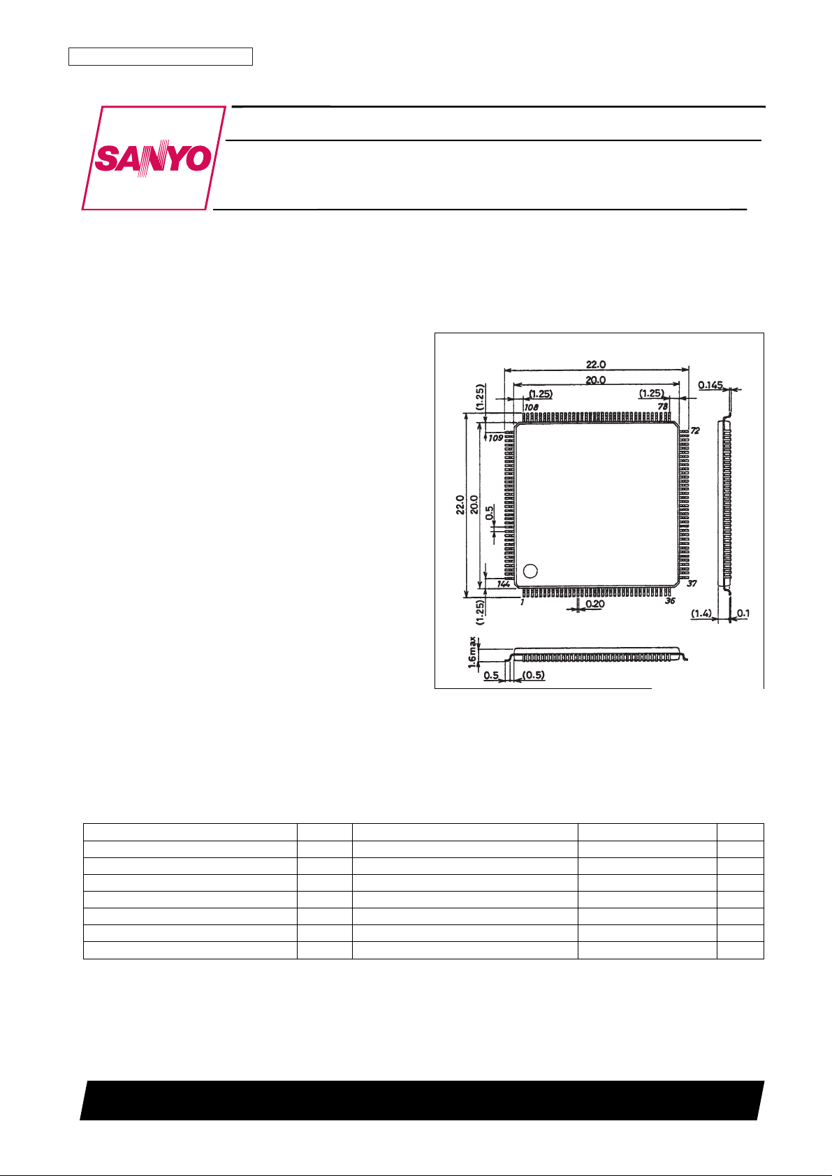
Package Dimensions
unit: mm
3214-SQFP144
SANYO: SQFP144
[LC897194]
Parameter Symbol Conditions Ratings Unit
Maximum supply voltage V
DD
max Ta = 25°C –0.3 to +7.0 V
I/O voltages V
I
, VOTa = 25°C –0.3 to VDD+0.3 V
Allowable power dissipation Pd max Ta ≤ 70°C 550 mW
Operating temperature Topr –30 to +70 °C
Storage temperature Tstg –55 to +125 °C
Soldering heat resistance (pins only) 10 seconds 235 °C
Maximum I/O power I
I
, IOmax ±20* mA
Specifications
Absolute Maximum Ratings at VSS= 0 V
Note: Per basic I/O cell.
Page 2
No. 5572-2/11
LC897194
Parameter Symbol Applicable pins (see below)
Ratings
Unit
min typ max
Input high-level voltage V
IH1
TTL compatible: (1) 2.2 V
Input low-level voltage V
IL1
TTL compatible: (1) 0.8 V
Input high-level voltage V
IH2
TTL compatible, with pull-up resistor: (12) 2.2 V
Input low-level voltage V
IL2
TTL compatible, with pull-up resistor: (12) 0.8 V
Input high-level voltage V
IH3
TTL compatible, with pull-down resistor: (2) 2.2 V
Input low-level voltage V
IL3
TTL compatible, with pull-down resistor: (2) 0.8 V
Input high-level voltage V
IH4
TTL compatible, Schmitt characteristics: (3),
2.5 V
(5), (13), (14)
Input low-level voltage V
IL4
TTL compatible, Schmitt characteristics: (3),
0.6 V
(5), (13), (14)
Input high-level voltage V
IH5
CMOS compatible, Schmitt characteristics: (4) 0.8 V
DD
V
Input low-level voltage V
IL5
CMOS compatible, Schmitt characteristics: (4) 0.2 V
DD
V
Output high-level voltage V
OH1IOH
= –2 mA : (7), (10), (12) VDD– 2.1 V
Output low-level voltage V
OL1IOL
= 2 mA : (7), (10), (12) 0.4 V
Output high-level voltage V
OH2IOH
= –8 mA : (6) VDD– 2.1 V
Output low-level voltage V
OL2IOL
= 8 mA : (6) 0.4 V
Output high-level voltage V
OH3IOH
= –4 mA : (8), (13) VDD– 2.1 V
Output low-level voltage V
OL3IOL
= 24 mA : (8), (13) 0.4 V
Output high-level voltage V
OH4IOL
= 24 mA : (9), (14) 0.4 V
Output low-level voltage V
OL5IOL
= 2 mA : (11) 0.4 V
Input leakage current I
IL
VI= VSS, VDD: (1), (2), (3), (4), (5), (12), (13),
–10 +10 µA
(14)
Output leakage current I
OZ
When the output is high impedance: (9), (11),
–10 +10 µA
(13), (14)
Pull-up resistance R
UP
(12) 40 80 160 kΩ
Pull-down resistance R
DN
(2) 40 80 160 kΩ
DC Characteristics at Ta = –30 to +70°C, VSS= 0 V, VDD= 4.5 to 5.5 V
Note: The applicable pins are as follows:
INPUT
(1) CSCTRL, RSSEL, HDB0 to 7, SUA0 to 6
(2) TEST0 to 4
(3) ZDMACK, ZHRST, ZRESET, BCK, C2PO, LRCK, SDATA, DA0 to 2, ZCS1FX, ZCS3FX
(4) ZCS, ZRD, ZWR
(5) ZDIOR, ZDIOW, DRESP, WFCK, SCOR
OUTPUT
(6) MCK, MCK2
(7) ZINT0, ZINT1
(8) DMARQ, HINTRQ
(9) IORDY, ZIOCS16
(10) RA0 to 9, ZCAS0 to 1, ZRAS0 to 1, ZLWE, ZUWE, ZOE, DREQ
(11) ZRSTCPU, ZRSTIC, ZSWAIT
INOUT
(12) D0 to 7, IO0 to 15
(13) DD0 to 15
(14) ZDASP, ZPDIAG
*: The DC characteristics do not apply to the XTAL and XTALCK pins.
Parameter Symbol Conditions
Ratings
Unit
min typ max
Supply voltage V
DD
4.5 5.0 5.5 V
Input voltage range V
IN
0 V
DD
V
Allowable Operating Ranges at Ta = –30 to +70°C, VSS= 0 V
Page 3

Recommended Oscillator Circuit Example
R1 = 120 kΩ
R2 = 47 Ω
C1 = 30 pF
With a crystal with a resonant frequency of 16.9344 MHz, or:
R1 = 3.3 kΩ
R2 = None
C1 = 5 pF
With a crystal with a resonant frequency of 33.8688 MHz.
If third harmonics are a problem in the 33.8688-MHz recommended circuit, consult with the manufacturer of the crystal
for exact component values, since those values will be influenced by the printed circuit board used.
No. 5572-3/11
LC897194
Page 4

Block Diagram
*1 BCK, SDATA, LRCK, C2PO
*2 DD0 to DD15, ZDASP, ZPDIAG
*3 ZCS1FX, ZCS3FX, DA0 to DA2, ZDIOR, ZDIOW, ZDMACK
*4 DMARQ, HINTRQ, ZIOCS16, IORDY, ZHRST
*5 ZRD, ZWR, SUA0 to SUA6, ZCS, CSCTRL
*6 D0 to D7
*7 IO0 to IO15
*8 RA0 to RA9, ZRAS0, ZRAS1, ZCAS0, ZCAS1, ZOE, ZUWE, ZLWE
*9 DREQ
*10 HDB0 to HDB7, DRESP
*11 WFCK, SCOR
**1 HISIDE (WD25C32) is made by WESTERN DIGITAL.
No. 5572-4/11
LC897194
Page 5

No. 5572-5/11
LC897194
Pin Functions
typ
I Input B Bidirection NC Not connected
O Output P Power
Pin No. Symbol Type Function
1 V
SS0
P
2 ZRAS0 O RAS signal output 0 to the buffer DRAM (Output 0 is normally used.)
3 ZRAS1 O RAS signal output 1 to the buffer DRAM
4 V
SS0
P
5 ZCAS0 O CAS signal output 0 to the buffer DRAM (Output 0 is normally used.)
6 ZCAS1 O CAS signal output 1 to the buffer DRAM
7 V
SS0
P
8 ZOE O Buffer RAM output enable
9 ZUWE O Buffer RAM upper write enable
10 ZLWE O Buffer RAM lower write enable
11 RA0 O RA0 to RA9 are used for the data buffer DRAM address.
12 RA1 O
13 RA2 O
14 RA3 O
15 RA4 O
16 RA5 O
17 RA6 O
18 V
DD
P
19 V
SS0
P
20 RA7 O RA0 to RA9 are used for the data buffer DRAM address.
21 RA8 O
22 RA9 O
23 TEST0 NC Used for testing. There should be no connections to these pins.
24 TEST1 NC These pins must be left open.
25 TEST2 NC
26 TEST3 NC
27 TEST4 NC
28 IO0 B Data I/O to/from data buffer DRAM
29 IO1 B Pull-up resistors are built in.
30 IO2 B
31 IO3 B
32 IO4 B
33 IO5 B
34 IO6 B
35 IO7 B
36 V
SS0
P
37 V
DD
P
Continued on next page.
Page 6

No. 5572-6/11
LC897194
Pin No. Symbol Type Function
38 IO8 B Data I/O to/from data buffer DRAM
39 IO9 B Pull-up resistors are built in.
40 IO10 B
41 IO11 B
42 IO12 B
43 IO13 B
44 IO14 B
45 IO15 B
46 V
SS0
P
47 WFCK I Subcode input
48 SCOR I Subcode input
49 V
SS0
P
50 DREQ O DVD ECC data request output
51 DRESP I DVD ECC data latch signal input
52 HDB7 I DVD ECC data input
53 HDB6 I
54 V
DD
P
55 V
SS0
P
56 HDB5 I DVD ECC data input
57 HDB4 I
58 HDB3 I
59 HDB2 I
60 HDB1 I
61 HDB0 I
62 SDATA I Interface with the CD digital signal processor
63 BCK I
64 LRCK I
65 C2PO I
66 MCK2 O Outputs the XTALCK signal times 1/1, 1/2, or 1/512, or stopped.
67 CSCTRL I Microcontroller chip select signal active high or low selection
68 RSSEL I Direct or indirect addressing selection
69 V
SS0
P
70 XTALCK I Crystal oscillator circuit input
71 XTAL O Crystal oscillator circuit output
72 V
SS0
P
73 V
DD
P
74 MCK O Outputs the XTALCK signal times 1/1 or 1/2, or stopped.
75 V
SS0
P
76 ZRSTIC O Reset output to the driver reset IC
77 ZRESET I LSI reset input
78 ZRD I Microcontroller data read signal input
79 ZWR I Microcontroller data write signal input
80 ZCS I Register chip select signal input from the microcontroller
81 ZINT1 O ATAPI block interrupt output (selected by a register)
82 ZINT0 O Interrupt request signal output to the microcontroller
Continued on next page.
Continued from preceding page.
Page 7

No. 5572-7/11
LC897194
Pin No. Symbol Type Function
83 SUA0 I Microcontroller register selection signals
84 SUA1 I The SUA0 pin functions as RS in indirect address mode.
85 SUA2 I
86 SUA3 I
87 SUA4 I
88 SUA5 I
89 SUA6 I
90 V
DD
P
91 V
SS0
P
92 D0 B Microcontroller data signals
93 D1 B Pull-up resistors are built in.
94 D2 B
95 D3 B
96 D4 B
97 D5 B
98 D6 B
99 D7 B
100 V
SS0
P
101 ZRSTCPU O Reset signal output to the CPU
102 ZSWAIT O WAIT signal output to the microcontroller
103 ZHRST I ATAPI control signals
104 ZDASP B
105 ZCS3FX I
106 ZCS1FX I
107 DA2 I
108 V
SS0
P
109 V
DD
P
110 DA0 I ATAPI control signals
111 ZPDIAG B
112 DA1 I
113 ZIOCS16 O
114 HINTRQ O
115 ZDMACK I
116 V
SS1
P
117 IORDY O ATAPI control signals
118 ZDIOR I
119 ZDIOW I
120 DMARQ O
121 DD15 B ATAPI data bus
122 V
SS1
P
123 DD0 B ATAPI data bus
124 DD14 B
125 DD1 B
Continued on next page.
Continued from preceding page.
Page 8

No. 5572-8/11
LC897194
Pin No. Symbol Type Function
126 V
DD
P
127 V
SS1
P
128 DD13 B ATAPI data bus
129 DD2 B
130 DD12 B
131 DD3 B
132 V
SS1
P
133 DD11 B ATAPI data bus
134 DD4 B
135 DD10 B
136 V
SS1
P
137 V
DD
P
138 DD5 B ATAPI data bus
139 DD9 B
140 DD6 B
141 V
SS1
P
142 DD8 B ATAPI data bus
143 DD7 B
144 V
DD
P
Continued from preceding page.
NC pins must be left open. Make no connections to these pins.
Pin symbols that start with the letter Z are negative logic signals.
V
SS0
is the logic system ground and V
SS1
is the IDE interface driver ground.
Page 9

Pin Descriptions
1. ATAPI Pins
ZCS1FX (input)
Chip select signal used to select the command block register.
ZCS3FX (input)
Chip select signal used to select the control block register.
DA0 to DA2 (input)
Address used to access the ATAPI registers.
ZDASP(input/output)
Drive 1 is output, drive 0 is input.
Signal used to indicate to drive 0 that drive 1 exists. An external pull-up resistor must be provided.
DD0 to DD15 (input/output)
Data bus with a width of 16 bits. Data can be transferred in 8-bit and 16-bit units.
ZDIOR (input)
Read strobe signal from the host.
ZDIOW (input)
Write strobe signal from the host.
ZDMACK (input)
Acknowledge signal from the host in response to a drive DMARQ request signal during DMA transfers.
There is no internal pull-up resistor in the pin circuit.
DMARQ (output)
Drive request signal during DMA transfers.
HINTRQ (output)
Drive interrupt signal sent to the host.
ZIOCS16 (output)
This signal is asserted by the drive when the drive can support 16-bit transfers.
This signal is not asserted during DMA transfers.
IORDY (output)
Signal that indicates that the drive has completed response preparation during data transfers.
This signal will be low when preparation has not completed.
ZPDIAG (input/output)
Signal asserted by drive 1 to inform drive 0 that the diagnostics have completed. An external pull-up resistor
must be provided.
ZHRST (input)
Reset signal from the host.
There is no internal pull-up resistor in the pin circuit.
2. Microcontroller Interface Pins
ZCS (input)
Chip select signal from the microcontroller.
CSCTRL (input)
Signal that selects the logic of the chip select from the microcontroller.
High - The ZCS signal functions as an active-low signal.
Low - The ZCS signal functions as an active-high signal.
ZRD, ZWR, SUA0 to SUA6 (input)
Microcontroller interface control pins. The SUA0 to SUA6 pins are used for addressing.
SUA0 functions as RS (the register select pin) in indirect addressing.
When SUA0 is low, and address read or write operation is performed, and when high, a data read or write
operation is performed.
RSSEL (input)
Signal that selects direct or indirect addressing.
High - Indirect addressing selected.
Low - Direct addressing selected.
ZSWAIT (output)
When the microcontroller is accessing RAM, the sub-CPU must wait when this pin is low.
D7 to D0 (input/output)
Microcontroller data bus. Pull-up resistors are built in.
ZINT0 (output)
Interrupt request signal to the microcontroller.
The active level (high or low) can be changed by setting a register. The default setting is active low.
ZINT1 (output)
Interrupt request signal from the IDE block to the microcontroller.
No. 5572-9/11
LC897194
Page 10

No. 5572-10/11
LC897194
3. Buffer RAM Pins
IO0 to IO15 (input/output)
Data bus for the buffer DRAM. Pull-up resistors are built in.
RA0 to RA9 (output)
Buffer RAM address pins.
ZRAS0, ZRAS1 (ZCS0, ZCS1) (output)
Buffer DRAM RAS output pins. Although ZRAS0 is used normally, in applications that use two 1M (64K × 16
bits) DRAMs, the ZRAS0 and ZRAS1 signals can be connected to each of DRAM RAS pins.
ZCAS0, ZCAS1 (output)
Buffer DRAM CAS output pins. Although ZCAS0 is used normally, in applications that use two-CAS DRAMs,
the ZCAS0 can be connected to the DRAM UCAS pin, and ZCAS1 to the DRAM LCAS pin.
ZOE (output)
The buffer DRAM read output pin.
ZUWE, ZLWE (output)
Buffer DRAM write output signals. Connect these pins to the corresponding pins on the DRAMs.
When two-CAS DRAMs are used, connect ZLWE to the write enable signal.
4. Subcode Interface Pins
WFCK, SCOR (input)
Subcode interface pins. By connecting these pins to the CD DSP, the subcode sync can be detected and the CD
main channel buffering can be started according to that sync. Subcode data buffering and ECC are not
performed.
5. CD DSP Data Pins
BCK, SDATA, LRCK, C2PO (input)
Connect these pins to the CD DSP to acquire the CD-ROM data.
C2PO is the C2 flag pin.
6. DVD ECC interface pins
DRESP (input)
DVD ECC data is latched on the falling edge of this signal.
HDB0 to HDB7 (input)
DVD ECC data input pins.
DREQ (output)
DVD ECC data request output.
7. Other Pins
ZRESET (input)
The LC897194 reset pin. The LSI is reset when a low level is applied.
Applications must hold this pin low for at least 1 µs when power is first applied.
XTALCK, XTAL
These pins drive an external crystal at either 16.9344 MHz or 33.8688 MHz.
An external clock frequency can also be input to the XTALCK pin.
MCK (output)
Outputs either the XTALCK frequency or that frequency divided by 2. This output can be stopped.
MCK2 (output)
Outputs either the XTALCK frequency or that frequency divided by 2 (with the opposite phase of the MCK pin)
or the XTALCK frequency divided by 512. This output can be stopped.
ZRSTIC (output)
This pin can be set to output a low level by either setting bit 7 in the microcontroller register R46 (ZSYSRES)
low (0), or setting the ZHRST pin (pin 103) low. This pin output is in the high-impedance state when both
ZSYSRES and ZHRST are high.
Since this pin has an open-drain circuit, an external pull-up resistor must be provided.
ZRSTCPU (output)
A low-going pulse of about 1 ms (when XTALCK = 34 MHz, or about 2 ms when XTALCK = 16 MHz) is
generated on this pin when an ATAPI soft reset command (08H) is received.
An interrupt is issued to the microcontroller at this time. If the ZRESET pin (pin 77) is functioning with activelow logic, the ZRESET signal is output without change to ZRSTCPU.
Since this pin has an open-drain circuit, an external pull-up resistor must be provided.
Page 11

No. 5572-11/11
LC897194
This catalog provides information as of February, 1997. Specifications and information herein are subject to
change without notice.
■ No products described or contained herein are intended for use in surgical implants, life-support systems, aerospace
equipment, nuclear power control systems, vehicles, disaster/crime-prevention equipment and the like, the failure of
which may directly or indirectly cause injury, death or property loss.
■ Anyone purchasing any products described or contained herein for an above-mentioned use shall:
➀
Accept full responsibility and indemnify and defend SANYO ELECTRIC CO., LTD., its affiliates, subsidiaries and
distributors and all their officers and employees, jointly and severally, against any and all claims and litigation and all
damages, cost and expenses associated with such use:
➁
Not impose any responsibility for any fault or negligence which may be cited in any such claim or litigation on
SANYO ELECTRIC CO., LTD., its affiliates, subsidiaries and distributors or any of their officers and employees
jointly or severally.
■ Information (including circuit diagrams and circuit parameters) herein is for example only; it is not guaranteed for
volume production. SANYO believes information herein is accurate and reliable, but no guarantees are made or implied
regarding its use or any infringements of intellectual property rights or other rights of third parties.
 Loading...