

Page 1
Overview
The LC895925 provides the following signal processing
functions for CD-R drives: CD-ROM decoding/encoding
(complete with ECC processing for the former), subcode
decoding/encoding, CD encoding, ATIP decoding, CLV
servo, and SCSI interface registers.
Features
• CD-ROM decoding/encoding complete with error
detection and error correction
• Subcode decoding/encoding complete with error
correction
• ATIP decoding and CRC checking for both encoding
and decoding
• CLV servo control using ATIP data during encoding
• CIRC code insertion and EFM modulation during
encoding
• Support for PCA random EFM output during encoding
• Support for CD-ReWritable (CD-RW) Write Strategy
signal output
• Access to buffer RAM from microcontroller via
LC895925
• Built-in SCSI interface
• Speeds of 12× for decoding and 4× for encoding
— Frequencies
Decoding: 17.2872 MHz
Encoding: 17.2872 MHz without Write Strategy
support
69.1488 MHz with Write Strategy
support
• Transfers speeds of 10 megabytes/s (synchronous) and 5
megabytes/s (asynchronous) with 16 80-ns DRAMs *1
• Buffer RAM sizes between 1 and 32 megabits (using 16bit DRAMs)
• User control over sizes of CD main channel, C2 flag,
and subcode areas in buffer RAM
• Built-in batch transfer function for transferring entire
CD main channel, C2 flag, or subcode area in a single
operation
• Built-in multiblock transfer function for transferring
multiple blocks in a single operation
Notes:
1. Using a SCSI master clock of 20 MHz with speeds up
to 8×.
2. Using a SCSI master clock of 17.2872 MHz with
speeds up to 4×.
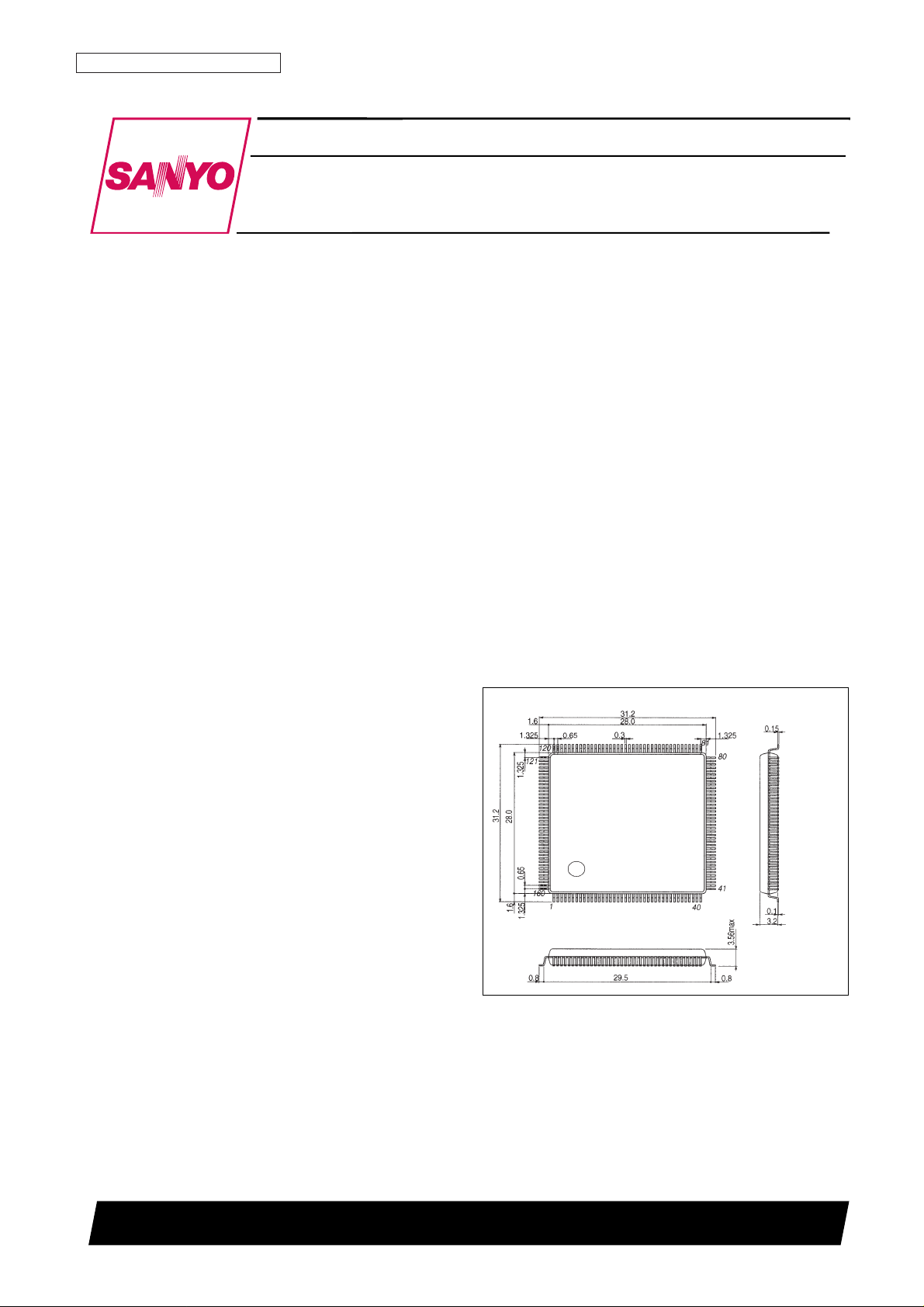
Package Dimensions
unit: mm
3153A-QFP160E
CMOS LSI
D1997RM (OT) No. 5784-1/7
Preliminaly
SANYO: QIP160E
[LC895925]
SANYO Electric Co.,Ltd. Semiconductor Bussiness Headquarters
TOKYO OFFICE Tokyo Bldg., 1-10, 1 Chome, Ueno, Taito-ku, TOKYO, 110-0005 JAPAN
Signal Processing LSI for CD-R Drives
LC895925
Ordering number : EN*5784
Page 2
No. 5784-2/7
LC895925
Parameter Symbol Conditions Ratings Unit
Maximum power supply voltage V
DD
max –0.3 to +7.0 V
I/O voltage V
I
, V
O
–0.3 to VDD+0.3 V
Maximum power dissipation Pd max Ta ≤ 70°C 600 mW
Operating temperature Topr –30 to +70 °C
Storage temperature Tstg –55 to +125 °C
Solder resistance 10 seconds 260 °C
Specifications
Maximum Ratings at Ta = 25°C, VSS= 0 V
Parameter Symbol Conditions
Ratings
Unit
min typ max
Input high level voltage V
IH
TTL levels, for pin types 1 and 6
2.2 V
Input low level voltage V
IL
0.8 V
Input high level voltage V
IH
TTL levels, for pin type 4, with pull-up resistors
2.2 V
Input low level voltage V
IL
0.8 V
Input high” level voltage V
IH
TTL levels, for pin 0 and 7, with Schmitt inputs
2.5 V
Input low level voltage V
IL
0.6 V
Output high level voltage V
OHIOH
= –2 mA, for pin type 3 VDD– 2.1 V
Output low level voltage V
OLIOL
= 2 mA, for pin type 3 0.4 V
Output high level voltage V
OHIOH
= -2 mA, for pin types 2, 4, and 6 VDD– 2.1 V
Output low level voltage V
OLIOL
= 2 mA, for pin types 2, 4, and 6 0.4 V
Output high level voltage V
OHIOH
= -48 mA, for pin type 7 VDD– 2.1 V
Output low level voltage V
OLIOL
= 48 mA, for pin type 7 0.4 V
Output low level voltage V
OLIOL
= 2 mA, for pin type 5 0.4 V
Input leak current I
IL
VI= VSS, VDD, for pin types 0, 1, 6, and 7 –10 +10 µA
Pull-up resistance R
UP
For pin types 4 and 5 40 80 160 kΩ
DC Characteristics at Ta = –30 to +70°C, VSS= 0 V, VDD= 4.5 to 5.5 V
Parameter Symbol Conditions
Ratings
Unit
min typ max
Supply voltage V
DD
4.5 5.0 5.5 V
Input voltage range V
IN
0 V
DD
V
Permissible Operating Range at Ta = –30 to +70°C, VSS= 0 V
The pin types above refer to the following groups.
Input
(0) BCK, BICLKIN, BIDATAI, C2PO, LOCKIN, LRCK, PLLOUTIN, ROUGH, SBSO, SCOR, SDATA, WFCK, CS,
RD, WR
(1) SUA0 to SUA6, TEST0 to TEST6, X1EN, RESET
Output
(2) CLV+, CLV–, FSW
(3) DATACKO, EFM, EFMG, EFMGATE0 to EFMGATE6, EXCK, LOCK, MCK, MON, PSUBSYNC, RA0 to RA9,
SUBSYNC, CAS0 to CAS1, RAS0 to RAS1, ERROR, EXTACK, FRCK, LWE, UWE, OE
Input/Output
(4) D0 to D7, IO0 to IO15
(5) INT0 to INT1, SWAIT
(6) ATIPSYNC, Reserve0 to Reserve5
(7) ACK, ATN, BSY, C/D, DB0 to DB7, DBP, I/O, MSG, REQ, RST, SEL
Note: The XTAL0, XTAL1, XTALCK0, and XTALCK1 pins fall outside of these DC characteristic specifications.
Page 3
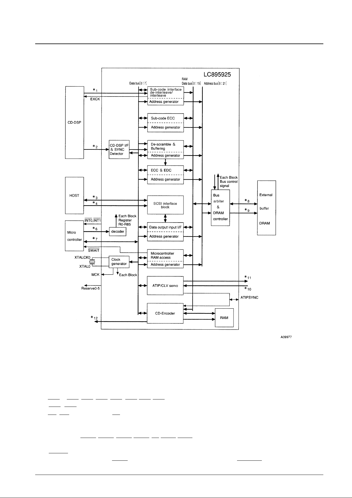
*1 WFCK, SBSO, SCOR
*2 BCK, SDATA, LRCK, C2PO
*3 DB0 to DB7, DBP, BSY, MSG, SEL, RST, REQ, I/O, C/D
*4 ACK, ATN
*6 RD, WR, SUA0 to SUA6, CS
*7 D0 to D7
*8 IO0 to IO15
*9 RA0 to RA9, RAS0, RAS1, CAS0, CAS1, OE, UWE, LWE
*10 PLLOUTIN, ROUGH, LOCKIN, BICLKIN, BIDATAIN
*11 ERROR, LOCK, CLV+(MDP), CLV–(MDS), MON, FSW
*12 SUBSYNC, PSUBSYNC, FRCK, EFM, EFMG, EFMGATE3 to EFMGATE0, EXTACK, DATACK0
Block Diagram
No. 5784-3/7
LC895925
Page 4

Pin Descriptions
No. 5784-4/7
LC895925
Type: I: Input pin, O: Output pin, B: Bidirectional pin, P: Power supply pin, N: No connection pin
Pin Number Pin Name Type Description
1 V
SS
P
2 Reserve0 B Reserved for future expansion (leave open)
3 Reserve1 B Reserved for future expansion (connect to ground)
4 Reserve2 B Reserved for future expansion (connect to ground)
5 TEST1 I Test pin (connect to V
SS
)
6 XTALCK0 I Crystal oscillator circuit input pin (17.2872 to 69.1488 MHz)
7 XTAL0 O Crystal oscillator circuit output pin
8 TEST2 I Test pin (connect to V
SS
)
9 MCK O Master Clock output pin
10 TEST3 I Test pin (connect to V
SS
)
11 XTALCK1 I Crystal oscillator circuit input pin (20 MHz)
12 XTAL1 O Crystal oscillator circuit output pin
13 TEST4 I Test pin (connect to V
SS
)
14 V
DD
P
15 V
SS
P
16 CLV
+
(MDP) O
17 CLV
–
(MDS) O
CLV servo signal output pins
18 MON O
19 FSW O
20 V
DD
P
21 V
SS
P
22 PLLOUTIN I Wobble signal carrier clock input pin
23 ROUGH I Rough CLV servo wobble signal input pin
24 LOCKIN I CD decoder lock signal input pin
25 LOCK O CLV servo lock monitor pin
26 ERROR O ATIP parity error detection pin
27 ATIPSYNC B ATIP synchronization signal I/O pin
28 BIDATAI I Biphase data input pin
29 BICLKIN I Biphase data transfer clock input pin
30 V
DD
P
31 IO0 B
32 IO1 B
33 IO2 B
34 IO3 B
35 IO4 B Data signal pins for ROM encoder/decoder buffer RAM, with pull-up resistors
36 IO5 B
37 IO6 B
38 IO7 B
39 IO8 B
40 V
DD
P
41 V
SS
P
Continued on next page.
Page 5

No. 5784-5/7
LC895925
Continued from preceding page.
Type: I: Input pin, O: Output pin, B: Bidirectional pin, P: Power supply pin, N: No connection pin
Pin Number Pin Name Type Description
42 IO9 B
43 IO10 B
44 IO11 B
45 IO12 B Data signal pins for ROM encoder/decoder DRAM, with pull-up resistors
46 IO13 B
47 IO14 B
48 IO15 B
49 V
SS
P
50 RA0 O
51 RA1 O
52 RA2 O
53 RA3 O
54 RA4 O
Address signal pins for ROM encoder/decoder DRAM
55 RA5 O
56 RA6 O
57 RA7 O
58 RA8 O
59 RA9 O
60 V
DD
P
61 V
SS
P
62 RAS0 O
DRAM RAS signal output pins
63 RAS1 O
64 CAS0 O
DRAM CAS signal output pins
65 CAS1 O
66 OE O DRAM Output Enable signal output pin
67 UWE O DRAM Output Upper Write Enable signal output pin
68 LWE O DRAM Output Lower Write Enable signal output pin
69 TEST0 I Test pin (connect to V
SS
)
70 V
DD
P
71 EXCK O Subcode data read shift clock output pin
72 WFCK I Subcode frame synchronization input pin
73 SBSO I Subcode serial data input pin
74 SCOR I Subcode block synchronization input pin
75 V
SS
P
76 BCK I Serial data input clock input pin
77 SDATA I Serial data input pin
78 LRCK I 44.1-kHz strobe signal input pin
79 C2PO I C2 pointer input pin
80 V
DD
P
81 V
SS
P
82 DB0 B
SCSI pins
83 DB1 B
84 V
DD
P
85 DB2 B
SCSI pins
86 DB3 B
87 VSS P
88 DB4 B
SCSI pins
89 DB5 B
Continued on next page.
Page 6

No. 5784-6/7
LC895925
Continued from preceding page.
Type: I: Input pin, O: Output pin, B: Bidirectional pin, P: Power supply pin, N: No connection pin
Pin Number Pin Name Type Description
90 V
DD
P
91 DB6 B SCSI pins
92 V
DD
P
93 V
SS
P
94 DB7 B
SCSI pins
95 DBP B
96 V
DD
P
97 V
SS
P
98 ATN B
SCSI pins
99 BSY B
100 V
DD
P
101 V
SS
P
102 ACK B
SCSI pins
103 RST B
104 V
DD
P
105 V
SS
P
106 MSG B
SCSI pins
107 SEL B
108 V
DD
P
109 C/D B SCSI pins
110 V
DD
P
111 REQ B
SCSI pins
112 I/O B
113 V
SS
P
114 X1EN I Pin for selecting SCSI interface clock (XTALCK0 or XTALCK1)
115 RESET I RESET pin
116 V
DD
P
117 DATACKO O 4.3218-MHz (Normal Speed) oscillator output pin
118 PSUBSYNC O Pseudo subcode synchronization output pin
119 EXTACK O ATIP synchronization interval acknowledgment output pin
120 V
DD
P
121 V
SS
P
122 SUBSYNC O Subcode synchronization signal output pin
123 FRCK O EFM frame synchronization signal output pin
124 FRCK O EFM output gate signal output pin
125 EFM O EFM signal output pin
126 EFMGATE0 O
127 EFMGATE1 O
EFM pulse width detection gate signals
128 EFMGATE2 O
129 EFMGATE3 O
130 TEST5 I Test pin (connect to V
SS
)
131 V
SS
P
132 TEST6 I Test pin (connect to V
SS
)
Continued on next page.
Page 7

PS No. 5784-7/7
LC895925
This catalog provides information as of December, 1997. Specifications and information herein are subject to
change without notice.
■ No products described or contained herein are intended for use in surgical implants, life-support systems, aerospace
equipment, nuclear power control systems, vehicles, disaster/crime-prevention equipment and the like, the failure of
which may directly or indirectly cause injury, death or property loss.
■ Anyone purchasing any products described or contained herein for an above-mentioned use shall:
➀ Accept full responsibility and indemnify and defend SANYO ELECTRIC CO., LTD., its affiliates, subsidiaries and
distributors and all their officers and employees, jointly and severally, against any and all claims and litigation and all
damages, cost and expenses associated with such use:
➁ Not impose any responsibility for any fault or negligence which may be cited in any such claim or litigation on
SANYO ELECTRIC CO., LTD., its affiliates, subsidiaries and distributors or any of their officers and employees
jointly or severally.
■ Information (including circuit diagrams and circuit parameters) herein is for example only; it is not guaranteed for
volume production. SANYO believes information herein is accurate and reliable, but no guarantees are made or implied
regarding its use or any infringements of intellectual property rights or other rights of third parties.
Continued from preceding page.
Type: I: Input pin, O: Output pin, B: Bidirectional pin, P: Power supply pin, N: No connection pin
Pin Number Pin Name Type Description
133 SUA0 I
134 SUA1 I
135 SUA2 I
136 SUA3 I Command register selection address input pinsI
137 SUA4 I
138 SUA5 I
139 SUA6 I
140 V
DD
P
141 V
SS
P
142 D0 B
143 D1 B
144 D2 B
145 D3 B
146 D4 B Microcontroller data signal pins, with pull-up resistors
147 D5 B
148 D6 B
149 D7 B
150 V
DD
P
151 CS I Chip select signal from microcontroller
152 RD I Data read signal from microcontroller
153 WR I Data write signal from microcontroller
154 SWAIT O Wait signal to microcontroller
155 INT0 O
Interrupt request signals to microcontroller. Open drain outputs with built-in pull-up resistors
156 INT1 O
157 Reserve3 B
158 Reserve4 B Reserved for future expansion (leave open)
159 Reserve5 B
160 V
DD
P
 Loading...