

Page 1
Ordering number : ENN6249A
13100TH (OT)/31599HA (OT) No. 6249-1/12
Overview
The LC895299W and LC895299L are CD-ROM drive
digital servo system ICs that integrate all signalprocessing functions after the RF head amplifier on a
single chip.
Functions
• Built-in digital servo and ATAPI (IDE) CD-ROM,
CD-DSP, CAV audio, and1-Mbit DRAM functions
Features
CD-DSP Block
• Supports full CAV operation at 48× speed
• Assures stable data readout by performing frame sync
signal detection, protection, and interpolation.
• Demodulates the EFM signal to produce 8-bit symbol
data.
• Applies a CRC check to the subcode Q signal and then
outputs that signal via parallel I/O to the system
microprocessor.
• Performs unscrambling and deinterleaving operations to
rearrange the demodulated EFM signal in the stipulated
order.
• Detects and corrects error signals and processes flags
(C1: 2 errors, C2: 4 errors)
• References the C1 flags and the C2 error check result to
set the C2 flags and interpolates or mutes the signal
depending on the C2 flags.
• Provides two types of muting: zero-cross muting and
soft muting.
• Independent left and right channel digital attenuators
(8-bit resolution)
Provides two types of attenuation: direct attenuation and
soft attenuation.
• Bilingual support
• Built-in digital audio interface (supports both CLV and
CAV)
• Built-in digital deemphasis
• Built-in 8× oversampling digital filters
• Built-in D/A converters
CD-ROM Decoder and ATAPI (IDE) Interface
Block
• Built-in ATAPI (IDE) interface
• The user can freely set the CD main channel, C2 flag,
and subcode areas in internal DRAM.
• Batch transfer function (Function for transferring the CD
main channel, C2 flag, or subcode data in a single
operation.)
• Multiple transfer function (Function for transferring
multiple blocks automatically in a single operation.)
• CAV audio functions
• Intelligent functions (auto buffering, auto decoding, and
CD-R functions)
• Subcode P to W buffering function (No ECC) and
CD-TEXT support
• Supports Ultra DMA MODE2, MODE1, and MODE0
• Built in 1-Mbit DRAM
LC895299W, 895299L
SANYO Electric Co.,Ltd. Semiconductor Company
TOKYO OFFICE Tokyo Bldg., 1-10, 1 Chome, Ueno, Taito-ku, TOKYO, 110-8534 JAPAN
48× Speed ATAPI (IDE) CD-ROM Decoder
with On-Chip Digital Servo System
CMOS IC
Any and all SANYO products described or contained herein do not have specifications that can handle
applications that require extremely high levels of reliability, such as life-support systems, aircraft’s
control systems, or other applications whose failure can be reasonably expected to result in serious
physical and/or material damage. Consult with your SANYO representative nearest you before using
any SANYO products described or contained herein in such applications.
SANYO assumes no responsibility for equipment failures that result from using products at values that
exceed, even momentarily, rated values (such as maximum ratings, operating condition ranges, or other
parameters) listed in products specifications of any and all SANYO products described or contained
herein.
Page 2
No. 6249-2/12
LC895299W, 895299L
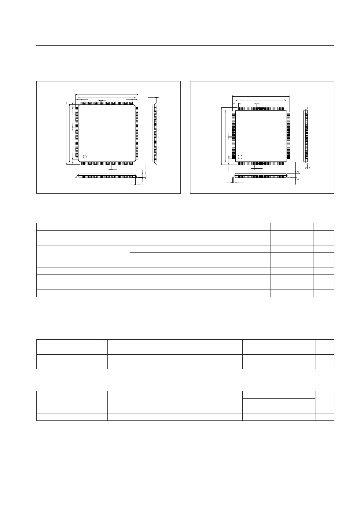
Package Dimensions
unit: mm
3230-SQFP176 3244-LQFP176
176
133
1
44
132
89
45
88
0.4
20.0
(1.4)
(0.5)
22.0
0.5
0.15
1.6max
0.4
20.0
(1.4)
22.0
0.1
(1.4)
0.125
SANYO: LQFP176
[LC895299L]
26.0
24.0
0.5
1.25
26.0
0.1
0.5
24.0
1.25
1
44
45
88
89
132
133
176
1.25
1.25
0.5
1.6max
1.4
0.2
0.5
0.125
SANYO: SQFP176
[LC895299W]
Parameter Symbol Conditions Ratings Unit
Maximum supply voltage
V
DD5
max Ta = 25°C –0.3 to +6.0 V
V
DD3
max Ta = 25°C –0.3 to +4.6 V
Input and output voltages
V
I5
, VO5Ta = 25°C –0.3 to V
DD5
+ 0.3 V
V
I3
, VO3Ta = 25°C –0.3 to V
DD3
+ 0.3 V
Allowable power dissipation Pd max Ta ≤ 70°C 550 mW
Operating temperature Topr –30 to +70 °C
Storage temperature Tstg –55 to +125 °C
Soldering conditions (pins only) 10 seconds 235 °C
Input and output power I
I
, I
O
±20 * mA
Specifications
Absolute Maximum Ratings at VSS= 0 V
Note: * Per single input or output basic cell.
Parameter Symbol Conditions
Ratings
Unit
min typ max
Supply voltage V
DD
4.5 5.0 5.5 V
Input voltage range V
IN
0V
DD
V
Allowable Operating Ranges at Ta = 0 to +70°C, VSS= 0 V
I/O Cell 5.0-V Power Supply
Parameter Symbol Conditions
Ratings
Unit
min typ max
Supply voltage V
DD
3.0 3.3 3.8 V
Input voltage range V
IN
0V
DD
V
Internal Cell 3.3-V Power Supply
Note: The input voltage range for speeds of 45× or over is 4.5 to 5.25 V.
Note: The input voltage range differs depending on the drive speed used. Contact your Sanyo representative for details.
Page 3

No. 6249-3/12
LC895299W, 895299L
Parameter Symbol Conditions Applicable pins *
Ratings
Unit
min typ max
Input high-level voltage V
IH
TTL level inputs 1
2.2 V
Input low-level voltage V
IL
0.8 V
Input high-level voltage V
IH
TTL level inputs with pull-up resistors 7
2.2 V
Input low-level voltage V
IL
0.8 V
Input high-level voltage V
IH
TTL level inputs with pull-down resistors 2
2.2 V
Input low-level voltage V
IL
0.8 V
Input high-level voltage V
IH
TTL level inputs
3, 9
2.4 V
Input low-level voltage V
IL
Schmitt inputs
0.8 V
Input high-level voltage V
IH
TTL level inputs
19, 20
2.4 V
Input low-level voltage V
IL
Schmitt inputs with pull-up resistors
0.8 V
Input high-level voltage V
IH
CMOS level inputs
4
0.8 V
DD
V
Input low-level voltage V
IL
Schmitt inputs
0.2 V
DD
V
Input high-level voltage V
IH
CMOS level inputs with pull-up resistors 5
0.7 V
DD
V
Input low-level voltage V
IL
0.3 V
DD
V
Analog input voltage V
ANI
18 1/4 V
DD
3/4 V
DD
V
Output high-level voltage V
OHIOH
= –2 mA
6, 17
VDD– 2.1 V
Output low-level voltage V
OLIOL
= 2 mA 0.4 V
Output high-level voltage V
OHIOH
= –8 mA
7, 8, 14
VDD– 2.1 V
Output low-level voltage V
OLIOL
= 8 mA 0.4 V
Output high-level voltage V
OHIOH
= –4 mA
9, 12, 10, 20
VDD– 2.1 V
Output low-level voltage V
OLIOL
= 24 mA 0.4 V
Output high-level voltage V
OHIOH
= –4 mA
16
VDD– 2.1 V
Output low-level voltage V
OLIOL
= 4 mA 0.4 V
Output low-level voltage V
OLIOL
= 24 mA 11, 21 0.4 V
Output low-level voltage V
OLIOL
= 1 mA 13 0.4 V
Output low-level voltage V
OLIOL
= 8 mA 15 0.4 V
Analog output voltage V
ANO
22 1/4 V
DD
3/4 V
DD
V
Input leakage current I
IL
VI= VSS, V
DD
1, 3, 4, 9 –10 +10 µA
Output leakage current I
OZ
During high-impedance output
9, 11, 13,
–10 +10 µA
14, 16, 17
Pull-up resistance R
UP
5 50 100 200 kΩ
Pull-up resistance R
UP
7, 15 20 40 80 kΩ
Pull-up resistance R
UP
19, 20, 21 7 10 13 kΩ
Pull-down resistance R
DN
2 50 100 200 kΩ
Pull-down resistance R
DN
10 7 10 13 kΩ
DC Characteristics at Ta = 0 to +70°C, VSS= 0 V, VDD= 4.5 to 5.5 V
Note: * The applicable pin column entries refer to the following sets.
INPUT
1 : ATPINSEL, SUA0 to SUA7
2 : TEST0 to TEST2
3 : DA0 to DA2, ZCS1FX, ZCS3FX, ZDIOR, ZDIOW, ZHRST, ZCS, ZRD, ZWR
4 : ZRESET, ZDSPRST
5 : FG
18 : AD0, AD1, PH, BH, RREC, FE, TE, VREF, CSS, AD2
19 : ZDMACK, CSEL
OUTPUT
6 : FSEQ
8 : HFLO, FSX, EFLG, C2F, WRQ, DIR, PCK, EFMOUT
13 : HINTRQ
11 : ZIOCS16
10 : DMARQ
13 : PDS1 to PDS3
14 : DOUT
15 : ZSWAIT, ZINT0, ZINT1
21 : IORDY
16 : DSLB, EQS, OUTPORT0 to OUTPORT2, MCK
17 : RHLD, TSH, BHH, GHS, LDON
22 : PHC, BHC, FBAL, TBAL, SGC, TOFST, TDO, FDO, SLDO, SPDO
INOUT
7 : D0 to D7, TRV, TRV2
9 : DD0 to DD15
20 : ZDASP, ZPDIAG
Note: XTAL, XTALCK
The above pins are not included in the DC Characteristics.
Page 4
No. 6249-4/12
LC895299W, 895299L
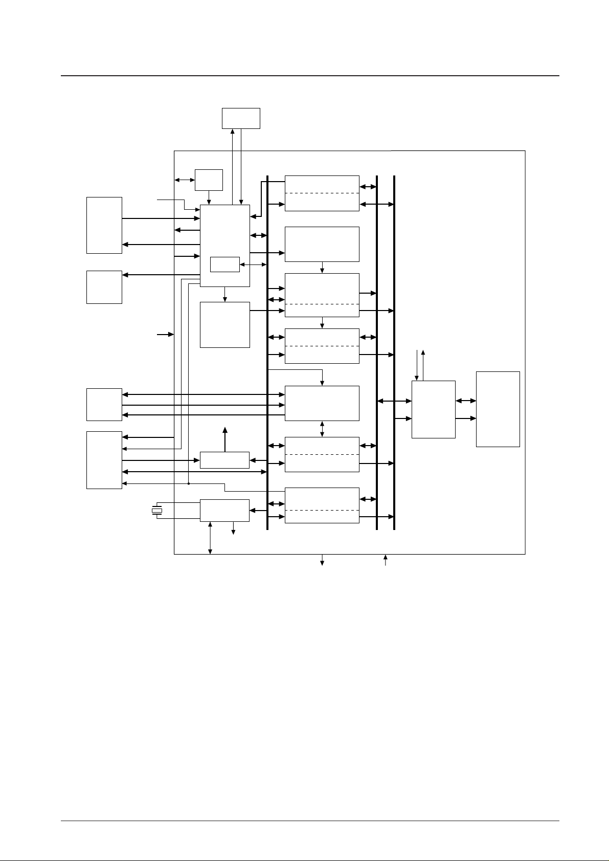
Block Diagram
Sub-code
SYNC
Detector
De-scramble
&
Buffering
Address generator
Micro controller
RAM access
Address generator
Address generator
ECC & EDC
I/F
ATAPI
Address generator
Data output input I/F
Address generator
CAV-AUDIO
Bus Arbiter
&
DRAM
controller
Buffer
DRAM
Each Block
Bus control
signal
Each Block
Register
CD-DSP I/F
&
SYNC
Detector
SRAM
CD-DSP
LA9238
HOST
Audio
Circuit
VCEC
PLL
Driver
FG
TDO, FDO
SLDO, SPDO
Micro
controller
decoder
PLL Clock
generator
*11
*1
*12
*2
*14
*3
*4
*5
*6
*7
*8
WRQ
ZSWAIT
ZINT 1
ZINT 0
ZRESET
ZDSPRST
*13
*9
*10
XTALCK
XTAL
Each Block
Data bus[0:7]
Address bus[0:18]
DRAM
Data bus[0:15]
A12530
*1 EFMIN, EFMIN2, PH, BH, FE, TE, TES, RREC
*2 RHLD, TSH, EQS, BHH, GHS, LDON, FBAL, TBAL, TOFST, SGC
*3 LOUT, ROUT, DOUT
*4 DD0 to DD15, ZDASP, ZPDIAG
*5 ZCS1FX, ZCS3FX, DA0 to DA2, ZDIOR, ZDIOW, ZDMACK, ZHRST, CSEL
*6 DMARQ, HINTRQ, ZIOCS16, IORDY
*7 ZRD, ZWR, ZCS, CSCTRL, SUA0 to SUA7
*8 D0 to D7
*9 DIR/FLOCK, HFLO/TLOCK, FSEQ, FSX/LRCK, EFLG/CK2, C2F, EFMOUT, PCK, TRV2/DATA, TRV, PORT OUT0 to OUT2
*10 ATPINSEL, TEST0 to TEST2
*11 RPO, OPP, PCKISTF, PCKISTP, PDO, POS1 to POS3, FR
*12 SLCO0 to SLCO3, JITC, DSLB, PHC, BHC
*13 PLL1 to PLL3
*14 SLCIT1 to SLCIT2, JITIN, AD0 to AD2, VREF, CSS
Page 5

No. 6249-5/12
LC895299W, 895299L
Pin Functions
LC895299 Pin Functions 1
(When pin 95, ATPINSEL, is low)
Type
I INPUT B BIDIRECTION NC NOT CONNECT
O OUTPUT P POWER
Pin No. Pin Type Function
1V
SS
P Logic system ground
2 FLOCK/CRCERR O
Monitor outputs
3 DIR/TLOCK O
4 ZSWAIT O Wait signal output to the microcontroller
5 WRQ/HFLO O Monitor output
6 ZINT0 O
Microcontroller interrupt
7 ZINT1 O
8 TEST0 I Test pin (Must be tied to ground during normal operation.)
9D0B
10 D1 B
11 D2 B
12 D3 B
13 D4 B Microcontroller data bus
14 D5 B
15 D6 B
16 D7 B
17 MCK O Clock output to the microcontroller
18 ZCS I Microcontroller ZCS signal
19 NC
20 NC
21 V
DDD
P DRAM VDD: 5 V
22 V
DD1
P 3.3 V
23 V
SS
P Logic system ground
24 V
SSD
P DRAM ground
25 NC
26 NC
27 SUA0 I
28 SUA1 I
29 SUA2 I
30 SUA3 I
Microcontroller address bus
31 SUA4 I
32 SUA5 I
33 SUA6 I
34 SUA7 I
35 ZWR I Microcontroller write signal
36 ZRD I Microcontroller read signal
37 FSEQ O Frame synchronization detection
38 DOUT/TESO O Digital output/tes output
39 V
DD0
P I/O system power supply: 5 V
40 V
SS
P Logic system ground
41 PLL1 I
42 PLL2 I System Clock PLL
43 PLL3 O
44 PLL1 V
DD
P Logic PLL VDD: 3.3 V
45 PLL1 V
SS
P Logic PLL system ground
46 CSEL I
47 ZHRST I
48 ZDASP B ATAPI I/F
49 ZCS3FX I
50 ZCS1FX I
51 V
SS1
I I/F ground
52 V
DD0
I I/O system power supply: 5 V
Continued on next page.
Page 6

No. 6249-6/12
LC895299W, 895299L
Continued from preceding page.
Pin No. Pin I/O Function
53 DA2 I
54 DA0 I
55 ZPDIAG B ATAPI I/F
56 DA1 I
57 ZIOCS16 O
58 V
SS1
P I/F ground
59 HINTRQ O
60 ZDMACK I
61 IORDY O
ATAPI I/F
62 ZDIOR I
63 ZDIOW I
64 DMARQ O
65 V
DD0
P I/O system power supply: 5 V
66 V
DD1
P 3.3 V
67 V
SS1
P I/F ground
68 DD15 B
69 DD0 B
70 DD14 B ATAPI I/F
71 DD1 B
72 DD13 B
73 V
SS1
P I/F ground
74 DD2 B
75 DD12 B
76 DD3 B ATAPI I/F
77 DD11 B
78 DD4 B
79 V
SS1
P I/F ground
80 DD10 B
81 DD5 B
82 DD9 B
ATAPI I/F
83 DD6 B
84 DD8 B
85 DD7 B
86 V
DD0
P I/O system power supply: 5 V
87 ROUT O D/A converter output
88 AUV
DD
P D/A converter VDD: 5 V
89 AUV
SS
P DAC ground
90 LOUT O D/A converter output
91 V
SS
P Logic system ground
92 XTAL O XTALCK output
93 XTALCK I XTALCK input (33.8688 MHz)
94 V
DD0
P I/O system power supply: 5 V
95 ATPINSEL I ATAPI pin assignment selection
96 TEST1 I Test pin (Must be tied to ground during normal operation.)
97 FSX/LRCK O
Monitor outputs
98 EFLG/CK2 O
99 TRV2/DATA B
General-purpose I/O ports
100 TRV B
101 C2F O C2F output
102 PCK O PCK output
103 EFMOUT O EFM output
104 OUTPORT0 O
105 OUTPORT1 O General-purpose output ports
106 OUTPORT2 O
107 NC
Continued on next page.
Page 7

No. 6249-7/12
LC895299W, 895299L
Continued from preceding page.
Pin No. Pin I/O Function
108 NC
109 V
SSD
P DRAM ground
110 V
DD1
P 3.3 V
111 V
SS
P Logic GND
112 V
DDD
P DRAM VDD: 5 V
113 NC
114 NC
115 DSLB O SLC PWM output
116 AV
DD
P Slice level VDD: 3.3 V
117 SLCIST1 I
EFM slice level setting
118 SLCIST2 I
119 SLCO0 O
120 SLCO1 O
EFM slice level outputs
121 SLCO2 O
122 SLCO3 O
123 EFMIN I
EFM input
124 EFMIN2 I
125 AV
SS
P Slice level ground
126 JITIN I Jitter detection input
127 JITC O Jitter output
128 RPO O
P/N balance adjustment
129 OPP I
130 PCKISTF I Frequency comparator charge pump setting
131 PCKISTP I Phase comparator charge pump setting
132 PLL2V
DD
P VCEC PLL VDD: 3.3 V
133 PLL2V
SS
P VCEC PLL ground
134 PDO O Charge pump filter
135 PDS1 O
136 PDS2 O Charge pump selection
137 PDS3 O
138 FR I VCO frequency setting
139 SV
SS
P Servo system ground
140 AD0 I A/D converter input 0
141 AD1 I A/D converter input 1
142 PH I Peak hold circuit
143 BH I Bottom hold circuit
144 RREC I Optical recognition input
145 FE I FE input
146 TE I TE input
147 TES I TES comparator input
148 VREF I VREF input
149 CSS I Center servo input
150 AD2 I A/D converter input 2
151 PHC O PH slice capacitor connection
152 BHC O BH slice capacitor connection
153 FBAL O Focus balance
154 SV
DD
P Servo system VDD: 5V
155 SV
SS
P Servo system ground
156 TBAL O Tracking balance
157 SGC O Servo gain adjustment
158 TOFST O Tracking offset adjustment
159 TDO O Tracking output
160 FDO O Focus output
161 SLDO O Sled output
162 SPDO O Spindle output
Continued on next page.
Page 8

No. 6249-8/12
LC895299W, 895299L
All NC pins must be left open.
Pins whose name begin with Z operate with inverted (negative) logic.
Applications must supply 5 V to V
DD0
, 3.3 V to V
DD1
, the 1-bit D/A converter 5 V to AUVDD, the logic PLL 3.3 V to PLL1VDD, the VCEC PLL 3.3 V to
PLL2V
DD
, the slice level 3.3 V to AVDD, the servo system 5 V to SVDD, and the DRAM 5 V to V
DDD
.
V
SS
is the logic system ground, AUVSSis the 1-bit D/A converter ground, V
SS1
is the IDE interface driver ground, PLL1VSSis the logic PLL ground, PLL2V
SS
is the VCEC PLL ground, AVSSis the slice level ground, SVSSis the servo system ground, and V
SSD
is the DRAM ground.
Continued from preceding page.
Pin No. Pin I/O Function
163 V
DD0
P A/D and D/A converter VDD: 5 V
164 V
SS
P Logic ground
165 V
DD1
P 3.3 V
166 RHLD O RF AGC hold output
167 TSH O TS frequency switching
168 EQS O RF equalizer selection
169 BHH O BH frequency switching
170 GHS O RF and TS signal gain switching
171 LDON O Laser control
172 TEST2 I Test pin (Must be tied to ground during normal operation.)
173 FG I FG input
174 ZDSPRST I DSP RESET
175 ZRESET I CHIP RESET
176 V
DD0
P I/O system VDD: 5 V
Page 9

No. 6249-9/12
LC895299W, 895299L
Pin Functions
LC895299 Pin Functions 2
(When pin 95, ATPINSEL, is high)
Type
I INPUT B BIDIRECTION NC NOT CONNECT
O OUTPUT P POWER
Pin No. Pin Type Function
1V
SS
P Logic system ground
2 FLOCK/CRCERR O
Monitor outputs
3 DIR/TLOCK O
4 ZSWAIT O Wait signal output to the microcontroller
5 WRQ/HFLO O Monitor output
6 ZINT0 O
Microcontroller interrupt
7 ZINT1 O
8 TEST0 I Test pin (Must be tied to ground during normal operation.)
9D0B
10 D1 B
11 D2 B
12 D3 B
13 D4 B
Microcontroller data bus
14 D5 B
15 D6 B
16 D7 B
17 MCK O Clock output to the microcontroller
18 ZCS I Microcontroller ZCS signal
19 NC
20 NC
21 V
DDD
P DRAM VDD: 5 V
22 V
DD1
P 3.3 V
23 V
SS
P Logic system ground
24 V
SSD
P DRAM ground
25 NC
26 NC
27 SUA0 I
28 SUA1 I
29 SUA2 I
30 SUA3 I
Microcontroller address bus
31 SUA4 I
32 SUA5 I
33 SUA6 I
34 SUA7 I
35 ZWR I Microcontroller write signal
36 ZRD I Microcontroller read signal
37 FSEQ O Frame synchronization detection
38 DOUT/TESO O Digital output/tes output
39 V
DD0
P I/O system power supply: 5 V
40 V
SS
P Logic system ground
41 PLL1 I
42 PLL2 I System Clock PLL
43 PLL3 O
44 PLL1 V
DD
P Logic PLL VDD: 3.3 V
45 PLL1 V
SS
P Logic PLL ground
46 CSEL I
47 DD7 B
48 DD8 B ATAPI I/F
49 DD6 B
50 DD9 B
51 V
SS1
P I/F ground
52 V
DD0
P I/O system power supply: 5 V
Continued on next page.
Page 10

No. 6249-10/12
LC895299W, 895299L
Continued from preceding page.
Pin No. Pin I/O Function
53 DD5 B
54 DD10 B
55 DD4 B ATAPI I/F
56 DD11 B
57 DD3 B
58 V
SS1
P I/F GND
59 DD12 B
60 DD2 B
61 DD13 B
ATAPI I/F
62 DD1 B
63 DD14 B
64 DD0 B
65 V
DD0
P I/O system power supply: 5 V
66 V
DD1
P 3.3 V
67 V
SS1
P I/F GND
68 DD15 B
69 DMARQ O
70 ZDIOW I ATAPI I/F
71 ZDIOR I
72 IORDY O
73 V
SS1
P I/F GND
74 ZDMACK I
75 HINTRQ O
76 ZIOCS16 O ATAPI I/F
77 DA1 I
78 ZPDIAG B
79 V
SS1
P I/F GND
80 DA0 I
81 DA2 I
82 ZCS1FX I
ATAPI I/F
83 ZCS3FX I
84 ZDASP B
85 ZHRST I
86 V
DD0
P I/O system power supply: 5 V
87 ROUT O D/A converter output
88 AUV
DD
P D/A converter VDD: 5 V
89 AUV
SS
P DAC ground
90 LOUT O D/A converter output
91 V
SS
P Logic system ground
92 XTAL O XTALCK output
93 XTALCK I XTALCK input (33.8688 MHz)
94 V
DD0
P I/O system power supply: 5 V
95 ATPINSEL I ATAPI pin assignment selection
96 TEST1 I Test pin (Must be tied to ground during normal operation.)
97 FSX/LRCK O
Monitor outputs
98 EFLG/CK2 O
99 TRV2/DATA B
General-purpose I/O ports
100 TRV B
101 C2F O C2F output
102 PCK O PCK output
103 EFMOUT O EFM output
104 OUTPORT0 O
105 OUTPORT1 O General-purpose output ports
106 OUTPORT2 O
107 NC
Continued on next page.
Page 11

No. 6249-11/12
LC895299W, 895299L
Continued from preceding page.
Pin No. Pin I/O Function
108 NC
109 V
SSD
P DRAM ground
110 V
DD1
P 3.3 V
111 V
SS
P Logic system ground
112 V
DDD
P DRAM VDD: 5 V
113 NC
114 NC
115 DSLB O SLC PWM output
116 AV
DD
P Slice level VDD: 3.3 V
117 SLCIST1 I
EFM slice level setting
118 SLCIST2 I
119 SLCO0 O
120 SLCO1 O
EFM slice level outputs
121 SLCO2 O
122 SLCO3 O
123 EFMIN I
EFM input
124 EFMIN2 I
125 AV
SS
P Slice level ground
126 JITIN I Jitter detection input
127 JITC O Jitter output
128 RPO O
P/N balance adjustment
129 OPP I
130 PCKISTF I Frequency comparator charge pump setting
131 PCKISTP I Phase comparator charge pump setting
132 PLL2V
DD
P VCEC PLL VDD: 3.3 V
133 PLL2V
SS
P VCEC PLL ground
134 PDO O Charge pump filter
135 PDS1 O
136 PDS2 O Charge pump selection
137 PDS3 O
138 FR I VCO frequency setting
139 SV
SS
P Servo system ground
140 AD0 I A/D converter input 0
141 AD1 I A/D converter input 1
142 PH I Peak hold circuit
143 BH I Bottom hold circuit
144 RREC I Optical recognition input
145 FE I FE input
146 TE I TE input
147 TES I TES comparator input
148 VREF I VREF input
149 CSS I Center servo input
150 AD2 I A/D converter input 2
151 PHC O PH slice capacitor connection
152 BHC O BH slice capacitor connection
153 FBAL O Focus balance
154 SV
DD
P Servo system VDD: 5V
155 SV
SS
P Servo system ground
156 TBAL O Tracking balance
157 SGC O Servo gain adjustment
158 TOFST O Tracking offset adjustment
159 TDO O Tracking output
160 FDO O Focus output
161 SLDO O Sled output
162 SPDO O Spindle output
Continued on next page.
Page 12

PS No. 6249-12/12
LC895299W, 895299L
This catalog provides information as of January, 2000. Specifications and information herein are subject
to change without notice.
Specifications of any and all SANYO products described or contained herein stipulate the performance,
characteristics, and functions of the described products in the independent state, and are not guarantees
of the performance, characteristics, and functions of the described products as mounted in the customer’s
products or equipment. To verify symptoms and states that cannot be evaluated in an independent device,
the customer should always evaluate and test devices mounted in the customer’s products or equipment.
SANYO Electric Co., Ltd. strives to supply high-quality high-reliability products. However, any and all
semiconductor products fail with some probability. It is possible that these probabilistic failures could
give rise to accidents or events that could endanger human lives, that could give rise to smoke or fire,
or that could cause damage to other property. When designing equipment, adopt safety measures so
that these kinds of accidents or events cannot occur. Such measures include but are not limited to protective
circuits and error prevention circuits for safe design, redundant design, and structural design.
In the event that any or all SANYO products (including technical data, services) described or contained
herein are controlled under any of applicable local export control laws and regulations, such products must
not be exported without obtaining the export license from the authorities concerned in accordance with the
above law.
No part of this publication may be reproduced or transmitted in any form or by any means, electronic or
mechanical, including photocopying and recording, or any information storage or retrieval system,
or otherwise, without the prior written permission of SANYO Electric Co., Ltd.
Any and all information described or contained herein are subject to change without notice due to
product/technology improvement, etc. When designing equipment, refer to the “Delivery Specification”
for the SANYO product that you intend to use.
Information (including circuit diagrams and circuit parameters) herein is for example only; it is not
guaranteed for volume production. SANYO believes information herein is accurate and reliable, but
no guarantees are made or implied regarding its use or any infringements of intellectual property rights
or other rights of third parties.
All NC pins must be left open.
Pins whose name begin with Z operate with inverted (negative) logic.
Applications must supply 5 V to V
DD0
, 3.3 V to V
DD1
, the 1-bit D/A converter 5 V to AUVDD, the logic PLL 3.3 V to PLL1VDD, the VCEC PLL 3.3 V to
PLL2V
DD
, the slice level 3.3 V to AVDD, the servo system 5 V to SVDD, and the DRAM 5 V to V
DDD
.
V
SS
is the logic system ground, AUVSSis the 1-bit D/A converter ground, V
SS1
is the IDE interface driver ground, PLL1VSSis the logic PLL ground, PLL2V
SS
is the VCEC PLL ground, AVSSis the slice level ground, SVSSis the servo system ground, and V
SSD
is the DRAM ground.
Continued from preceding page.
Pin No. Pin I/O Function
163 V
DD0
P A/D and D/A converter VDD: 5 V
164 V
SS
P Logic system ground
165 V
DD1
P 3.3 V
166 RHLD O RF AGC hold output
167 TSH O TS frequency switching
168 EQS O RF equalizer selection
169 BHH O BH frequency switching
170 GHS O RF and TS signal gain switching
171 LDON O Laser control
172 TEST2 I Test pin (Must be tied to ground during normal operation.)
173 FG I FG input
174 ZDSPRST I DSP RESET
175 ZRESET I CHIP RESET
176 V
DD0
P I/O system VDD: 5 V
 Loading...