

Page 1

Overview
The LC895297 is a single-chip CD-ROM decoder and
CD-DSP system that supports full CAV 20× operation and
includes a built-in ATA-PI (IDE) interface.
Functions
• Full CAV 20× CD-DSP and CD-ROM decoder
functions with built-in ATA-PI (IDE) interface
Features
[CD-ROM Decoder and ATA-PI (IDE) Interface Blocks]
• Full CAV 20×operation
• ATA-PI (IDE) interface
• Supports the use of EDO DRAM.
• Supports the use of up to 4 Mbits of buffer RAM.
• The user can set up arbitrary CD main channel and C2
flag areas in buffer RAM.
• Batch transfer function (function that automatically
transfers the CD main channel and C2 flag data in a
single operation.)
• Multi-block transfer function (function that
automatically transfers multiple blocks in a single
operation.)
• DVD ECC interface
• Intelligent functions
[CD-DSP Block]
• The IC inputs a high-frequency signal, slices that signal
at the correct level, converts that result to an EFM coded
signal, and compares the phase with that of the built-in
VCO.
• Uses an external 16.9344-MHz crystal element to
generate a standard clock and to correctly generate the
required internal timings.
• Performs frame synchronization, signal detection,
protection, and insertion, and assures stable data
readout.
• Demodulates the EFM coded signal to produce 8-bit
symbol data.
• After applying a CRC check to the subcode Q signal,
outputs that signal to a microprocessor over a parallel
I/O channel.
• Performs unscrambling and de-interleaving to reorder
the demodulated EFM signal in the prescribed manner.
• Performs error code detection and correction, and flag
processing. (C1: dual errors, C2: four errors)
• Sets the C2 flags based on the C1 flags and a C2 check,
and performs interpolation or muting depending on the
C2 flags. Adopts a 2-point interpolation circuit, and
converges the signal to the muting level if the C2 flags
indicate over 2 consecutive uncorrectable errors.
• Accepts the input of commands from a control
microprocessor over an 8-bit parallel interface. Supports
track jump, disc motor start/stop, muting on/off, and
track counting commands.
• Can perform arbitrary track counts.
• Includes CAV audio functions.
• Adopts zero-cross muting.
• Includes 8×oversampling digital filters.
• D/A converter with PWM output.
• Includes independent left and right channel digital
attenuators.
• Provides digital deemphasis.
• Supports bilingual functions.
Package Dimensions
unit: mm
3230-SQFP176
CMOS LSI
22898HA (OT) No. 5785-1/9
Preliminary
SANYO: SQFP176
[LC897297]
SANYO Electric Co.,Ltd. Semiconductor Bussiness Headquarters
TOKYO OFFICE Tokyo Bldg., 1-10, 1 Chome, Ueno, Taito-ku, TOKYO, 110-0005 JAPAN
Full CAV 20× CD-ROM Decoder with
Built-in ATA-PI (IDE) Interface and CD-DSP
LC895297
Ordering number : EN*5785
Page 2
No. 5785-2/9
LC895297
Parameter Symbol Conditions Ratings Unit
Maximum supply voltage V
DD
max –0.3 to +7.0 V
Input and output voltage V
I
, V
O
–0.3 to VDD+0.3 V
Allowable power dissipation Pd max Ta ≤ 70°C *1 500 mW
Operating temperature Topr –30 to +70 °C
Storage temperature Tstg –55 to +125 °C
Soldering conditions (pins only) 10s 235 °C
Input and output current I
I
, I
O
Per individual input or output cell ±20 mA
Note 1: Applications that use this IC must adopt heat dissipation measures, such as the insertion of a thermally conductive sheet.
Specifications
Absolute Maximum Ratings at Ta = 25°C, VSS= 0 V
Parameter Symbol Conditions
Ratings
Unit
min typ max
[Input and Output Cell Power Supply]
Supply voltage V
DD
4.5 5.0 5.5 V
Input voltage range V
IN
0 V
DD
V
[Internal Cell Power Supply]
Supply voltage V
DD
3.9 4.0 4.1 V
Input voltage range V
IN
0 V
DD
V
Allowable Operating Ranges at Ta = –30 to +70°C, VSS= 0 V
Parameter Symbol Conditions
Ratings
Unit
min typ max
Input high-level voltage V
IH
TTL levels. Applicable pins: (10) and (13)
2.2 V
Input low-level voltage VIL 0.8 V
Input high-level voltage V
IH
TTL levels. Applicable pins: (1) 2.2 V
Input low-level voltage V
IL
Pull-up resistor included. 0.8
Input high-level voltage V
IH
TTL levels. Applicable pins: (2), (3), and (15) 2.4 V
Input low-level voltage V
IL
Schmitt inputs. 0.8 V
Input high-level voltage V
IH
CMOS levels: Applicable pins: (14) 0.7 V
DD
V
Input low-level voltage V
IL
0.3 V
DD
V
Input high-level voltage V
IH
CMOS levels: Applicable pins: (4) 0.8 V
DD
V
Input low-level voltage V
IL
Schmitt inputs. 0.2 V
DD
V
Output high-level voltage V
OH
IOH= –2 mA: Applicable pins: (5), (1), (9),
V
DD
– 2.1 V
(10), and (15)
Output low-level voltage V
OL
IOL= 2 mA: Applicable pins: (5), (1), (9),
0.4 V
(10), and (15)
Output high-level voltage V
OHIOH
= –4 mA: Applicable pins: (3) and (6) V
DD
– 2.1 V
Output low-level voltage V
OLIOL
= 24 mA: Applicable pins: (3) and (6) 0.4 V
Output low-level voltage V
OLIOL
= 2 mA: Applicable pins: (7) and (11) 0.4 V
Output low-level voltage V
OLIOL
= 24 mA: Applicable pins: (12) 0.4 V
Input leakage current I
IL
VI= VSS, VDD: Applicable pins: (2), (3), (4),
–10 +10 µA
(10), and (15)
Output leakage current I
OZ
In high-impedance output mode: Applicable
–10 +10 µA
pins: (3), (6), (7), (9), (10), (12), and (15)
Pull-up resistance R
UP
Applicable pins: (1) and (11) 40 80 160 kΩ
Electrical Characteristics at Ta = –30 to +70°C, VSS= 0 V, VDD= 4.5 to 5.5 V
The applicable pin sets are as follows:
[INPUT]
(2) ZRESET, ZDMACK, ZHRST, DA0to DA2, ZCS1FX, ZCS3FX, ZDIOR, ZDIOW, FG
(4) ZCSCTRL, ZCS, ZRD, ZWR, HFL, TES
(14) DEFI
(13) SUA0 o SUA6
[OUTPUT]
(6) DMARQ, HINTRQ
(5) RA0 to RA8, ZRAS0, ZCAS0, ZOE, ZUWE, ZLWE, C2F, ROMXA, FSX, EFLG, PCK, FSEQ, TOFF, TGL, 4.2M, WRQ, RWC, COIN, ZCQCK, RCHP,
RCHN, LCHP, LCHN
(7) ZRSTCPU, ZRSTIC
(9) JP
+
, JP–, SPO
(11) ZINT0, ZINT1, ZSWAIT
(12) IORDY, ZIOCS16
Continued on next page.
Page 3
No. 5785-3/9
LC895297
[INOUT]
(1) D0 to D7, IO0 to IO15
(3) DD0 to DD15, ZDASP, ZPDIAG
(10) IOP0 to IOP7
(15) DRESP, DREQ
Note: XTAL, XTALCK, R0, VCNT0, PDO0, R1, VCNT1, PO11, PO21, BSN1, R2, VCNT2, PO12, PO22, and BSN2
The above pins are not covered by the electrical characteristics.
The 1-bit D/A converter block pins are only measured using a logic tester; no analog measurements are performed.
Continued from preceding page.
Parameter Symbol Conditions
Ratings
Unit
min typ max
Input high-level voltage V
IH
Micro-signal amplifier. Applicable pins: EFMI
3.2 V
Input low-level voltage V
IL
1.8 V
Output high-level voltage V
OH
IOH= –4 mA. Applicable pins:
V
DD
– 2.1 V
EFMO and ZEFMO
Output low-level voltage V
OL
IOL= 4 mA. Applicable pins:
0.4 V
EFMO and ZEFMO
Input leakage current I
IL
VI= VSS, VDD: Applicable pins: EFMI –10 +10 µA
Output leakage current I
OZ
In high-impedance mode: Applicable pins:
–10 +10 µA
EFMO and ZEFMO
Electrical Characteristics at Ta = –30 to +70°C, VSS= 0 V, VDD= 4.5 to 5.5 V
EFM Input and Output Signals
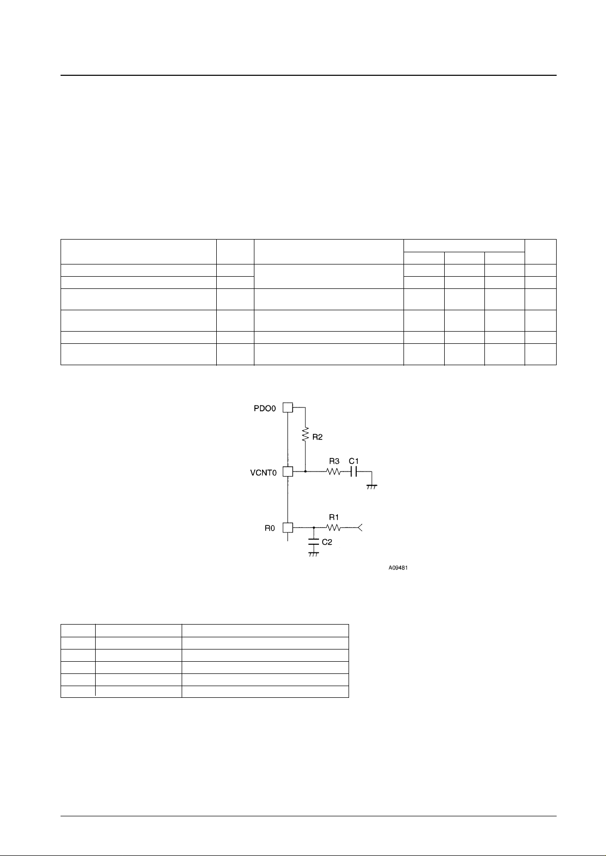
External Clock Generator PLL Circuit
Figure 1 PLL Circuit
While the circuit structure is fixed, the values of the components will vary with the circuit board capacitance and other application circuit parameters.
Symbol Currently used value Notes
R1 7.5 kΩ VCO adjustment resistor
R2 10 kΩ Low-pass filter resistor
R3 200 Ω Low-pass filter phase compensation resistor
C1 0.1 µF Low-pass filter capacitor
C2 0.1 µF VCO bias stabilization capacitor
Page 4

No. 5785-4/9
LC895297
Block Diagram
*1 DEFI, EFMI, HFL, TES
*2 4.2M, EFMO, PCK, FSEQ, TOFF, TGL, JP
+
, JP–, RWC, COIN, ZCQCK
*3 RCHP, RCHN, LCHP, LCHN
*4 DD0 to DD15, ZDASP, ZPDIAG
*5 ZCS1FX, ZCS3FX, DA0 to DA2, ZDIOR, ZDIOW, ZDMACK, ZHRST
*6 DMARQ, HINTRQ, ZIOCS16, IORDY
*7 ZRD, ZWR, ZCS, ZCSCTRL, SUA0 to SUA6
*8 D0 to D7
*9 IO0 to IO15
*10 RA0 to RA8, ZRAS0, ZCAS0, ZOE, ZUWE, ZLWE
*11 DREQ
*12 DRESP
*13 IOP0 to IOP7
*14 R0, VCNT0, PDO0
**1 HISIDE (WD25C32) is made by WESTERN DIGITAL
DVD interface
IDE interface
External
buffer
RAM
Page 5

Pin Functions
I : Input pin, O: Output pin, B : Bidirectional pin, P: Power supply pin, NC: Not connected
No. 5785-5/9
LC895297
Pin No. Pin name Type Function
1 AV
SS0
P
2 R0 I VCO bias resistor connection
3 VCNT0 I VCO control voltage input
4 PDO0 O Charge pump output
5 TEST0 I
Test pins
6 TEST1 I
7 IOP0 (HDB7) B
8 IOP1 (HDB6) B
9 IOP2 (HDB5) B
10 IOP3 (HDB4) B General-purpose I/O ports
11 IOP4 (HDB3) B These pins are used for DVD ECC data input when the DVD interface is used.
12 IOP5 (HDB2) B
13 IOP6 (HDB1) B
14 IOP7 (HDB0) B
15 V
DD2
P 4.0 V
16 TEST3 I Test pin
17 TEST4 I Test pin
18 DRESP I DVD ECC data latch signal input
19 DREQ O DVD ECC data request output
20 RCHP O 1-bit D/A converter right channel P output
21 RCHN O 1-bit D/A converter right channel N output
22 V
DD1
P 1-bit D/A converter left and right channel power supply
23 V
SS1
P 1-bit D/A converter right channel ground
24 LCHP O 1-bit D/A converter left channel P output
25 LCHN O 1-bit D/A converter left channel N output
26 V
SS0
P
27 XTALCK I Crystal oscillator circuit input (16.9344 MHz)
28 XTAL O Crystal oscillator circuit output
29 V
SS0
P
30 NC
31 ZRSTCPU O CPU reset signal output
32 ZRSTIC O Drive IC reset signal output
33 ZRESET I IC reset input
34 D7 B
35 D6 B
36 D5 B
37 D4 B Microcontroller data signal connection.
38 D3 B These pins include built-in pull-up resistors.
39 D2 B
40 D1 B
41 D0 B
Continued on next page.
Page 6

No. 5785-6/9
LC895297
Continued from preceding page.
I : Input pin, O: Output pin, B : Bidirectional pin, P: Power supply pin, NC: Not connected
Pin No. Pin name Type Function
42 SUA0 I
Microcontroller register selection
43 SUA1 I
44 V
DD0
P 5 V
45 V
SS0
P
46 V
DD2
P 4.0 V
47 SUA2 I
48 SUA3 I
49 SUA4 I Microcontroller register selection
50 SUA5 I
51 SUA6 I
52 ZCSCTRL I Microcontroller chip select active-low/high selection
53 ZCS I Register chip select signal input (from the microcontroller)
54 ZSWAIT O Wait signal output (to the microcontroller)
55 ZWR I Data write signal input (from the microcontroller)
56 ZRD I Data read signal input (from the microcontroller)
57 ZINT0 O
Interrupt request signal output (to the microcontroller)
58 ZINT1 O
59 WRQ O Subcode Q output standby output
60 FSEQ O Synchronization signal detection output
61 C2F O C2 flag output for ROMXA
62 ROMXA O Interpolation data output for ROMXA
63 FSX (CK2) O 7.35-kHz signal output (Bit clock output for ROMXA)
64 EFLG (LRSY) O C1 and C2 error correction monitor output (LRSY output for ROMXA)
65 FG I FG pulse input for CAV control
66 V
DD2
P 4.0 V
67 V
SS0
P
68 TEST2 I Test pin
69 ZEFMO O Inverted EFM signal output
70 EFMO O EFM signal output
71 EFMI I EFM signal input
72 V
DD0
P 5 V
73 JP– O
Track jump output
74 JP+ O
75 TGL O Tracking gain switching output
76 TOFF O Tracking off output
77 TES I Tracking error signal input. Schmitt input
78 HFL I Tracking detection signal input. Schmitt input
79 NC
80 SPO O CAV control output
81 DEFI I Defect detection signal input
82 4.2M O 4.2336-MHz output
83 R1 I VCO bias resistor connection
84 BSN1 I Charge pump bias resistor connection
85 VCNT1 I VCO control voltage
86 PO11 O
Charge pump outputs
87 PO21 O
88 AV
DD1
P 4.0 V
89 AV
SS1
P
Continued on next page.
Page 7

No. 5785-7/9
LC895297
Continued from preceding page.
I : Input pin, O: Output pin, B : Bidirectional pin, P: Power supply pin, NC: Not connected
Pin No. Pin name Type Function
90 R2 I VCO bias resistor connection
91 BSN2 I Charge pump bias resistor connection
92 VCNT2 I VCO control voltage
93 PO12 O
Charge pump outputs
94 PO22 O
95 V
DD2
P 4.0 V
96 PCK O EFM data reproduction bit clock monitor
97 NC
98 ZCQCK O ASP command acquisition clock output
99 COIN O ASP command output
100 RWC O Output to the ASP read/write control input
101 ZRAS0 O Buffer RAM RAS signal output
102 ZCAS0 O Buffer RAM CAS signal output
103 ZOE O Buffer RAM output enable
104 V
SS0
P
105 ZUWE O Buffer RAM upper write enable
106 ZLWE O Buffer RAM lower write enable
107 RA0 O
108 RA1 O Data buffer RAM address signal outputs
109 RA2 O
110 V
DD0
P 5 V
111 V
SS0
O
112 RA3 O
113 RA4 O
114 RA5 O
Data buffer RAM address signal outputs
115 RA6 O
116 RA7 O
117 RA8 O
118 IO8 B
Data buffer RAM data input and output
119 IO9 B
These pins include built-in pull-up resistors.
120 IO10 B
121 V
SS0
P
122 IO11 B
123 IO12 B
124 IO13 B
125 IO14 B
126 IO15 B Data buffer RAM data input and output
127 IO7 B These pins include built-in pull-up resistors.
128 IO6 B
129 IO5 B
130 IO4 B
131 IO3 B
132 V
DD2
P 4.0 V
133 V
SS0
P
134 IO2 B
Data buffer RAM data input and output
135 IO1 B
These pins include built-in pull-up resistors.
136 IO0 B
Continued on next page.
Page 8

No. 5785-8/9
LC895297
Continued from preceding page.
I : Input pin, O: Output pin, B : Bidirectional pin, P: Power supply pin, NC: Not connected
Pin No. Pin name Type Function
137 ZHRST I ATAPI control signal
138 V
SS2
P
139 DD7 B ATAPI data bus
140 DD8 B
141 DD6 B
142 DD9 B
143 V
DD0
P 5 V
144 V
SS2
P
145 DD5 B ATAPI data bus
146 DD10 B
147 DD4 B
148 DD11 B
149 V
SS2
P
150 DD3 B ATAPI data bus
151 DD12 B
152 DD2 B
153 DD13 B
154 V
DD0
P 5 V
155 V
SS2
P
156 DD1 B ATAPI data bus
157 DD14 B
158 DD0 B
159 DD15 B
160 V
SS2
P
161 DMARQ O ATAPI control signal
162 ZDIOW I
163 ZDIOR I
164 IORDY O
165 ZDMACK I
166 HINTRQ O
167 ZIOCS16 O
168 V
SS2
P
169 DA1 I ATAPI control signal
170 ZPDIAG B
171 DA0 I
172 DA2 I
173 ZCS1FX I
174 ZCS3FX I
175 ZDASP B
176 AV
DD0
P 4.0 V
Pin names that start with the letter Z are negative-logic signals.
The following power-supply voltages must be provided; V
DD0
: 5 V, V
DD1
(for the 1-bit D/A converter): 5 V, and V
DD2
: 4.0 V.
V
SS0
is the logic system ground, V
SS1
is the 1-bit D/A converter ground, and VSS2 is the IDE interface drive ground.
Page 9

PS No. 5785-9/9
LC895297
Thermal Design
Since this IC supports operation at up to 20× speeds, it operates at extremely high speeds internally. Applications must
take measures to dissipate the heat that results from this high-speed operation. IC operation is not guaranteed if adequate
heat dissipation measures are not taken.
Heat Dissipation Example
Applications must be designed with a thermally conductive sheet above the LC895297 and the LC895297 positioned so
that the system chassis contacts the thermally conductive sheet.
This catalog provides information as of February, 1998. Specifications and information herein are subject to
change without notice.
■ No products described or contained herein are intended for use in surgical implants, life-support systems, aerospace
equipment, nuclear power control systems, vehicles, disaster/crime-prevention equipment and the like, the failure of
which may directly or indirectly cause injury, death or property loss.
■ Anyone purchasing any products described or contained herein for an above-mentioned use shall:
➀ Accept full responsibility and indemnify and defend SANYO ELECTRIC CO., LTD., its affiliates, subsidiaries and
distributors and all their officers and employees, jointly and severally, against any and all claims and litigation and all
damages, cost and expenses associated with such use:
➁ Not impose any responsibility for any fault or negligence which may be cited in any such claim or litigation on
SANYO ELECTRIC CO., LTD., its affiliates, subsidiaries and distributors or any of their officers and employees
jointly or severally.
■ Information (including circuit diagrams and circuit parameters) herein is for example only; it is not guaranteed for
volume production. SANYO believes information herein is accurate and reliable, but no guarantees are made or implied
regarding its use or any infringements of intellectual property rights or other rights of third parties.
Steel plate
Thermally conductive sheet
 Loading...