

Page 1
Ordering number : EN4272C
O2095HA (OT)/12395TH (OT)/ 61394TH No. 4272-1/6
Overview
The LC89515K is a version of the LC8951 in which
certain aspects of the internal registers have been
improved to make them even easier to use in CD-ROM
and CD-I products. The basic blocks are identical to those
in the LC8951 and these products are software and pin
compatible. Thus this product can replace the LC8951
without change. (However, this product is provided in a
slightly different package: a short lead type QIP-80E as
opposed to the QIP-80A.)
The LC89515K is an error correction and host interface
LSI for use in CD-ROM and CD-I products. This product
integrate in a single chip all CD-ROM specific functions,
including the error correction that was previously
implemented in software on a microprocessor and the CD
player and host computer interfaces that were previously
implemented in discrete components or gate arrays. The
use of the LSI can provide significant improvements in
CD-ROM and CD-I players, including increased transfer
rates, miniaturization, increased reliability, an improved
cost performance ratio, and a more efficient development
period.
Features
• Software and pin compatibility with the LC8951
(Changes were made to internal registers, the SRAM
interface, and other aspects.)
• Support for CD-ROM (mode 1) and CD-I (mode 2,
forms 1 and 2)
• All CD-ROM/CD-I special functions implemented on a
single chip
• Hardware error detection and correction for high speed,
without relying on software
• Real-time error correction: Error correction and
detection are possible without interrupting the host
interface bus.
• Fast transfers: up to 2.3 MB/s (18.4 Mb/s)
• Support for low-speed hosts (multiple block buffering)
• Built-in host interface command FIFO (for easy SCSI
support)
• Built-in 12-byte status FIFO
• CMOS circuits, single 5 V power supply
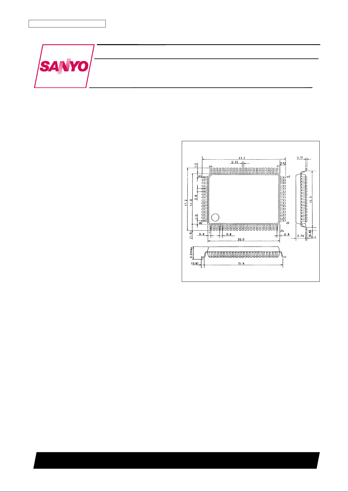
Package Dimensions
unit: mm
3174-QFP80E
SANYO: QIP80E
[LC89515K]
LC89515K
SANYO Electric Co.,Ltd. Semiconductor Bussiness Headquarters
TOKYO OFFICE Tokyo Bldg., 1-10, 1 Chome, Ueno, Taito-ku, TOKYO, 110-8534 JAPAN
CD-ROM/CD-I Error Correction/
Host Interface LSI
CMOS LSI
Page 2
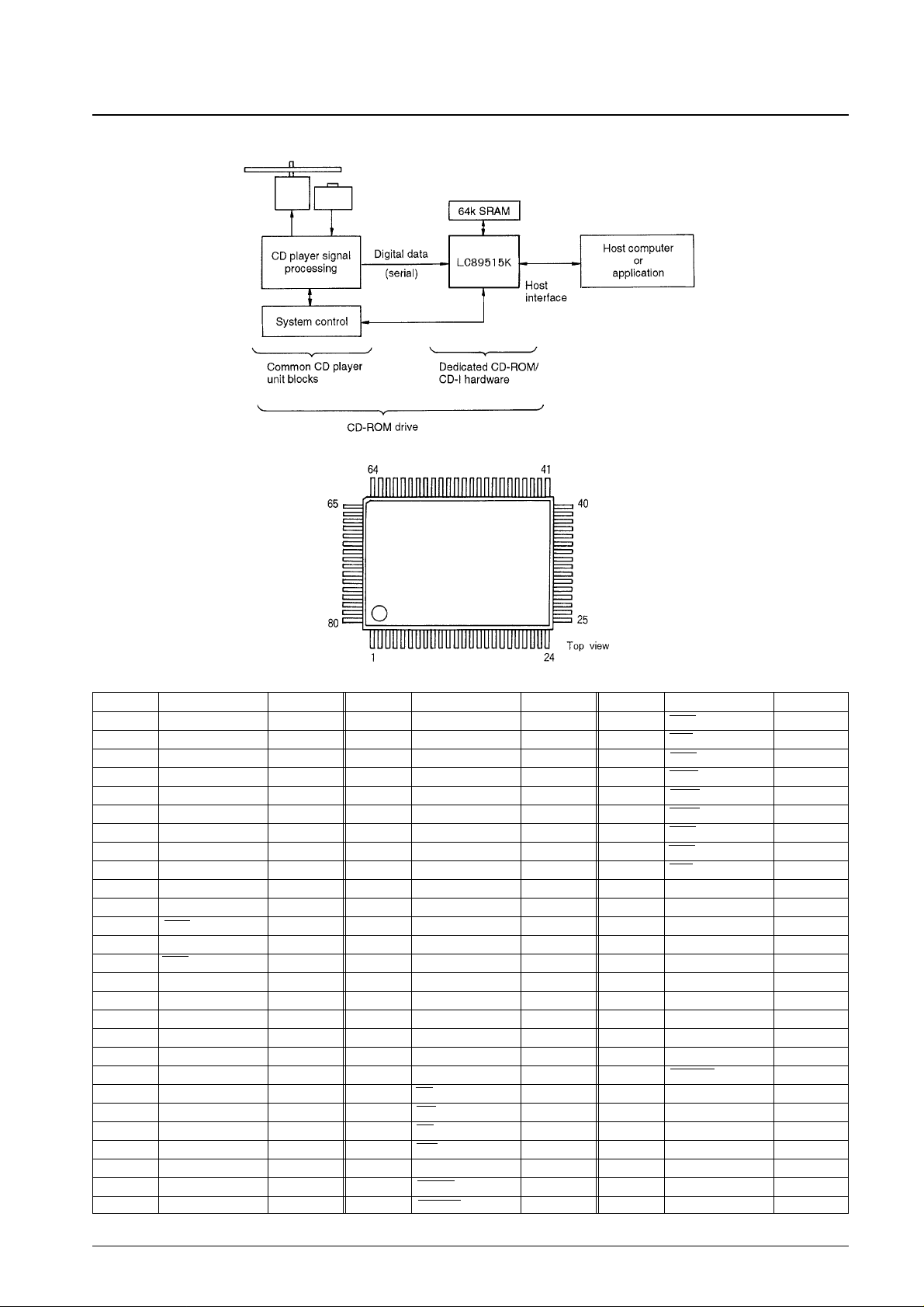
System Block Diagram
Pin Assignment
Type: I: Input pin, O: Output pin, B: Bidirectional pin, P: Power supply pin, NC: No connection
Note: Do not leave any of the V
DD
or VSSpins open. All of the VDDand VSSpins must be connected to ground or the power supply, respectively.
No. 4272-2/6
LC89515K
Pin No. Pin Type Pin No. Pin Type Pin No. Pin Type
1 V
SS
P 28 TEST2 I 55 HWR I
2 RA6 O 29 CSEL I 56 HRD I
3 RA7 O 30 LMSEL I 57 CMD I
4 RA8 O 31 V
DD
P 58 WAIT O
5 RA9 O 32 LRCK I 59 DTEN O
6 RA10 O 33 SDATA I 60 STEN O
7 RA11 O 34 BCK I 61 EOP O
8 RA12 O 35 C4LR I 62 RCS O
9 RA13 O 36 C2PO I 63 HDE O
10 RA14 O 37 MCK O 64 V
SS
P
11 RA15 O 38 D0 B 65 HD7 B
12 RWE O 39 D1 B 66 HD6 B
13 V
SS
P 40 D2 B 67 HD5 B
14 ROE O 41 V
SS
P 68 HD4 B
15 ERA B 42 D3 B 69 HD3 B
16 IO8 B 43 D4 B 70 HD2 B
17 IO7 B 44 D5 B 71 HD1 B
18 IO6 B 45 D6 B 72 HD0 B
19 IO5 B 46 D7 B 73 V
DD
P
20 IO4 B 47 RS I 74 SELDRQ I
21 IO3 B 48 RD I 75 RA0 O
22 IO2 B 49 WR I 76 RA1 O
23 IO1 B 40 CS I 77 RA2 O
24 V
SS
P 51 INT O 78 RA3 O
25 XTALCK I 52 V
SS
P 79 RA4 O
26 XTAL O 53 RESET I 80 RA5 O
27 TEST1 I 54 ENABLE I
Page 3

Block Functions
The LC89515K consist of three major blocks. This section describes those blocks.
1. CD Player Interface and Data Input Block
This LSI can handle three serial input formats selectable by setting external pin voltages. That is, differences in CD
player serial data formats can be compensated for by setting the CSEL and LMSEL inputs.
Internal operations are synchronized with the input data in block (sector) units using a synchronization detector
circuit. The synchronization circuit not only uses pattern detection on the externally input data, but also performs
synchronization protection with a synchronization signal interpolation circuit. These two synchronization systems
can be turned on or off under program control.
The input data is written to a buffer RAM in 8-bit units after passing through a descrambling circuit. The C2 pointer
(error flag) from the CD player is also written to RAM at this time. Although applications that use the C2 pointer
must provide a 9-bit RAM, the C2 pointer may be omitted and such applications need only provide an 8-bit RAM.
However, note that erasure correction cannot be performed if the C2 pointer is not used.
All input data, including sync, header, subheader and parity (2352 bytes) is stored in RAM in the order received from
the CD player in its entirety.
Furthermore, the LC89515K provides an output pin (MCK) for use with the CD LSI’s oscillator input pin. Therefore,
the number of oscillator elements in the end product can be reduced by selecting the LC89515K master clock
frequency to be twice the CD LSI clock frequency.
2. Error Detection and Correction Block
Error correction code decoding is performed after a full block (sector: 2352 bytes) of data has been stored in RAM.
The LC89515K error correction function operates in real time completely internally. The system software merely
waits for that processing to complete. Furthermore, buffering of data from the CD and transfer to the host computer
are performed simultaneously. That is, the LC89515K can transfer to the host computer data that has been error
corrected without any reduction in the data transfer rate from the CD.
The error correction technique not only consists of error detection and correction, but also supports combination with
erasure correction referencing the C2 pointer. This means that data with high reliability is acquired. The error
detection and correction process can correct single symbol errors, and can correct two symbol errors when combined
with erasure correction.
Furthermore, the error correction algorithm is programmable, and the LC89515K can be instructed to perform a wide
variety of procedures, such as iterative correction or QP/PQ correction, to improve data reliability.
After decoding the error correction codes (ECC), a 32-bit CRC error check is performed using the error detection
codes (EDC). During the CRC check the header and subheader are loaded into LC89515K internal registers.
After completing the CRC check the LC89515K issues a decoding complete interrupt to the control microprocessor.
The microprocessor then reads the header and subheader of the decoded block, the start address of the block in buffer
RAM, and a decoding result status indicator from the LC89515K.
3. Host Interface Block
The data transfer rate to the host computer has been improved significantly, to 2.3 MB/s, and since the amount of
buffering RAM has been increased to 64 kB, up to 27 sectors (blocks) of the CD ROM drive can be stored. This
memory can also be used as a disk cache memory.
The host interface provides an 8-byte FIFO for receiving commands from the host. The host can write up to 8 bytes
of commands at one time by asserting the HWR signal. When the host writes to the FIFO, the LC89515K issues a
command interrupt to the control microprocessor. Here, the commands written to the 8-byte FIFO are never
interpreted by the LC89515K.
When transferring data to the host, the control microprocessor writes the number of bytes to transfer and the start
address in buffer RAM of the block to be transferred. Then, it performs a write operation to the transfer start trigger
register. This causes the DTEN pin to go low and informs the host of the data transfer start. While the DTEN pin is
low the host reads data items one after another by generating HRD read pulses. If the host reads extremely rapidly,
i.e., over about 2.3 MB/s, then the LC89515K will output a WAIT signal. The host must not set HRD high while
WAIT is low. During this single block transfer operation, the microprocessor does nothing other than waiting for the
transfer complete interrupt that occurs when the transfer is done.
No. 4272-3/6
LC89515K
Page 4

Furthermore, the LC89515K SELDRQ pin can be used to perform DRQ (data request) transfers. This is a technique
in which transfers are performed by the host outputting HRD pulses according to a data request signal output from
the LC89515K and is similar to DMA controller operation.
When the last byte of the count specified by the control microprocessor is read, EOP goes active while the read pulse
is output. Also DTEN is set inactive after this time. Next, a transfer complete interrupt is issued to inform the control
microprocessor that the transfer to the host has completed.
The LC89515K control microprocessor can pass the decoding result for the data requested by the host and the CDROM drive status information to the host by writing to the LC89515K internal status registers. The status registers
are a 12-byte FIFO, and the host reads out data while the STEN signal is low. The STEN signal goes high when the
last byte is read. The LC89515K has nothing to do with the content of the status registers.
Since the command and status registers are neither interpreted nor executed by the LC89515K, the LC89515K user
can define the command and status data as unrestricted protocols between the host and the microprocessor. This
allows CD-ROM application systems to be designed without restriction, and also allows an existing system to be
replaced by a system using the LC89515K.
4. Points Common to All Blocks
The LC89515K performs data input and decoding at the same time in a pipelined manner. Also, writes of input data
to the buffer RAM, writes of data to be decoded, and reads to the buffer RAM for transfers to the host all proceed at
the same time with synchronization always being maintained by the LC89515K. Therefore there is no need for the
control microprocessor to be concerned with which master (system block) is accessing the buffer RAM.
5. Register Table
Read
Note: The values of the shaded bits are ignored.
No. 4272-4/6
LC89515K
RS AR No. Symbol BIT7 BIT6 BIT5 BIT4 BIT3 BIT2 BIT1 BIT0
0 — — AR 0 0 0 0 A
3
A
2
A
1
A
0
0000 R0 COMIN msb — — — — — — lsb
0001 R1 IFSTAT CMDI DTEI DECI 1 DTBSY STBSY DTEN STEN
0010 R2 DBCL B
7
B
6
B
5
B
4
B
3
B
2
B
1
B
0
0011 R3 DBCH DTEI DTEI DTEI DTEI B
11
B
10
B
9
B
8
0100 R4 HEAD0 msb — — — — — — lsb
0101 R5 HEAD1 msb — — — — — — lsb
0110 R6 HEAD2 msb — — — — — — lsb
1
0111 R7 HEAD3 msb — — — — — — lsb
1000 R8 PTL A
7
A
6
A
5
A
4
A
3
A
2
A
1
A
0
1001 R9 PTH A
15
A
14
A
13
A
12
A
11
A
10
A
9
A
8
1010 R10 WAL A
7
A
6
A
5
A
4
A
3
A
2
A
1
A
0
1011 R11 WAH A
15
A
14
A
13
A
12
A
11
A
10
A
9
A
8
1100 R12 STAT0 CRCOK ILSYNC NOSYNC LBLK WSHORT SBLK ERABLK UCEBLK
1101 R13 STAT1 MINERA SECERA BLKERA MODERA SH0ERA SH1ERA SH2ERA SH3ERA
1110 R14 STAT2 RMOD3 RMOD2 RMOD1 RMOD0 MODE NOCOR RFORM1 RFORM0
1111 R15 STAT3 VALST WLONG CBLK
Page 5

Write
Note: The values of the shaded bits are ignored.
6. Additional Registers
Write
[R14] CTRL2: Control 2
STENCTL (STEN control)
0.........The external STEN pin goes to 0 when the microprocessor writes one byte of status information. (This is
identical to LC8951 operation.)
1.........The external STEN pin goes to 0 due to 0 being written to the STENTRG register when the
microprocessor writes * bytes of status information.
This bit is set to 0 on reset.
STENTRG (STEN trigger)
This bit is only valid when STENCTL is 1.
The external STEN pin goes to 0 when a 0 is written to this bit.
This bit is reset when the host reads the last byte, i.e., when the external STEN pin has become 1.
DLAEN (drive last address enable)
When WRRQ is set to 0 during buffering, buffering continues until the next SYNC signal arrives and then stops.
This results in the sectors that are buffered when WRRQ was set to 0 becoming valid. (This bit is set to 0 on
reset.)
BCKSL (bit clock select)
Setting this bit to 1 allows the bit clock from the CD-DSP to be inverted. (SDATA is acquired on the rising edge
of BCK.) (This bit is set to 0 on reset.)
No. 4272-5/6
LC89515K
RS AR No. Symbol BIT7 BIT6 BIT5 BIT4 BIT3 BIT2 BIT1 BIT0
0 — — AR A
3
A
2
A
1
A
0
0000 R0 SBOUT msb — — — — — — lsb
0001 R1 IFCTRL CMDIEN DTEIEN DECIEN CMDBK DTWAI STWAI DOUTEN SOUTEN
0010 R2 DBCL B
7
B
6
B
5
B
4
B
3
B
2
B
1
B
0
0011 R3 DBCH B
11
B
10
B
9
B
8
0100 R4 DACL A
7
A
6
A
5
A
4
A
3
A
2
A
1
A
0
0101 R5 DACH A
15
A
14
A
13
A
12
A
11
A
10
A
9
A
8
0110 R6 DTTRG
1
0111 R7 DTACK
1000 R8 WAL A
7
A
6
A
5
A
4
A
3
A
2
A
1
A
0
1001 R9 WAH A
15
A
14
A
13
A
12
A
11
A
10
A
9
A
8
1010 R10 CTRL0 DECEN E01RQ AUTORQ ERAMRQ WRRQ QRQ PRQ
1011 R11 CTRL1 SYIEN SYDEN DSCREN COWREN MODRQ FORMRQ MBCKRQ SHDREN
1100 R12 PTL A
7
A
6
A
5
A
4
A
3
A
2
A
1
A
0
1101 R13 PTH A
15
A
14
A
13
A
12
A
11
A
10
A
9
A
8
1110 R14 CTRL2 0 0 0 BCKSL DLAEN 0 STENCTL STENTRG
1111 R15 RESET
Page 6

No. 4272-6/6
LC89515K
Specifications
Absolute Maximum Ratings at VSS= 0 V
Allowable Operating Ranges at Ta = –30 to +70°C, VSS= 0 V
Electrical Characteristics
DC Characteristics at Ta = –30 to +70°C, VSS= 0 V, VDD= 4.5 to 5.5 V
This catalog provides information as of February, 1997. Specifications and information herein are subject to
change without notice.
■ No products described or contained herein are intended for use in surgical implants, life-support systems, aerospace
equipment, nuclear power control systems, vehicles, disaster/crime-prevention equipment and the like, the failure of
which may directly or indirectly cause injury, death or property loss.
■ Anyone purchasing any products described or contained herein for an above-mentioned use shall:
➀ Accept full responsibility and indemnify and defend SANYO ELECTRIC CO., LTD., its affiliates, subsidiaries and
distributors and all their officers and employees, jointly and severally, against any and all claims and litigation and all
damages, cost and expenses associated with such use:
➁ Not impose any responsibility for any fault or negligence which may be cited in any such claim or litigation on
SANYO ELECTRIC CO., LTD., its affiliates, subsidiaries and distributors or any of their officers and employees
jointly or severally.
■ Information (including circuit diagrams and circuit parameters) herein is for example only; it is not guaranteed for
volume production. SANYO believes information herein is accurate and reliable, but no guarantees are made or implied
regarding its use or any infringements of intellectual property rights or other rights of third parties.
Parameter Symbol Conditions Ratings Unit
Maximum supply voltage V
DD
max Ta = 25°C –0.3 to +7.0 V
I/O voltages V
I
, VOTa = 25°C –0.3 to VDD+ 0.3 V
Allowable power dissipation Pd max Ta ≤ 70°C 350 mW
Operating temperature Topr –30 to +70 °C
Storage temperature Tstg –55 to +125 °C
Soldering temperature 10 seconds 260 °C
Parameter Symbol Conditions min typ max Unit
Supply voltage V
DD
4.5 5.0 5.5 V
Input voltage range V
IN
0 V
DD
V
Parameter Symbol Conditions min typ max Unit
Input high level voltage V
IH1
All input pins except those in (1) below and XTALCK
2.2 V
Input low level voltage V
IL1
0.8 V
Input high level voltage V
IH2
(1)
RESET (Schmitt trigger), RD, WR, HRD, HWR,
2.5 V
Input low level voltage V
IL2
CMD, CS, ENABLE and all bus pins
0.6 V
Output high level voltage V
OHIOH
= –2 mA 2.4 V
Output low level voltage V
OL1IOL
= 2 mA 0.4 V
Output low level voltage V
OL2IOL
= 2 mA
(2) INT (open drain circuit
0.4 V
with pull-up resistor)
Input leakage current I
L
VI= VSS, VDD: All input pins –25 +25 µA
Pull-up resistance R
UP
All bus pins, INT 10 20 40 kΩ
All output pins(including the
bus pins) except those in (2)
below and XTAL
 Loading...