

Page 1
Overview
The LC895126 is a CD-ROM decoder that in addition to
CD-ROM functions also provides a built-in SCSI
interface.
Functions
• CD-ROM ECC functions, subcode read function, SCSI
interface, CAV audio functions
Features
• Built-in SCSI interface (Includes a SCAM selection
register)
• Supports 24× playback and a 10MB/sec data transfer
rate (when 16-bit data path 70-ns EDO DRAM is used).
• Supports the use of up to 4 Mbit of buffer RAM.
• Users can freely set up the CD main channel, C2 flag,
and other areas in buffer RAM.
• Batch transfer function (Function that transfers the CD
main channel, C2 flag, and other data in a single
operation)
• Multiblock transfer function (Function that transfers
multiple blocks automatically in a single operation)
• Subcode ECC functions and CD-Text support
• CAV audio functions
• Intelligent functions (Including auto buffering, auto
decoding, and CD-R support)
• Supports 20MB/s transfers (This capability is currently
under evaluation (July 1997) and cannot be guaranteed
at present.)
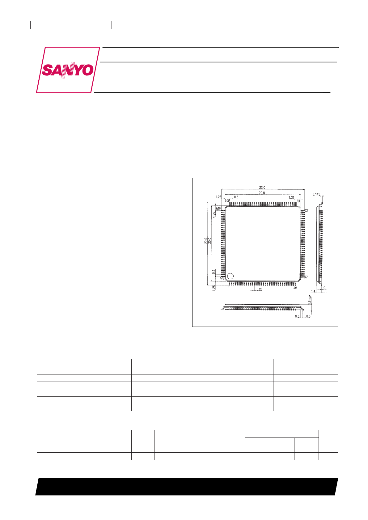
Package Dimensions
unit: mm
3214-SQFP144
CMOS LSI
13098HA (OT) No. 5786-1/7
Preliminary
SANYO: SQFP144
[LC895126]
SANYO Electric Co.,Ltd. Semiconductor Bussiness Headquarters
TOKYO OFFICE Tokyo Bldg., 1-10, 1 Chome, Ueno, Taito-ku, TOKYO, 110-0005 JAPAN
CD-ROM Decoder with Built-in SCSI Interface
LC895126
Ordering number : EN*5786
Parameter Symbol Conditions Ratings Unit
Maximum supply voltage V
DD
max –0.3 to +7.0 V
Input and output voltage V
I
, V
O
–0.3 to VDD+0.3 V
Allowable power dissipation Pd max Ta ≤ 70°C 550 mW
Operating temperature Topr –30 to +70 °C
Storage temperature Tstg –55 to +125 °C
Soldering conditions (pins only) 10 seconds 260 °C
Specifications
Absolute Maximum Ratings at Ta = 25°C, VSS= 0 V
Parameter Symbol Conditions
Ratings
Unit
min typ max
Supply voltage V
DD
4.5 5.0 5.5 V
Input voltage range V
IN
0V
DD
V
Allowable Operating Ranges at Ta = –30 to +70°C, VSS= 0 V
Page 2
No. 5786-2/7
LC895126
Parameter Symbol Conditions
Ratings
Unit
min typ max
Input high-level voltage V
IH
1
TTL level pins: (1)
2.2 V
Input low-level voltage V
IL
1 0.8 V
Input high-level voltage V
IH
2 TTL level pins: (9) 2.2 V
Input low-level voltage V
IL
2 Pins with built-in pull-up resistors. 0.8 V
Input high-level voltage V
IH
3 TTL level pins: (2) 2.2 V
Input low-level voltage V
IL
3 Schmitt input pins 0.8 V
Input high-level voltage V
IH
4 CMOS level pins: (3) 0.8 V
DD
V
Input low-level voltage V
IL
4 Schmitt input pins 0.2 V
DD
V
Input high-level voltage V
IH
5
(4), (8), (10)
2.0 V
Input low-level voltage V
IL
5 0.8 V
Output high-level voltage V
OH
1 IOH1 = –12 mA : (6) VDD– 2.1 V
Output low-level voltage V
OL
1 IOL1 = 12 mA : (6) 0.4 V
Output high-level voltage V
OH
2 IOH2 = –8 mA : (7) 2.4 V
Output low-level voltage V
OL
2 IOL2 = 8 mA : (7) 0.4 V
Output high-level voltage V
OH
2 IOH2 = –2 mA : (9), (5) 2.4 V
Output low-level voltage V
OL
2 IOL2 = 2 mA : (9), (5) 0.4 V
Output low-level voltage V
OL
4 IOL4 = 48 mA : (10) 0.4 V
Input leakage current I
IL
VI= VSSor VDD: All input pins. –25 +25 µA
Pull-up resistance R
UP
(5), (9) 60 120 240 kΩ
Electrical Characteristics at Ta = –30 to +70°C, VSS= 0 V, VDD= 4.5 to 5.5 V
The pin sets referred to above are as follows:
INPUT
(1) TEST0 to TEST4, CSCTRL, SUA0 to SUA6, X1EN, WFCK, SBS0
(2) C2PO, SDATA, BCK, LRCK, SCOR, ZRESET
(3) ZCS, ZRD, ZWR
(4) SCSISEL, XTALSEL
OUTPUT
(5) ZINT0, ZINT1, ZSWAIT
(6) MCK, MCK2, MCK3
(7) EXCK, DSDATA, DLRCK, DBCK, ZRAS0, ZRAS1, ZCAS0, ZCAS1, ZOE, ZUWE, ZLWE, RA0 to RA8
INOUT
(8) ACK, ATN
(9) D0 to D7, IO0 to IO15, IOP0 to IOP4
(10) DB0 to DB7, DBP, BSY, I/O, MSG, SEL, RST, REQ, C/D
Note: The XTAL0, XTALCK0, XTAL1, and XTALCK1 pins are not covered by the electrical characteristics.
Parameter Symbol Conditions
Ratings
Unit
min typ max
Input threshold voltage
V
t + t1VDD
= 4.50 to 5.50 V 1.60 2.00 V
V
t – t1
0.80 1.10 V
Hysteresis ∆V
tt1VDD
= 5.0 V 0.41 0.5 V
SCSI Interface Pin Input Characteristics
Parameter Symbol Conditions
Ratings
Unit
min typ max
Output high-level voltage V
OHIOH
= –24 mA 2.5 V
Output low-level voltage V
OLIOL
= 48 mA 0.4 V
Active Negation Output Characteristics
Note: Active negation refers to the DB0 to DB7, REQ, and DBPB outputs.
Figure 1
Page 3
No. 5786-3/7
LC895126
Pin Functions
I: Input pin, O: Output pin, B: Bidirectional pin, P: Power Supply pin, NC: Not Connection pin
Pin No. Symbol Type Function
1 V
SS0
P
2 IO2 B
Buffer RAM data I/O pins.
3 IO1 B
Built in pull-up resistors.
4 IO0 B
5 MCK2SEL I
Provided for switching between MCK2 (22 MHz, 20 MHz) and MCK3 (27 MHz, 25 MHz) in PLL mode.
Currently, must be connected to V
DD
.
6 NC
7 V
SS0
P
8 V
SS0
P
9 V
SS0
P
10 NC
11 NC
12 C2PO I
13 SDATA I
CD DSP interface
14 BCK I
15 LRCK I
16 EXCK O
Subcode I/O
17 WFCK I
18 V
DD
P
19 V
SS0
P
20 SBSO I
Subcode I/O
21 SCOR I
22 DSDATA O
23 DLRCK O D/A converter outputs
24 DBCK O
25 MCK O Outputs the XTALCK1 state (1/1, 1/2, or stopped)
26 V
SS0
P
27 XTALCK0 I Crystal oscillator circuit input
28 XTAL0 O Crystal oscillator circuit input
29 TEST0 I
30 TEST1 I
31 TEST2 I Test pins. These pins must be connected to V
SS0
.
32 TEST3 I
33 TEST4 I
34 MCK2 O
Outputs the XTALCK0 state (1/1, 1/2, 1/512, or stopped)
35 MCK3 O
36 V
SS0
P
37 V
DD
P
38 ZRESET I Chip reset. The system is reset by a low-level input.
39 ZRD I Microcontroller data read signal input
40 ZWR I Microcontroller data write signal input
Continued on next page.
Page 4

No. 5786-4/7
LC895126
Continued from preceding page.
Pin No. Symbol Type Function
41 ZCS I Register chip select signal input from the microcontroller
42 CSCTRL I CS active low/active high selection input from the microcontroller
43 SUA0 I
44 SUA1 I
45 SUA2 I
46 SUA3 I Microcontroller register selection signals
47 SUA4 I
48 SUA5 I
49 SUA6 I
50 D0 B
51 D1 B
Microcontroller data signals
52 D2 B
53 D3 B
54 V
DD
P
55 V
SS0
P
56 D4 B
57 D5 B
58 D6 B
59 D7 B
60 ZINT0 O Interrupt request signal output to the microcontroller (ECC side. Set up by register settings.)
61 ZINT1 O Interrupt request signal output to the microcontroller (SCSI side. Set up by register settings.)
62 ZSWAIT O Wait signal output to the microcontroller
63 V
SS0
P
64 IOP0 B
65 IOP1 B
66 IOP2 B General-purpose I/O
67 IOP3 B
68 IOP4 B
69 X1EN I
Must be tied low in versions without a PLL circuit. Must be connected to VDDthrough a resistor in versions that use the PLL circuit.
70 ZTALCK1 I Shock proof function oscillator circuit input. Used by the PLL circuit in PLL versions.
71 XTAL1 O Shock proof function oscillator circuit output. Used by the PLL circuit in PLL versions.
72 V
SS0
P Analog system ground in PLL versions
73 V
DD
P Analog system power supply in PLL versions
74 V
SS1
P
75 I/O B
SCSI interface connections
76 REQ B
77 V
SS1
P
78 C/D B
SCSI interface connections
79 SEL B
80 NC
81 V
DD
P
82 V
SS1
P
83 MSG B
SCSI interface connections
84 RST B
85 V
SS1
P
86 ACK B
SCSI interface connections
87 BSY B
88 V
SS1
P
Continued on next page.
Page 5

No. 5786-5/7
LC895126
Continued from preceding page.
Pin No. Symbol Type Function
89 ATN B SCSI interface connections
90 V
DD
P
91 V
SS1
P
92 NC
93 DBP B SCSI interface connections
94 V
DD
P
95 DB7 B
SCSI interface connections
96 DB6 B
97 V
SS1
P
98 DB5 B
SCSI interface connections
99 DB4 B
100 V
DD
P
101 DB3 B
SCSI interface connections
102 DB2 B
103 V
SS1
P
104 DB1 B
SCSI interface connections
105 DB0 B
106 SCSISEL I SCSI pin assignment selection (No change when held low.)
107 XTALSEL I XATL oscillator selection in PLL mode
108 V
SS1
P
109 V
DD
P
110 V
SS0
P
111 ZRAS0 O RAS output 0 for buffer RAM (Normally, RAS 0 is used.)
112 ZRAS1 O RAS output 1 for buffer RAM
113 ZCAS0 O CAS output 0 for buffer RAM (Normally, CAS 0 is used.)
114 ZCAS1 O CAS output 1 for buffer RAM
115 ZOE O Buffer RAM output enable
116 ZUWE O Buffer RAM upper write enable
117 ZLWE O Buffer RAM lower write enable
118 V
SS0
P
119 RA0 O
120 RA1 O
121 RA2 O
122 RA3 O Buffer RAM address outputs
123 RA4 O
124 RA5 O
125 RA6 O
126 V
DD
P
127 V
SS0
P
128 RA7 O
Buffer RAM address outputs
129 RA8 O
130 RA9 (IO15) B Buffer RAM address and data outputs.
131 RA10 (IO14) B Built in pull-up resistors.
Continued on next page.
Page 6

No. 5786-6/7
LC895126
Continued from preceding page.
NC pins must be left open.
Pin names that start with a ‘Z’ are negative logic (i.e. active low) pins.
V
SS0
is the logic system ground, and V
SS1
is the SCSI interface system ground.
If DRAM is used, undershoot prevention measures, such as inserting resistors in the RAS and CAS lines and inserting capacitors to ground, must be taken.
Since this IC includes buffers that sink 48 mA, applications must take adequate noise reduction measures.
Pin No. Symbol Type Function
132 IO13 B
133 IO12 B
134 IO11 B Buffer RAM data I/O.
135 IO10 B Built in pull-up resistors.
136 IO9 B
137 IO8 B
138 V
SS0
P
139 IO7 B
140 IO6 B
Buffer RAM data I/O.
141 IO5 B
Built in pull-up resistors.
142 IO4 B
143 IO3 B
144 V
DD
P
Page 7

PS No. 5786-7/7
LC895126
Block Diagram
This catalog provides information as of January, 1998. Specifications and information herein are subject to
change without notice.
■ No products described or contained herein are intended for use in surgical implants, life-support systems, aerospace
equipment, nuclear power control systems, vehicles, disaster/crime-prevention equipment and the like, the failure of
which may directly or indirectly cause injury, death or property loss.
■ Anyone purchasing any products described or contained herein for an above-mentioned use shall:
➀ Accept full responsibility and indemnify and defend SANYO ELECTRIC CO., LTD., its affiliates, subsidiaries and
distributors and all their officers and employees, jointly and severally, against any and all claims and litigation and all
damages, cost and expenses associated with such use:
➁ Not impose any responsibility for any fault or negligence which may be cited in any such claim or litigation on
SANYO ELECTRIC CO., LTD., its affiliates, subsidiaries and distributors or any of their officers and employees
jointly or severally.
■ Information (including circuit diagrams and circuit parameters) herein is for example only; it is not guaranteed for
volume production. SANYO believes information herein is accurate and reliable, but no guarantees are made or implied
regarding its use or any infringements of intellectual property rights or other rights of third parties.
*1 WFCK, SBSO, SCOR
*2 BCK, SDATA, LRCK, C2PO
*3 DB0 to DB7, DBP, BSY, MSG, SEL, RST, REQ, I/O, C/D
*4 ACK, ATN
*5 ZRD, ZWR, SUA0 to AUA6, ZCS, CSCTRL
*6 D0 to D7
*7 IO0 to IO15
*8 RA0 to RA10, ZRAS0, ZRAS1, ZCAS0, ZCAS1, ZOE, ZUWE, ZLWE
*9 DBCK, DLRCK, DSDATA
Note: The pins IO15 and RA9 share pin 130, and the pins IO14 and RA10 share pin 131.
 Loading...