

Page 1
Ordering number : EN*5241
22896HA (OT) No. 5241-1/11
Functions
CD-ROM ECC function, subcode read function, SCSI
interface
Features
• On-chip SCSI interface (with built-in SCAM selection
register)
• Supports 8× playback - Using ×16 80-ns DRAMs
• Supports 4× playback - Using ×16 80-ns DRAMs or ×8
70-ns DRAMs
• Transfer rates: 10 MB/s (synchronous), 5 MB/s
(asynchronous) using ×16 80-ns DRAMs
*1
• Transfer rates: 8.467 MB/s (synchronous), 4.2336 MB/s
(asynchronous) using ×8 70-ns DRAMs
*2
• Supports the connection of up to 32 Mb of buffer RAM
(using DRAM)
• The user can freely set the CD main channel, C2 flag,
and other areas in buffer RAM.
• Batch transfer function (transfers the CD main channel
and C2 flag data in a single operation)
• Multi-block transfer function (automatically transfers
multiple blocks in a single operation)
• High-speed transfer mode supports a 10-MB/s
(synchronous) transfer rate using ×8 80-ns DRAMs
• Subcode ECC function
Note: 1. For speeds up to 8× speed, use a SCSI master
clock frequency of 20 MHz.
Note: 2. For speeds up to 4× speed, use a SCSI master
clock frequency of 16.9344 MHz.
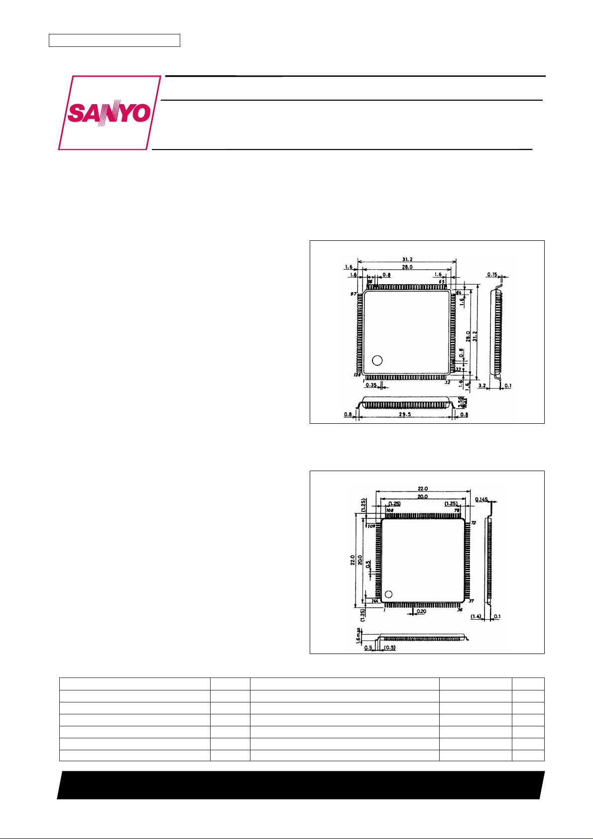
Package Dimensions
unit: mm
3182-QIP128E
unit: mm
3214-SQFP144
Preliminary
SANYO: QIP128E
[LC895125Q]
SANYO: SQFP144
[LC895125W]
LC895125Q, 895125W
SANYO Electric Co.,Ltd. Semiconductor Bussiness Headquarters
TOKYO OFFICE Tokyo Bldg., 1-10, 1 Chome, Ueno, Taito-ku, TOKYO, 110-0005 JAPAN
CD-ROM Driver with On-Chip SCSI Interface and
Subcode Functions
CMOS LSI
Specifications
Absolute Maximum Ratings at VSS= 0 V
Parameter Symbol Conditions Ratings Unit
Maximum supply voltage V
DD
max Ta = 25°C –0.3 to +7.0 V
I/O voltages V
I
, V
O
Ta = 25°C –0.3 to VDD+ 0.3 V
Allowable power dissipation Pd max Ta ≤ 70°C 450 mW
Operating temperature Topr –30 to +70 °C
Storage temperature Tstg –55 to +125 °C
Soldering heat resistance (pins only) 10 seconds 260 °C
Page 2
Allowable Operating Ranges at Ta = –30 to +70°C, VSS= 0 V
DC Characteristics at VSS= 0 V, VDD= 4.5 to 5.5 V, Ta = –30 to +70°C
SCSI Pin Input Characteristics
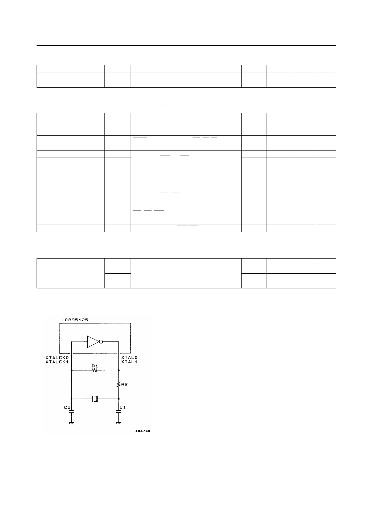
Sample Recommended Oscillator Circuit
R1 = 120 kΩ
R2 = 47 Ω
C1 = 30 pF
Crystal oscillator frequencies: XTALCK0 = 16.9344 MH
Z and XTALCK1 = 20 MHz
or:
R1 = 3.3 kΩ
R2 = None
C1 = 5 pF
Crystal oscillator frequency: XTALCK0 = 33.8688 MHz
If third harmonic overtones appear when using a 33.8688 MHz frequency with the
recommended circuit example, consult with the manufacturer of the crystal
element, since detailed values of the circuit constants will be influenced by the
printed circuit board.
No. 5241-2/11
LC895125Q, 895125W
Parameter Symbol Applicable Pins* (See below) min typ max Unit
Input high level voltage V
IH
1
All input pins other than (1), (3), and XTALCK
2.2 V
Input low level voltage V
IL
1 0.8 V
Input high level voltage V
IH
2
RESET, IO0 to IO15, D0 to D7, RD, CS, WR, WFCK,
2.5 V
Input low level voltage V
IL
2
SBSO, SCOR (1)
0.6 V
Input high level voltage V
IH
3
Input pins (3), ACK, and ATN
2.0 V
Input low level voltage V
IL
3 0.8 V
Output high level voltage V
OH
1
I
OH
1 = –2 mA: All output pins except (2), (3),
2.4 V
and XTALCK, IO0 to IO15, and D0 to D7
Output low level voltage V
OL
1
I
OL
1 = 2 mA: All output pins except (2), (3),
0.4 V
and XTALCK, IO0 to IO15, and D0 to D7
Output low level voltage V
OL
2
I
OL
2 = 2 mA: INT1, INT0, and ZSWAIT
0.4 V
(open-drain outputs with pull-up resistors) (2)
Output low level voltage V
OL
3
I
OL
3 = 48 mA: DB0, to DB7, DBP, BSY, I/O, MSG,
0.4 V
SEL, RST, REQ, C/D (3)
Input leakage current I
L
VI= VSS, VDD: All input pins –25 +25 µA
Pull-up resistance R
UP
IO0 to IO15, D0 to D7, INT0, INT1, ZSWAIT 40 80 160 kΩ
Parameter Symbol Conditions min typ max Unit
Supply voltage V
DD
4.5 5.0 5.5 V
Input voltage range V
IN
0 V
DD
V
Parameter Symbol Conditions min typ max Unit
Input threshold voltage
V
t + t1
VDD= 4.5 to 5.5 V
1.60 2.00 V
V
t – t1
0.80 1.11 V
Hysteresis width ∆V
tt1
VDD= 5.0 V 0.41 0.49 V
Page 3
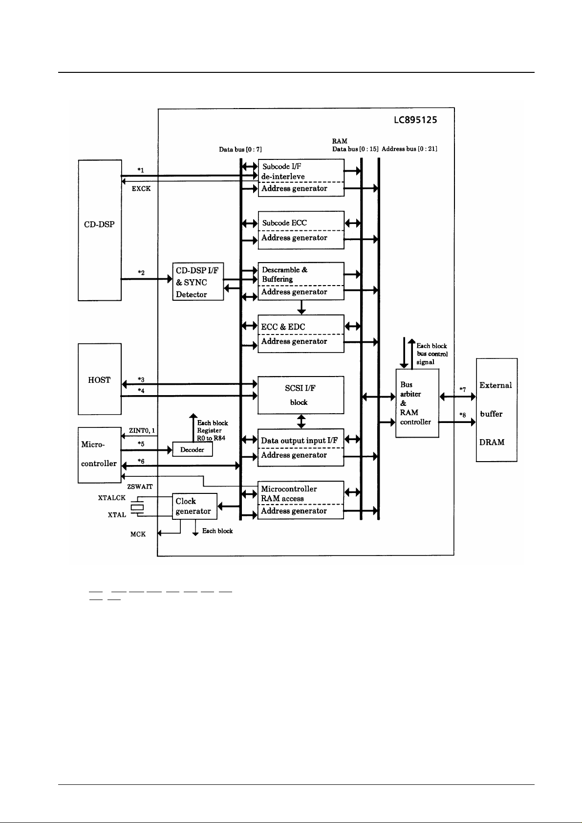
Block Diagram
Note: 1. WFCK, SBSO, SCOR
2. BCK, SDATA, LRCK, C2PO
3. DB0 to DB7, DBP, BSY, MSG, SEL, RST, REQ, I/O, C/D
4. ACK, ATN
5. ZRD, ZWR, SUA0 to SUA6, ZCS, CSCTRL
6. D0 to D7
7. IO0 to IO15
8. RA0 to RA16, ZRAS0, ZRAS1, ZCAS0, ZCAS1, ZOE, ZUWE, ZLWE
Note: IO8 to IO15 and RA9 to RA16 are the same pins.
No. 5241-3/11
LC895125Q, 895125W
Page 4
Pin Functions (LC895125Q)
Type: I: Input pin, O: Output pin, B: Bidirectional pin, P: Power supply pin, NC: No connection pin
Note: 1. NC pins must be left open. Do not connect any signal to these pins.
2. Pin names that start with Z are negative-logic signals.
3. V
SS0
is the logic system ground and V
SS1
is the SCSI interface ground.
4. Applications that use DRAM must insert resistors in the CAS and RAS lines, connect capacitors between these lines and ground, and take any
other measures necessary to prevent undershoot in the DRAM related circuits.
5. Since these circuits include buffers that sink 48 mA, adequate noise prevention measures must be applied.
No. 5241-4/11
LC895125Q, 895125W
Pin No. Symbol Type Function
1 V
DD
P
2 V
SS0
P
3 RA5 O
4 RA6 O
Address outputs for the buffer RAM
5 RA7 O
6 RA8 O
7 RA9 (IO15) B
Address outputs for the buffer RAM or data I/O pins
8 RA10 (IO14) B
The pin circuits include pull-up resistors.
9 V
SS0
P
10 RA11 (IO13) B
11 RA12 (IO12) B
12 RA13 (IO11) B
Address outputs for the buffer RAM or data I/O pins
13 RA14 (IO10) B
The pin circuits include pull-up resistors.
14 RA15 (IO9) B
15 RA16 (IO8) B
16 IO7 B Buffer RAM data I/O. The pin circuit includes a pull-up resistor.
17 V
SS0
P
18 IO6 B
19 IO5 B
20 IO4 B
Buffer RAM data I/O.
21 IO3 B
The pin circuits include pull-up resistors.
22 IO2 B
23 IO1 B
24 IO0 B
25 V
SS0
P
26 TEST0 I
27 TEST1 I
28 TEST2 I Test pins. These pins must be connected to V
SS0
.
29 TEST3 I
30 TEST4 I
31 ZRESET I LSI reset. The LSI is reset on a 0 input.
32 V
DD
P
33 V
SS0
P
34 CSCTRL I Selects active-high or active-low for the microcontroller CS logic.
35 XTALCK0 I Crystal oscillator input
36 XTAL0 O Crystal oscillator output
37 V
SS0
P
38 D0 B
39 D1 B
40 D2 B
41 D3 B
Microcontroller data signals
42 D4 B
43 D5 B
44 D6 B
45 D7 B
46 V
SS0
P
47 ZSWAIT O WAIT signal output to the microcontroller
48 ZINT0 O Interrupt request output to the microcontroller (ECC side. Set with a register.)
49 V
DD
P
50 ZINT1 O Interrupt request output to the microcontroller (SCSI side. Set with a register.)
Continued on next page.
Page 5

Continued from preceding page.
Type: I: Input pin, O: Output pin, B: Bidirectional pin, P: Power supply pin, NC: No connection pin
Note: 1. NC pins must be left open. Do not connect any signal to these pins.
2. Pin names that start with Z are negative-logic signals.
3. V
SS0
is the logic system ground and V
SS1
is the SCSI interface ground.
4. Applications that use DRAM must insert resistors in the CAS and RAS lines, connect capacitors between these lines and ground, and take any
other measures necessary to prevent undershoot in the DRAM related circuits.
5. Since these circuits include buffers that sink 48 mA, adequate noise prevention measures must be applied.
No. 5241-5/11
LC895125Q, 895125W
Pin No. Symbol Type Function
51 ZRD I Microcontroller data read signal input
52 ZWR I Microcontroller data write signal input
53 ZCS I Register chip select signal from the microcontroller
54 SUA0 I
55 SUA1 I
56 SUA2 I
57 SUA3 I Microcontroller register selection signals
58 SUA4 I
59 SUA5 I
60 SUA6 I
61 V
SS0
P
62 X1EN I Selection pin that must be set to 1 when XTALCK1 is used.
63 XTALCK1 I SCSI block oscillator circuit input. Selected by X1EN.
64 XTAL1 O SCSI block oscillator circuit output.
65 V
DD
P
66 V
SS1
P
67 DB0 B
SCSI connection
68 DB1 B
69 V
SS1
P
70 DB2 B
SCSI connection
71 DB3 B
72 V
DD
P
73 V
SS1
P
74 DB4 B
SCSI connection
75 DB5 B
76 V
SS1
P
77 DB6 B
SCSI connection
78 DB7 B
79 V
SS1
P
80 DBP B SCSI connection
81 V
SS1
P
82 ATN B SCSI connection
83 V
DD
P
84 BSY B
SCSI connection
85 ACK B
86 V
SS1
P
87 RST B
SCSI connection
88 MSG B
89 V
DD
P
90 SEL B
SCSI connection
91 C/D B
92 V
SS1
P
93 REQ B
SCSI connection
94 I/O B
95 V
SS1
P
96 V
DD
P
97 V
SS0
P
98 NC
99 V
SS0
P
100 V
SS0
P
Continued on next page.
Page 6

Continued from preceding page.
Type: I: Input pin, O: Output pin, B: Bidirectional pin, P: Power supply pin, NC: No connection pin
Note: 1. NC pins must be left open. Do not connect any signal to these pins.
2. Pin names that start with Z are negative-logic signals.
3. V
SS0
is the logic system ground and V
SS1
is the SCSI interface ground.
4. Applications that use DRAM must insert resistors in the CAS and RAS lines, connect capacitors between these lines and ground, and take any
other measures necessary to prevent undershoot in the DRAM related circuits.
5. Since these circuits include buffers that sink 48 mA, adequate noise prevention measures must be applied.
No. 5241-6/11
LC895125Q, 895125W
Pin No. Symbol Type Function
101 V
SS0
P
102 NC
103 NC
104 C2PO I
105 SDATA I
CD DSP interface
106 BCK I
107 LRCK I
108 MCK O Outputs the XTALCK0 frequency, or that frequency divided by 2.
109 V
SS0
P
110 EXCK O
111 WFCK I Subcode I/O
112 SBSO I
113 V
DD
P
114 SCOR I Subcode I/O
115 V
SS0
P
116 ZRAS0 O Buffer RAM RAS signal output pin 0 (Normally, pin 0 is used)
117 ZRAS1 O Buffer RAM RAS signal output pin 1
118 ZCAS0 O Buffer RAM CAS signal output pin 0 (Normally, pin 0 is used)
119 ZCAS1 O Buffer RAM CAS signal output pin 1
120 ZOE O Buffer RAM output enable
121 ZUWE O Buffer RAM upper write enable
122 ZLWE O Buffer RAM lower write enable
123 V
SS0
P
124 RA0 O
125 RA1 O
126 RA2 O Buffer RAM address signal outputs
127 RA3 O
128 RA4 O
Page 7

Pin Functions (LC895125W)
Type: I: Input pin, O: Output pin, B: Bidirectional pin, P: Power supply pin, NC: No connection pin
Note: 1. NC pins must be left open. Do not connect any signal to these pins.
2. Pin names that start with Z are negative-logic signals.
3. V
SS0
is the logic system ground and V
SS1
is the SCSI interface ground.
4. Applications that use DRAM must insert resistors in the CAS and RAS lines, connect capacitors between these lines and ground, and take any
other measures necessary to prevent undershoot in the DRAM related circuits.
5. Since these circuits include buffers that sink 48 mA, adequate noise prevention measures must be applied.
No. 5241-7/11
LC895125Q, 895125W
Pin No. Symbol Type Function
1 V
SS0
P
2 V
DD
P
3 V
SS0
P
4 RA5 O
5 RA6 O
Buffer RAM address signal outputs
6 RA7 O
7 RA8 O
8 RA9 (IO15) B
Address outputs for the buffer RAM or data I/O pins
9 RA10 (IO14) B
The pin circuits include pull-up resistors.
10 V
SS0
P
11 RA11 (IO13) B
12 RA12 (IO12) B
13 RA13 (IO11) B
Address outputs for the buffer RAM or data I/O pins
14 RA14 (IO10) B
The pin circuits include pull-up resistors.
15 RA15 (IO9) B
16 RA16 (IO8) B
17 IO7 B Buffer RAM data I/O. The pin circuit includes a pull-up resistor.
18 V
DD
P
19 V
SS0
P
20 NC
21 IO6 B
22 IO5 B
23 IO4 B
Buffer RAM data I/O.
24 IO3 B
The pin circuit includes a pull-up resistor.
25 IO2 B
26 IO1 B
27 IO0 B
28 V
SS0
P
29 TEST0 I
30 TEST1 I
31 TEST2 I Test pins. These pins must be connected to V
SS0
.
32 TEST3 I
33 TEST4 I
34 ZRESET I LSI reset. The LSI is reset on a 0 input.
35 V
DD
P
36 V
SS0
P
37 V
DD
P
38 V
SS0
P
39 CSCTRL I Selects active-high or active-low for the microcontroller CS logic.
40 XTALCK0 I Crystal oscillator input
41 XTAL0 O Crystal oscillator output
42 V
SS0
P
43 D0 B
44 D1 B
45 D2 B
46 D3 B
Microcontroller data signals
47 D4 B
48 D5 B
49 D6 B
50 D7 B
Continued on next page.
Page 8

Continued from preceding page.
Type: I: Input pin, O: Output pin, B: Bidirectional pin, P: Power supply pin, NC: No connection pin
Note: 1. NC pins must be left open. Do not connect any signal to these pins.
2. Pin names that start with Z are negative-logic signals.
3. V
SS0
is the logic system ground and V
SS1
is the SCSI interface ground.
4. Applications that use DRAM must insert resistors in the CAS and RAS lines, connect capacitors between these lines and ground, and take any
other measures necessary to prevent undershoot in the DRAM related circuits.
5. Since these circuits include buffers that sink 48 mA, adequate noise prevention measures must be applied.
No. 5241-8/11
LC895125Q, 895125W
Pin No. Symbol Type Function
51 V
SS0
P
52 ZSWAIT O WAIT signal output to the microcontroller
53 ZINT0 O Interrupt request output to the microcontroller (ECC side. Set with a register.)
54 V
DD
P
55 V
SS0
P
56 ZINT1 O Interrupt request output to the microcontroller (SCSI side. Set with a register.)
57 ZRD I Microcontroller data read signal input
58 NC
59 ZWR I Microcontroller data write signal input
60 ZCS I Input for the register chip select signal from the microcontroller
61 SUA0 I
62 SUA1 I
63 SUA2 I
64 SUA3 I Microcontroller register selection signals
65 SUA4 I
66 SUA5 I
67 SUA6 I
68 V
SS0
P
69 X1EN I Selection pin that must be set to 1 when XTALCK1 is used
70 XTALCK1 I SCSI block oscillator circuit input. Selected by X1EN.
71 XTAL1 O SCSI block oscillator circuit output
72 V
SS0
P
73 V
DD
P
74 V
SS1
P
75 DB0 B
SCSI connection
76 DB1 B
77 V
SS1
P
78 DB2 B
SCSI connection
79 DB3 B
80 NC
81 V
DD
P
82 V
SS1
P
83 DB4 B
SCSI connection
84 DB5 B
85 V
SS1
P
86 DB6 B
SCSI connection
87 DB7 B
88 V
SS1
P
89 DBP B SCSI connection
90 V
DD
P
91 V
SS1
P
92 NC
93 ATN B SCSI connection
94 V
DD
P
95 BSY B
SCSI connection
96 ACK B
97 V
SS1
P
98 RST B
SCSI connection
99 MSG B
100 V
DD
P
Continued on next page.
Page 9

Continued from preceding page.
Type: I: Input pin, O: Output pin, B: Bidirectional pin, P: Power supply pin, NC: No connection pin
Note: 1. NC pins must be left open. Do not connect any signal to these pins.
2. Pin names that start with Z are negative-logic signals.
3. V
SS0
is the logic system ground and V
SS1
is the SCSI interface ground.
4. Applications that use DRAM must insert resistors in the CAS and RAS lines, connect capacitors between these lines and ground, and take any
other measures necessary to prevent undershoot in the DRAM related circuits.
5. Since these circuits include buffers that sink 48 mA, adequate noise prevention measures must be applied.
No. 5241-9/11
LC895125Q, 895125W
Pin No. Symbol Type Function
101 SEL B
SCSI connection
102 C/D B
103 V
SS1
P
104 REQ B
SCSI connection
105 I/O B
106 V
SS1
P
107 V
DD
P
108 V
SS0
P
109 V
DD
P
110 V
SS0
P
111 NC
112 V
SS0
P
113 V
SS0
P
114 V
SS0
P
115 NC
116 NC
117 C2PO I
118 SDATA I
CD DSP interface
119 BCK I
120 LRCK I
121 MCK O Outputs the XTALCK0 frequency, or that frequency divided by 2.
122 V
SS0
P
123 EXCK O
124 WFCK I Subcode I/O
125 SBSO I
126 V
DD
P
127 V
SS0
P
128 SCOR I Subcode I/O
129 V
SS0
P
130 NC
131 ZRAS0 O Buffer RAM RAS signal output pin 0 (Normally, pin 0 is used)
132 ZRAS1 O Buffer RAM RAS signal output pin 1
133 ZCAS0 O Buffer RAM CAS signal output pin 0 (Normally, pin 0 is used)
134 ZCAS1 O Buffer RAM CAS signal output pin 1
135 ZOE O Buffer RAM output enable
136 ZUWE O Buffer RAM upper write enable
137 ZLWE O Buffer RAM lower write enable
138 V
SS0
P
139 RA0 O
140 RA1 O
141 RA2 O Buffer RAM address signal outputs
142 RA3 O
143 RA4 O
144 V
DD
P
Page 10

Pin Functions
1. SCSI Pins
• BSY, ACK, MSG, SEL, REQ, ATN, I/O, C/D (input and output)
SCSI bus control pins.
• DB0 to DB7, DBPB (input and output)
These are the SCSI data bus pins.
2. Microcontroller Interface Pins
• ZCS (input)
Microcontroller chip select line
• CSCTRL (input)
Microcontroller chip select logic selection signal
High - ZCS is an active low signal.
Low - ZCS is an active high signal.
• ZRD, ZWR, SUA0 to SUA6 (input)
Microcontroller interface control signal
The SUA0 to SUA6 pins are used for addressing.
• ZSWAIT (output)
When the microcontroller accesses RAM, it must wait if this pin is low.
This is a built-in pull-up resistor open-drain output.
• D7 to D0 (input and output)
Microcontroller data bus. Pull-up resistors are built in.
• ZINT0, ZINT1 (output)
Interrupt request output to the microcontroller. A SCSI-side interrupt can be output from ZINT1 by setting the C
register (bit 7 in R11).
This is a built-in pull-up resistor open-drain output.
3. Buffer RAM Pins
• IO0 to IO15 (input and output)
Buffer RAM data bus. Pull-up resistors are built in. The IO8 to IO15 pins have shared functions as the RA9 to
RA16 pins.
This means that 16-bit PSRAM cannot be used.
• RA0 to RA16 (output)
Buffer RAM address lines. RA9 to RA16 have shared functions as the IO8 to IO15 pins.
This means that 16-bit PSRAM cannot be used.
• ZRAS0, ZRAS1, (ZCS0), (ZCS1) (output)
Buffer DRAM RAS outputs. Normally, ZRAS0 is used. However, when two 1-MB (64k × 16-bit) DRAM chips
are used, the respective DRAM RAS pins are connected to ZRAS0 and ZRAS1. Connected to the CS pin if
PSRAM is used.
• ZCAS0, ZCAS1 (output)
Buffer DRAM CAS outputs. Normally, ZCAS0 is used. However, when two 1-MB (64k × 16-bit) DRAM chips
are used, the respective DRAM CAS pins are connected to ZCAS0.
• ZOE (output)
Buffer RAM read output signal
• ZUWE, ZLWE (output)
Buffer RAM write output signals. Connected to the corresponding pins on the RAM chip.
Leave ZUWE open if an 8-bit RAM is used.
4. Subcode Interface Pins
• EXCK, WFCK, SBSO, SCOR (input and output)
Subcode interface pins. Connecting a CD DSP using these pins allows the LC895125 to read in subcode data and
transfer it to the host.
No. 5241-10/11
LC895125Q, 895125W
Page 11

PS No. 5241-11/11
LC895125Q, 895125W
This catalog provides information as of February, 1996. Specifications and information herein are subject to
change without notice.
■ No products described or contained herein are intended for use in surgical implants, life-support systems, aerospace
equipment, nuclear power control systems, vehicles, disaster/crime-prevention equipment and the like, the failure of
which may directly or indirectly cause injury, death or property loss.
■ Anyone purchasing any products described or contained herein for an above-mentioned use shall:
➀ Accept full responsibility and indemnify and defend SANYO ELECTRIC CO., LTD., its affiliates, subsidiaries and
distributors and all their officers and employees, jointly and severally, against any and all claims and litigation and all
damages, cost and expenses associated with such use:
➁ Not impose any responsibility for any fault or negligence which may be cited in any such claim or litigation on
SANYO ELECTRIC CO., LTD., its affiliates, subsidiaries and distributors or any of their officers and employees
jointly or severally.
■ Information (including circuit diagrams and circuit parameters) herein is for example only; it is not guaranteed for
volume production. SANYO believes information herein is accurate and reliable, but no guarantees are made or implied
regarding its use or any infringements of intellectual property rights or other rights of third parties.
5. CD DSP Data Pins
• BCK, SDATA, LRCK, C2PO (input)
The LC895125 reads in CD-ROM data over these pins connected to a CD DSP.
C2PO is the C2 flag pin.
6. Other Pins
• ZRESET (input)
Reset input to the LC895125. The LC895125 is reset by a low-level input.
This pin must be held low for a period of at least 1 µs when power is first applied.
• XTALCK0, XTAL0
The main clock for the ECC and SCSI blocks. These pins support frequencies from 16.9344 to 25 MHz.
When a double-frequency input is used, these pins accept frequencies up to 38 MHz.
Use a double-frequency input when a ceramic oscillator and DRAM are used.
(This is because the internal clock must have a 50% duty.)
An external clock may input to the XTALCK pin.
The SCSI block main clock can also be provided from XTALCK1 and XTAL1 if so specified by the setting of
X1EN (pin 89).
• XTALCK1, XTAL1
The main clock for the ECC and SCSI blocks. These pins are enabled for oscillator operation by setting X1EN (pin
89). The LC895125 is designed so that the ECC and SCSI blocks can also be operated asynchronously.
This means that precise 10-MB/s synchronous transfers can be achieved by providing a 20-MHz input to
XTALCK1 and XTAL1.
A ceramic oscillator may be used here since only the rising edge of this signal is used.
In applications that do not use these pins, XTALCK1 must be tied to V
SS
and XTAL1 must be left open.
• X1EN (input)
Set this pin to 1 to us use XTALCK1 and XTAL1 for the SCSI block main clock.
Set this pin to 0 to drive both the ECC and SCSI blocks from XTALCK0 and XTAL0.
• MCK (output)
Outputs either the XTALCK0 frequency or that frequency divided by 2. This pin’s output can also be stopped if
desired.
 Loading...