

Page 1
Ordering number : ENN*6844
LC863532A/28A/24A/20A/16A
8-Bit Single-Chip Microcontroller
Preliminary
Overview
The LC863532/28/24/20/16A are 8-bit single chip microcontrollers with the following on-chip functional blocks:
- CPU : Operable at a minimum bus cycle time of 0.424µs
- On-chip R O M capaci ty
Program ROM : 32K/28K/24K/20K/16K bytes
CGROM : 16K bytes
- On-chip RAM capacity : 512 bytes
- OSD RAM : 352 × 9 bits
- Closed-Caption TV controller and the on-screen display controller
- Four channels × 6-bit AD Converter
- Three channels × 7-bit PWM
- Two channels × 16-bit timer/counter, 14-bit base timer
- IIC-bus compliant serial interface circuit (Multi-master type)
- ROM correction function
- 12-source 8-vectored interrupt system
- Integrated system clock generator and display clock generator
Only one X’tal oscillator (32.768kHz) for PLL reference is used for both generators
TV control and the Closed Caption function
All of the above functions are fabricated on a single chip.
Note : This product includes the IIC bus interface circuit. If you intend to use the IIC bus interface, please
notify us of this in advance of our receiving your program ROM code order.
Purchase of SANYO IIC components conveys a license under the Philips IIC Patents Rights to use these
components in an IIC system, provided that the system conforms to the IIC Standard Specification as
defined by Philips.
Trademarks
II C is a trademark of Philips Corporation.
CMOS IC
Ver.1.00
00000
D2700 RM (IM) Shindo No.6844-1/19
Page 2
LC863532A/28A/24A/20A/16A
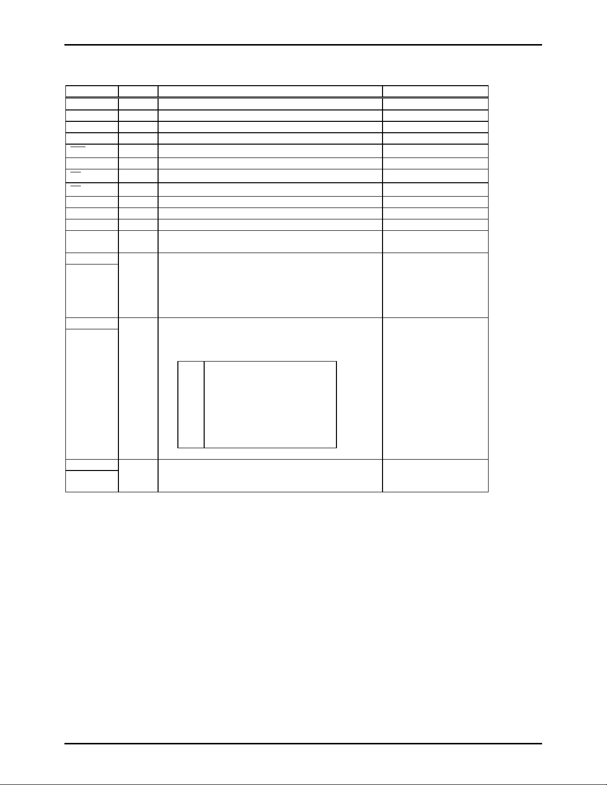
Features
(1) Read-Only Memory (ROM) : 32768 × 8 bits / 28672 × 8 bits / 24576 × 8 bits
20486 × 8 bits / 16384 × 8 bits for program
16128
(2) Random Access Memory (RAM) : 384 × 8 bits (working area)
128
352
(3) OSD functions
- Screen display : 36 characters × 16 lines (by software)
- RAM : 352 words (9 bits per word)
Display area : 36 words × 8 lines
Control area : 8 words × 8 lines
- Characters
Up to 252 kinds of 16 × 32 dot character fonts
(4 characters including 1 test character are not programmable)
Each font can be divided into two parts and used as two fonts (Ex. 16 × 16 dot character font × 2)
At least 111 characters need to be divide between a 16×18 dot and 8 × 9 dot character font to display the caption
fonts.
- Various character attributes
Character colors : 16 colors (analog mode: lv
Character background colors : 16 colors (analog mode: lv
Fringe / shadow colors : 16 colo rs (analog mode: lv
Full screen colors : 16 colors (analog mode: lv
Rounding
Underline
Italic character (slanting)
- Attribute can be changed without spacing
- Vertical display start line number can be set for each row independently (Rows can be overlapped)
- Horizontal display start position can be set for each row independently
- Horizontal pitch (bit 9 - 16)
*1
and vertical pitch (bit-32) can be set for each row independently
- Different display modes can be set for each row independentl y
Caption • Text mode / OSD mode 1 / OSD mode 2 (Quarter size) / Simplifed graphic mode
- Ten character sizes
*1
Horez. × Vert. = (1 × 1), (1 × 2), (2 × 2), (2 × 4), (0.5 × 0.5)
(1.5 × 1), (1.5 × 2), (3 × 2), (3 × 4), (0.75 × 0.5)
- Shuttering and scrolling on each row
- Simplified Graphic Display
*1 Note : ran ge depends on display mode : r efer to the manual f o r details.
(4) Bus Cycle Time / Instruction-Cycle Time
Bus cycle time Instruction cycle time Clock divider System clock oscillation Oscillation Frequency Voltage
0.424µs 0.848µs
7.5µs 15.0µs
91.55µs 183.1µs
183.1µs 366.2µs
1/2 Internal VCO
1/2 Internal RC 800kHz 4.5V to 5.5V
1/1 Crystal 32.768kHz 4.5V to 5.5V
1/2 Crystal 32.768kHz 4.5V to 5.5V
(5) Ports
- Input / Output Ports : 4 ports (24 terminals)
Data direction programmable in nibble units : 1 port (8 terminals)
(If the N-ch open drain output is selected by option, the corresponding port data can be read in output mode.)
Data direction programmable for each bit individually : 3 ports (1 6 terminals)
8 bits for CGROM
×
8 bits (working or ROM correction function)
×
9 bits (for CRT display)
×
output) / 8 colors (digital/mode)
p-p
output) / 8 colors (digital/mode)
p-p
output) / 8 colors (digital/mode)
p-p
output) / 8 colors (digital/mode)
p-p
14.156MHz 4.5V to 5.5V
(Ref : X’tal 32.768kHz)
No.6844-2/19
Page 3

LC863532A/28A/24A/20A/16A
(6) AD converter
- 4 channels × 6-bit AD converters
(7) Serial interfaces
- IIC-bus compliant serial interface (Multi-master type)
Consists of a single built-in circuit with two I/O channels. The two data lines and two clock lines can be connected
internally.
(8) PWM output
- 3 channels × 7-bit PWM
(9) Timer
- Timer 0 : 16-bit timer/counter
With 2-bit prescaler + 8-bit programmable prescaler
Mode 0 : Two 8- bit tim e rs with a progra mmabl e prescale r
Mode 1 : 8-bit timer with a programmable prescaler + 8-bit counter
Mode 2 : 16-bit timer with a programmable prescaler
Mode 3 : 16-bit counter
The resolution o f ti mer is 1 tCYC.
- Timer 1 : 16-bit timer/PWM
Mode 0 : Two 8- bit time rs
Mode 1 : 8-bit timer + 8-bit PWM
Mode 2 : 16-bit timer
Mode 3 : a variable-bit PWM (9 to 16 bits)
In mode 0/1, the resolution of timer/PWM is 1 tCYC
In mode 2/3, the resolution of timer/PWM is selectable by program; tCYC or 1/2 tCYC
- Base timer
Generate every 500ms overflow for a clock application (using 32.768kHz crystal oscillation for the base timer clock)
Generate every 976µs, 3.9ms, 15.6ms, 62.5ms overflow (using 32.768kHz crystal oscillation for the base timer
clock)
Clock for the base timer is selectable from 32.768kHz crystal oscillation, system clock or programmable prescaler
output of Timer 0
(10) Remote control receiver circuit (connected to the P73/INT3/T0IN terminal)
- Noise rejection function
- Polarity switching
(11) Watchdog timer
External RC circuit is required
Interrupt or system reset is activated when the timer overflows
(12) ROM correction function
Max 128 bytes / 2 addresses
No.6844-3/19
Page 4

LC863532A/28A/24A/20A/16A
(13) Interrupts
- 12 sources 8 vectored interrupts
1. External Interrupt INT0
2. External Interrupt INT1
3. External Interrupt INT2, Timer/counter T0L (Lower 8 bits)
4. External Interrupt INT3, base timer
5. Timer/counter T0H (Upper 8 bits)
6. Timer T1H, Timer T1L
7. Vertical synchronous signal interrupt (
), horizontal line (
VS
HS
)
8. IIC
- Interrupt prior ity control
Three interrupt priorities are supported (low, high and highest) and multi-level nesting is possible. Low or high
priority can be assigned to the interrupts from 3 to 8 listed above. For the external interrupt INT0 and INT1, low or
highest priority can be set.
(14) Sub-routine stack level
- A maximum of 128 levels (stack is b uilt in the inter n al RAM)
(15) Multiplication/division instruction
- 16 bits × 8 bits (7 instruction cycle times)
- 16 bits / 8 bits (7 instruction cycle times)
(16) 3 oscillation circuits
- Built-in RC oscillation circuit used for the system clock
- Built-in VCO circuit used for the system clock and OSD
- X’tal oscillation circuit used for base timer, system clock and PLL reference
(17) Standby function
- HALT mode
The HALT mode is used to reduce the power dissipation. In this operation mode, the program execution is
stopped. This mode can be released by the interrupt request or the system reset.
- HOLD mode
The HOLD mode is used to stop the oscillations; RC (internal), VCO, and X’tal oscillations. This mode can be
released by the following conditions.
Pull the reset terminal (
•
Feed the selected level to either P70/INT0 or P71/INT1.
•
) to low level.
RES
(18) Package
- MFP36S
- DIP36S
(19) Development tools
- Flash EEPROM: LC86 F3548A
- Evaluation chip: LC863096
- Emulator: EVA86000 (main) + ECB863400 (evaluation chip board)
+ POD36-CABLE (cable)
+ POD36-DIP (for DIP36S)
or POD36-MFP (for MFP36S)
No.6844-4/19
Page 5
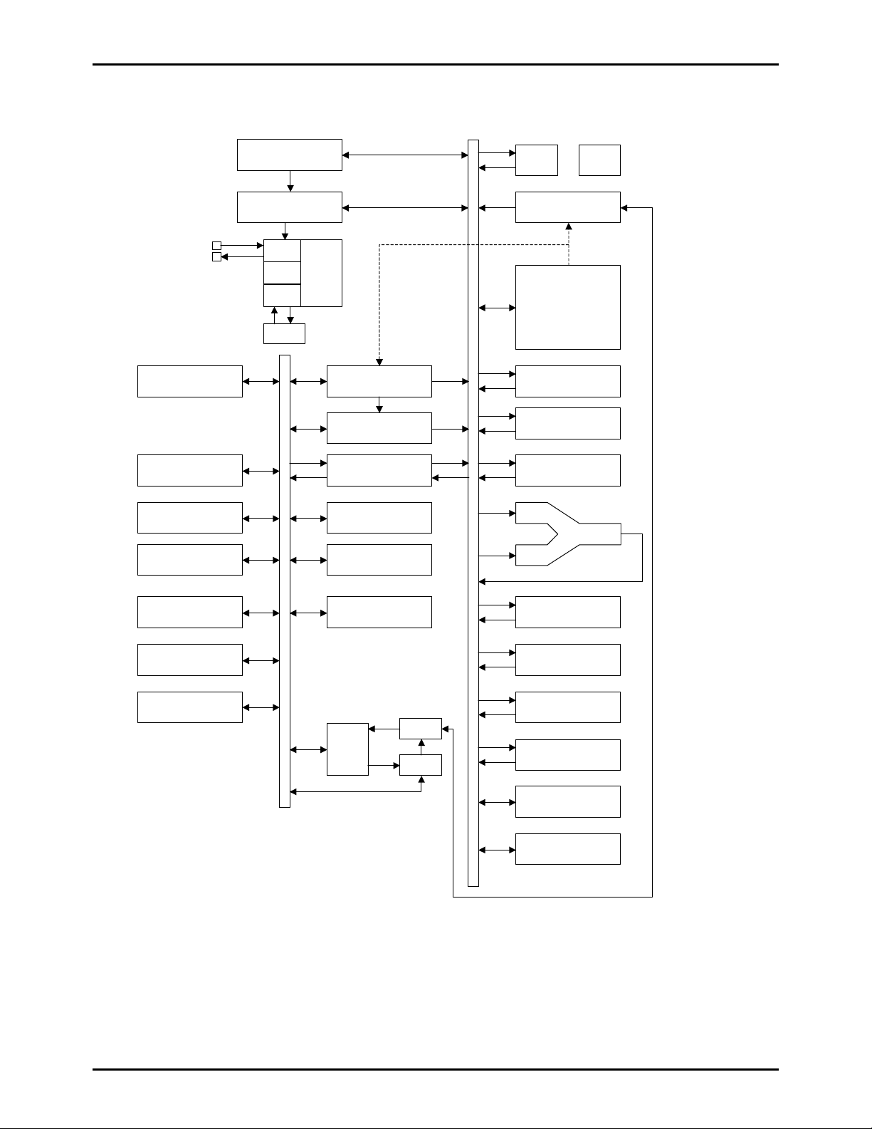
System Bl ock Diagram
IIC
Timer 0
Timer 1
Base Timer
ADC
INT0-3
Noise Rejection Filter
PWM
Interrupt Control
Standby Control
X’tal
RC
VCO
PLL
LC863532A/28A/24A/20A/16A
Clock
Generator
ROM Correct Control
XRAM
Bus Interface
Port 1
Port 3
Port 7
OSD
Control
Circuit
CGROM
VRAM
IR PLA
ROM
PC
ACC
B Register
C Register
ALU
PSW
RAR
RAM
Stack Pointer
Port 0
Watch Dog Timer
No.6844-5/19
Page 6
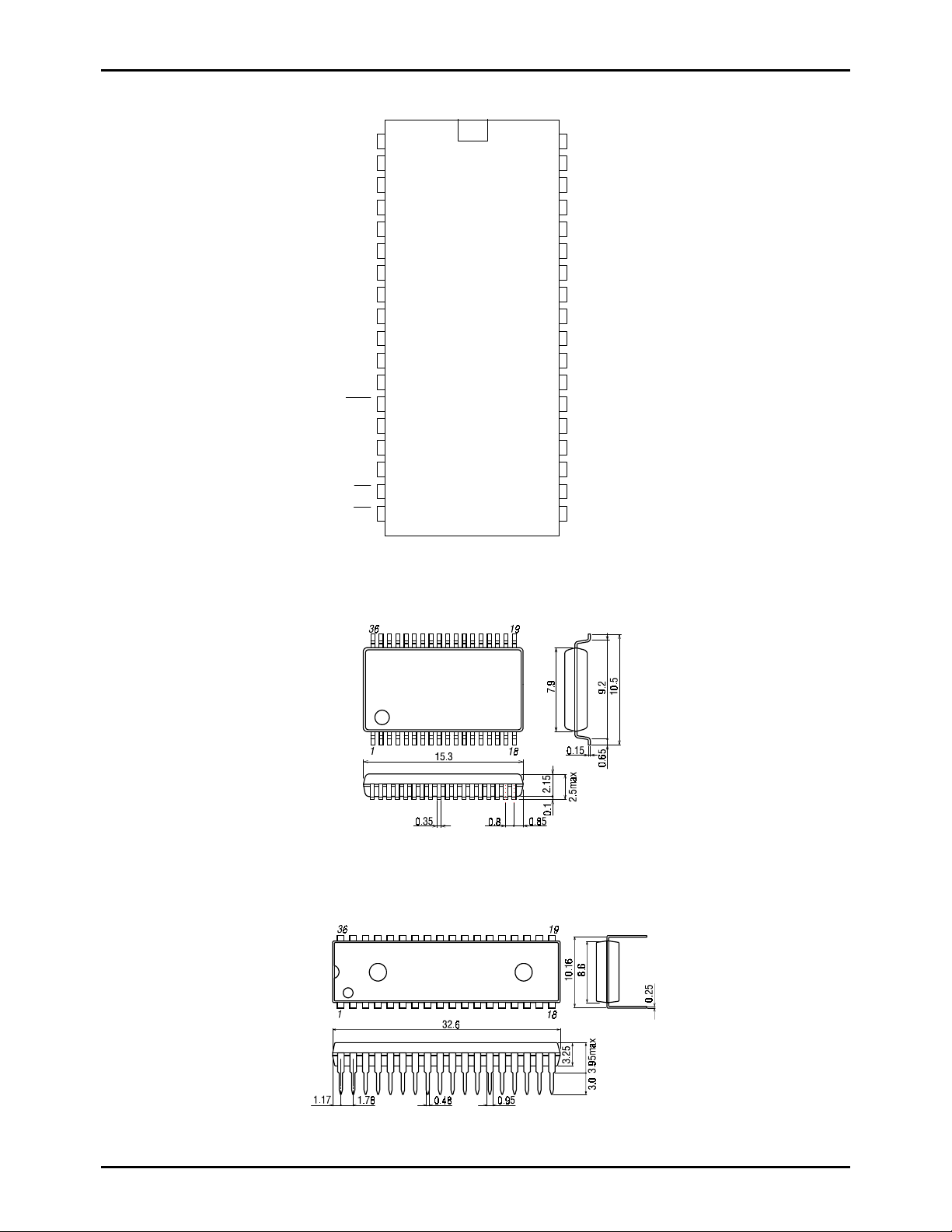
Pin Assignment
Package Dimension
(unit : mm)
3204
Package Dimension
(unit : mm)
3170
P10/SDA0
P11/SCLK0
P12/SDA1
P13/SCLK1
VSS
XT1
XT2
VDD
P04/AN4
P05/AN5
P06/AN6
P07/AN7
RES
FILT
P33
P30
VS
HS
LC863532A/28A/24A/20A/16A
1
2
3
4
5
6
7
8
9
10
11
12
13
14
15
16
17
18
36
35
34
33
32
31
30
29
28
27
26
25
24
23
22
21
20
19
P03
P02
P01
P00
P17
P16/PWM3
P15/PWM2
P14/PWM1
P73/INT3/T0IN
P72/INT2/T0IN
P71/INT1
P70/INT0
P32
P31
BL
B
G
R
SANYO : MFP-36S
SANYO : DIP-36S
No.6844-6/19
Page 7
LC863532A/28A/24A/20A/16A
Pin Description
Pin Description Table
Terminal I/O Function Description Option
VSS - Negative power supply
XT1 I Input terminal for crystal oscillator
XT2 O Output terminal for crystal oscillator
VDD - Positive power supply
RES
FILT O Filter terminal for PLL
VS
HS
R O Red (R) output terminal of RGB image output
G O Green (G) output terminal of RGB image output
B O Blue (B) output terminal of RGB image output
BL O Fast blanking control signal
Port 0
P00 to P07
Port 1 •8-bit input/output port
P10 to P17
Port 3
P30 to P33
I Reset terminal
I Vertical synchronization signal input terminal
I Horizontal synchronization signal input terminal
Switch TV image signal and captio n/OSD image signal
I/O
I/O
I/O
•8-bit input/output port,
Input/output can be specified in nibble unit
(If the N-ch open drain output is selected by option, the
corresponding port data can be read in output mode.)
•Other functions
AD converter input port (P04 to P07: 4 channels)
Input/output can be specified for each bit
(programmable pull-up resister provided)
•Other functions
P10
•4-bit input/output port
Input/output can be specified for each bit
(CMOS output/input with programmable pull-up resister)
IIC0 data I/O
P11
IIC0 clock output
P12
IIC1 data I/O
P13
IIC1 clock output
P14
PWM1 output
P15
PWM2 output
P16
PWM3 output
P17
Timer 1 (PWM) outp ut
Pull-up resistor
provided/not provided
Output Format
CMOS/Nch-OD
Output Format
CMOS/Nch-OD
No.6844-7/19
Page 8

LC863532A/28A/24A/20A/16A
Terminal I/O Function Description Option
Port 7 •4-bit input/output port
P70
P71 to P73
I/O
Input or output can be specified for each bit
P70: I/O with programmable pull-up resister
P71 to P73: CMOS output/input with programmable pull-up
resister
•Other function
P70
Interrupt r eceiver format, vector addresses
rising falling rising/
INT0 enable enable disable enable enable 03H
INT1 enable enable disable enable enable 0BH
INT2 enable enable enable disable disable 13H
INT3 enable enable enable disable disable 1BH
INT0 input/HOLD release input/
Nch-Tr. output for wachdog timer
P71
INT1 input/HOLD release input
P72
INT2 input/Timer 0 event input
INT3 input (noise rejection filter connected)
P73
Timer 0 event input
falling
H level L level vector
/
Note: A capacito r of at least 10µF must be inserted be tween VDD a nd VSS when using this IC.
Output form and existance of pull-up resistor for all ports can be specified for each bit.
•
P rogrammable pull-up resistor is always connected regardless of port option, CMOS or N-ch open drain output in port 1.
•
P ort status in reset
•
Terminal I/O Pull-up resistor status at selecting CMOS output option
Port 0 I Pull-up resistor OFF, ON after reset release
Port 1 I Programmable pull-up resistor OFF
No.6844-8/19
Page 9

LC863532A/28A/24A/20A/16A
1. Absolute Maximu m Ratings at VSS=0V and Ta=25°C
Parameter Symbol Pins Conditions
Supply voltage VDDMAX VDD -0.3 +7.0
Input voltage VI(1)
Output voltage VO(1) R, G, B, BL,
Input/output
voltage
High
level
output
current
Low
level
output
current
dissipation
Operating
temperature
range
Storage
temperature
range
output
current
Total
output
current
Peak
output
current
Total
output
current
VIO •Ports 0, 1, 3, 7 -0.3
IOPH(1) •Ports 0, 1, 3, 7 •CMOS output
IOPH(2) R, G, B, BL •CMOS output
IOAH(1)
∑
IOAH(2)
∑
IOAH(3)
∑
IOPL(1) Po rts 0, 1, 3 For each pin. 20
IOPL(2) Po rt 7 For each pin. 15
IOPL(3) R, G, B, BL For each p in. 5
IOAL(1)
∑
IOAL(2)
∑
IOAL(3)
∑
Pdmax
Topg -10 +70
Tstg -55 +125
•
RES,HS,VS
CVIN
FILT
Ports 0, 1 The total of all
Ports 3, 7 The total of all
R, G, B, BL The total of all
Ports 0, 1 The total of all
Ports 3, 7 The total of all
R, G, B, BL The total of all
MFP36S 340 Maximum power
DIP36S
-0.3
,
-0.3
•For each pin.
•For each pin.
pins.
pins.
pins.
pins.
pins.
pins.
Ta=-10 to +70°C
Ratings
VDD[V]
min. typ. max.
VDD+0.3
VDD+0.3
VDD+0.3
-4 Peak
-5
-20
-10
-12
40
20
12
500
unit
V
mA
mW
C
°
No.6844-9/19
Page 10

LC863532A/28A/24A/20A/16A
2. Recommended Operating Range at Ta=-10°C to +70°C, VSS=0V
Parameter Symbol Pins Conditions
Operating
supply voltage
range
VDD(1)
VDD(2)
VDD
0.844µs ≤ t
0.852µs
≤
CYC
4µs ≤ t
400µs
Hold voltage VHD VDD RAMs and the
registers data are
kept in HOLD
mode.
High level
VIH(1) Port 0 Output disable 4.5 to 5.5 0.6VDD VDD
input voltage
VIH(2) •Ports 1,3 (Schumitt)
Output disable 4.5 to 5.5
•Port 7 (Schumitt)
port input/interrupt
•HS,VS,
RES
(Schumitt)
VIH(3) Port 70
Output disable 4.5 to 5.5
Watchdog timer input
Low level
input voltage
VIL(1) Port 0 Output disable 4.5 to 5.5 VSS 0.2VDD
VIL(2) •Ports 1,3 (Schumitt)
Output disable 4.5 to 5.5 VSS
•Port 7 (Schumitt)
port input/interrupt
•HS,VS,
RES
(Schumitt)
VIL(3) Port 70
Output disable 4.5 t o 5 .5 VSS 0.6VDD
Watchdog timer input
CYC
t
Operation
cycle time
(1) •All functions
operating
CYC
t
(2) •AD converter
operating
•OSD is not
operating
CYC
t
(3) •OSD, AD
converter is not
operating
Oscillation
frequency
FmRC Internal RC
oscillation
range
VDD[V] min. typ. max.
CYC
≤
4. 5 t o 5 . 5 0.844 0.848 0.852
4.5 to 5.5 0.844 30
4. 5 t o 5 . 5 0.844 400
4.5 to 5.5 0.4 0.8 3.0 MHz
Ratings
4.5 5.5
unit
V
4.5 5.5
2.0 5.5
0.75VDD
VDD
VDD-0.5
VDD
0.25VDD
µ
s
No.6844-10/19
Page 11

LC863532A/28A/24A/20A/16A
3. Electrical Characteristics at Ta=-10°C to +70°C, VSS=0V
Parameter Symbol Pins Conditions
High level
input current
Low level
input current
output voltage
Low level
output voltage
Pull-up MOS
Tr. resistance
Bus terminal
short circuit
resistance
(SCL0-SCL1,
SDA0-SDA1)
Hysteresis
voltage
Pin
capacitance
IIH(1) Ports 0, 1, 3, 7 •Output disable
IIH(2)
IIL(1) Ports 0, 1, 3, 7 •Output disable
IIL(2)
VOH(1) •CMOS output of
VOH(2) R, G, B, BL IOH=-0.1mA
VOL(1) Ports 0,1,3,71-73 IO L=10 mA 4.5 t o 5 . 5 1.5
VOL(2) Ports 0,3,71-73 IOL= 1.6m A 4.5 t o 5 . 5 0.4
VOL(3) •R, G, B, BL
VOL(4) Port 70 IOL=1mA 4 . 5 to 5. 5 0.4
Rpu •Ports 0, 1, 3, 7 VOH=0.9VDD 4.5 to 5.5 13 38 80
RBS •P10-P12
VHIS •Ports 1, 3, 7
CP All pins •f=1MHz
•
RES
HS,VS
•
•
•
ports 0,1,3,71-73
•Port 1
•P11-P13
•
•
RES
HS,VS
RES
HS,VS
•Pull-up MOS Tr.
OFF
•VIN=VDD
(including the off leak current of the
output Tr.)
•VIN=VDD 4.5 to 5.5 1
•Pull-up MOS
Tr. OFF
•VIN=VSS
(including the off leak current of the
output Tr.)
VIN=VSS 4.5 to 5.5 -1
IOH=-1.0mA 4.5 to 5.5 VDD-1 High level
R.G.B: digital mode
IOL=3.0mA
R.G.B: digital mode
4.5 to 5.5 130
Output disable 4 . 5 t o 5.5 0.1VDD V
•Every other
terminals are
connected to VSS.
•Ta=25°C
Ratings
VDD[V] min. typ. max.
4.5 to 5.5 1
4.5 to 5.5 -1
4.5 to 5.5
4.5 to 5.5 0.4
4.5 to 5.5 10 pF
VDD-0.5
unit
µ
V
kΩ
Ω
A
No.6844-11/19
Page 12
LC863532A/28A/24A/20A/16A
4. IIC Input/Output Conditions at Ta=-10°C to +70°C, VSS=0V
Parameter Symbol
SCL Frequency f
BUS free time between stop - start t
HOLD time of start, restart condition t
L time of SCL t
H time of SCL t
Set-up time of restart condition t
HOLD time of SDA t
Set-up time of SDA t
SCL
0 100 0 400 kHz
BUF
4.7 - 1.3 -
HD;STA
4.0 - 0.6 -
LOW
4.7 - 1.3 -
HIGH
4.0 - 0.6 -
SU;STA
4.7 - 0.6 -
HD;DAT
0 - 0 0.9
SU;DAT
250 - 100 - ns
Rising time of SDA, SCL tR - 1000 20+0.1Cb 300 ns
Falling time of SDA, SCL tF - 300 20+0.1Cb 300 ns
Set-up time of stop condition t
SU;STO
4.0 - 0.6 -
Standard High speed
min. max. min. max.
unit
s
µ
s
µ
s
µ
s
µ
s
µ
s
µ
s
µ
Refer to figure 7
(Note) Cb : Total capacitance of all BUS (unit : pF)
5. Pulse Input Conditions at Ta=-10°C to +70°C, VSS=0V
Parameter Symbol Pins Conditions
High/low level
pulse width
tPIH(1)
tPIL(1)
tPIH(2)
tPIL(2)
•INT0, INT1
•INT2/T0IN
INT3/T0IN
CYC
(1 t
is
•Interrupt accept able
•Timer0-countable
•Interrupt accept able
•Timer0-countable
selected for noise
rejection clo ck.)
tPIH(3)
tPIL(3)
INT3/T0IN
CYC
(16 t
is
•Interrupt accept able
•Timer0-countable
selected for noise
rejection clo ck.)
tPIH(4)
tPIL(4)
INT3/T0IN
CYC
(64 t
is
•Interrupt accept able
•Timer0-countable
selected for noise
rejection clo ck.)
tPIL(5)
tPIH(6)
tPIL(6)
RES
HS,VS
Reset acceptable 4.5 t o 5. 5 200
•Display position
controllable (Note)
•The active edge of
HS
and VS must
be apart at least
CYC
1 t
.
•Refer to figure 6.
Rising/falling
time
tTHL
tTLH
HS
Refer to figure 6. 4.5 to 5.5 500 ns
Ratings
VDD[V] min. typ. max.
4.5 to 5.5 1
4.5 to 5.5 2
4.5 to 5.5 32
4.5 to 5.5 128
4.5 to 5.5 8
unit
CYC
t
µ
s
No.6844-12/19
Page 13

LC863532A/28A/24A/20A/16A
6. AD Converter Characteristics at Ta=-10°C to + 70°C, VSS=0V
Parameter Symbol Pins Conditions
Resolution N 6 bit
Absolute
precision
Conversion
time
Analog input
voltage range
input current
ET (Note)
tCAD Vref selection to
VAIN VSS VDD V
IAINH VAIN=VDD 1 Analog port
IAINL
conversion finish
AN4 - AN7
1 bit conversion time
= 2 × Tcyc
VAIN=VSS
Ratings
VDD[V] min. typ. max.
4.5 to 5.5
1
±
1.69
-1
unit
LSB
s
µ
A
µ
(Note) Absolute precision does not include quantizing error (1/2LSB).
7. Analog Mode RGB Characteristics at Ta=-10°C to +70°C, VSS=0V
Parameter Symbol Pins Conditions
Analog output
voltage
Time setting R.G.B 70%
R.G.B
Analog output mode
Low level output 0.45 0.5 0.55
Intensity output 0.90 1.0 1.10
Hi lebel output 1.35 1.5 1.65
10pf load
Ratings
VDD[V] min. typ. max.
5.0
50 ns
unit
V
No.6844-13/19
Page 14

LC863532A/28A/24A/20A/16A
8. Sample Current Dissipation Characteristics at Ta=-10°C to +70°C, VSS=0V
The sample current dissipation characteristics is the measurement result of Sanyo provided evaluation board when the
recommended circuit parameters shown in the sample oscillation circuit characteristics are used externally. The currents
through the output transistors and the pull-up MOS transistors are ignored.
Parameter Symbol Pins Conditions
Current dissipation
during basic
operation
(Note 3)
Current dissipation
in HALT mode
(Note 3)
Current dissipation
in HOLD mode
(Note 3)
IDDOP(1) VDD •FmX’tal=32.768kHz
X’tal oscillation
•System clock :
VCO
•VCO for OSD
operating
•OSD is Digital mode
•Internal RC
oscillation stops
IDDOP(2) VDD •FmX’tal=32.768kHz
X’tal oscillation
•System clock :
VCO
•VCO for OSD
operating
•OSD is Analog mode
•Internal RC
oscillation stops
IDDOP(3) VDD •FmX’tal=32.768kHz
X’tal oscillation
•System clock :
X’tal
•VCO for system
VCO for OSD,
internal RC
oscillation stop
•Data slicer, AD
converters stop
IDDHALT(1) VDD •HALT mode
•FmX’tal=32.768kHz
X’tal oscillation
•System clock :
VCO
•VCO for OSD stops
•Internal RC
oscillation stops
IDDHALT(2) VDD •HALT mode
•FmX’tal=32.768kHz
X’tal oscillation
•VCO for system
stops
•VCO for OSD stops
•System clock :
Internal RC
IDDHALT(3) VDD •HALT mode
•FmX’tal=32.768kHz
X’tal oscillation
•VCO for system
stops
•VCO for OSD stops
•System clock : X’tal
IDDHOLD VDD •HOLD mode
•All oscillation stops.
Ratings
VDD[V] min. typ. max.
4.5 to 5.5 14 25
4.5 to 5.5 23 37
4.5 to 5.5 100 300
4.5 to 5.5 5 10 mA
4. 5 t o 5 . 5 360 1000
4.5 to 5.5 40 200
4.5 to 5.5 0.05 20
unit
mA
A
µ
A
µ
A
µ
(Note 3) The currents through the output transistors and the pull-up MOS transistors are ignored.
No.6844-14/19
Page 15

LC863532A/28A/24A/20A/16A
Recommended Oscillation Circuit and Sample Characteristics
The sample oscillation circuit characteristics in the table below is based on the following conditions:
Recommended circuit parameters are verified by an oscillator manufacturer using a Sanyo provided oscillation evaluation
•
board.
Sample characteristics are the result of the evaluation with the recommended circuit parameters connected externally.
•
Recommended oscillation circuit and sample characteristics (Ta = -10 to +70°C)
Frequency Manufacturer Oscillator
32.768kHz Seiko Epson C-002RX 18pF 18pF open
Recommended circuit
parameters
C1 C2 Rf Rd
390kΩ
Operating
supply voltage
range
4.5 to 5.5V 1.00S 1.50S
Oscillation
stabilizing
time
typ. max
Notes
Notes The oscillation stabilizing time period is the time until the VCO oscillation for the internal system becomes stable
after the following conditions. (Refer to Figure 2.)
1. The VDD becomes higher than the minimum operating voltage after the power is supplied.
2. The HOLD mode is released.
The sample oscillation circuit characteristics may differ applications. For further assistance, please contact with oscillator
manufacturer with the following notes in your mind.
•
Since the oscillation frequency precision is affected by wiring capacity of the application board, etc., adjust the
oscillation frequency on the production board.
•
The above oscillation frequency and the operating supply voltage range are based on the operating temperature of -10°C
to +70°C. For the use with the temperature outside of the range herein, or in the applications requiring high reliability
such as car products, please consult with oscillator manufacturer.
When using the oscillator which is not shown in the sample oscillation circuit characteristics, please consult with Sanyo
•
sales personnel.
Since the oscillation circuit characteristics are affected by the noise or wiring capacity because the circuit is designed with low
gain in order to reduce the power dissipation, refer to the following notices.
•
The distance between the clock I/O terminal (XT1 terminal XT2 terminal) and external parts should be as short as
possible.
The capacitors’ VSS should be allocated close to the microcontroller’s GND terminal and be away from other GND.
•
The signal lines with rapid state changes or with large current should be allocated away from the oscillation circuit.
•
XT2 XT1
Rf
Rd
C1
C2
X’tal
Figure 1 Recommended oscillation circuit.
No.6844-15/19
Page 16

LC863532A/28A/24A/20A/16A
Power supply
VDD
VDD limit
0V
RES
Reset time
Internal RC
Resonator
Oscillation
XT1,XT2
VCO for system
tmsVCO
stable
Operation mode
Unfixed Instruction execution mode Reset
<Reset time and oscillation stabilizing time>
HOLD release signal
Valid
Internal RC
Resonator
Oscillation
XT1,XT2
tmsVCO
VCO for system
stable
Operation mode
HOLD
Instruction executi on mode
<HOLD release signal and oscillation stabilizing time>
Figure 2 Oscillation stabilizing time
No.6844-16/19
Page 17

LC863532A/28A/24A/20A/16A
tPIH (1)-(4) tPIL (1)-(5)
Figure 3 Pulse input timing condition – 1
HS
VS
tPIL(6)
0.75VDD
0.25VDD
tTLH
tPIL(6)
more than ±1tCYC
Figure 4 Pulse input timing condition - 2
10kΩ
C536 HS
LC863532A
HS
Figure 5 Recommended Interface circuit
No.6844-17/19
Page 18

LC863532A/28A/24A/20A/16A
↓ ↓
100
Ω
FILT
1M
Ω
+
2.2µF 33000pF
-
Figure 6 FILT recommended circuit
(Note) Place FILT par ts on board as clo se to the microcontroller as possible.
P S Sr P
SDA
tBUF
tHD;STA tR
tF
tHD;STA tsp
SCL
tLOW
tHD;DAT
tHIGH
tSU;DAT tSU;STA
S : start condition tsp : Spike suppression Standard mode : not exist
P : stop condition High speed mode : less than 50ns
Sr : restart condition
Figure 7 IIC timing
I ≈ 1mA
I I
R ≈ 500Ω
PAD
Figure 8 R.G.B. analog output equivalent circuit
tSU;STO
No.6844-18/19
Page 19

memo :
LC863532A/28A/24A/20A/16A
No.6844-19/19
PS
 Loading...