

Page 1
Overview
The LC83026E provides the audio signal processing
required in karaoke systems, including pitch shift,
microphone echo, voice muting, and simple surround
simulation. It is a special-purpose DSP that implements
karaoke processing with the addition of a single external
256-Kb DRAM. The LC83026E includes on-chip A/D and
D/A converters and supports both digital and analog
inputs and outputs. Its functions and characteristics can be
modified to match the needs of the end product by sending
coefficient data from the microcontroller over a serial
interface.
Features
• Application features
— Pitch shift
The LC83026E supports pitch shifting of ±15
quarter tone steps, or ±1 octave in scale tone units as
specified by command data. This pitch shifting can
be applied either to the music track or to the
microphone input. It is also possible to set up pitch
shifting of ±1 octave in arbitrary steps by setting
coefficient values.
— Microphone echo
The LC83026E can apply echo processing to the
input signal from the microphone A/D converter.
The echo coefficients, including amount of echo and
delay time, can be set.
— Voice muting
The LC83026E provides attenuation of monaural
components in the music signal. This allows CDs
that include vocals to be used for karaoke. The voice
muting function is turned on or off by command data
transferred over the serial interface.
— Simple surround
The LC83026E implements a simple surround
simulation function by adding delay components to
the music signal. The LC83026E includes six sets of
simple surround coefficients as preset data, and these
can be selected and switched using command data
transferred over the serial interface. User-original
surround effects can be implemented by setting
coefficients, but the algorithm is fixed.
— Versatile input mixing
The LC83026E supports hybrid mixing of digital
music inputs and analog music inputs for both the
left and right channels to support the processing of a
wide range of disks.
• Audio inputs and outputs
— Inputs: Digital One system (stereo)
A/D converters Three channels
— Outputs: Digital One system (stereo)
D/A converters Two channels
— A/D converters
Second-order delta-sigma modulation
Three channels
— D/A converters
2× oversampling digital filters + third-order noise
shaper system Two channels
• Master clock: 768fs
• External memory: Up to two 256K (64K × 4 bits)
external DRAMs can be used.
• Microcontroller input: Synchronous 8-bit serial data
• Power-supply voltage: 5V single-voltage supply
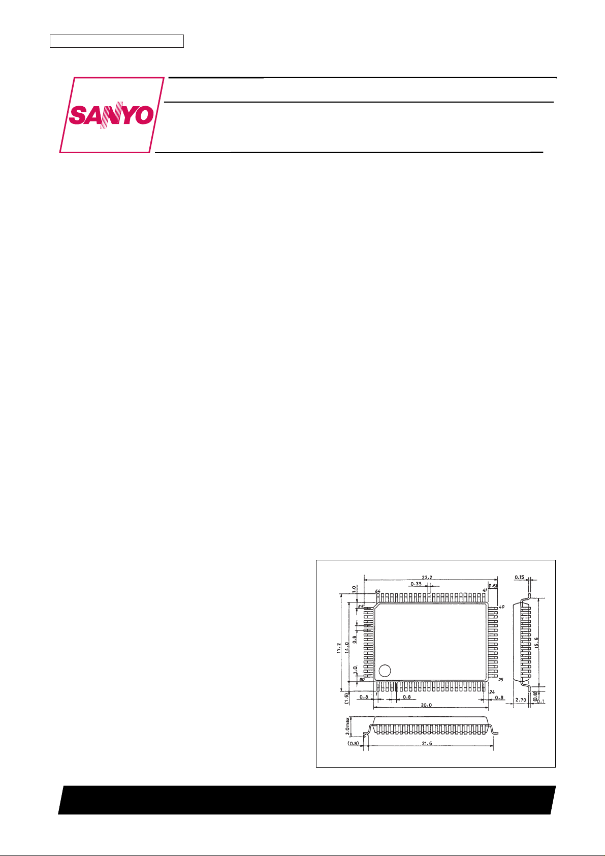
• Package: QFP80E
Package Dimensions
unit: mm
3174-QFP80E
CMOS IC
Ordering number : EN5663
63097HA(OT) No. 5663-1/16
SANYO: QIP80E
[LC83026E]
SANYO Electric Co.,Ltd. Semiconductor Bussiness Headquarters
TOKYO OFFICE Tokyo Bldg., 1-10, 1 Chome, Ueno, Taito-ku, TOKYO, 110 JAPAN
Digital Signal Processor for Karaoke Systems
LC83026E
Page 2
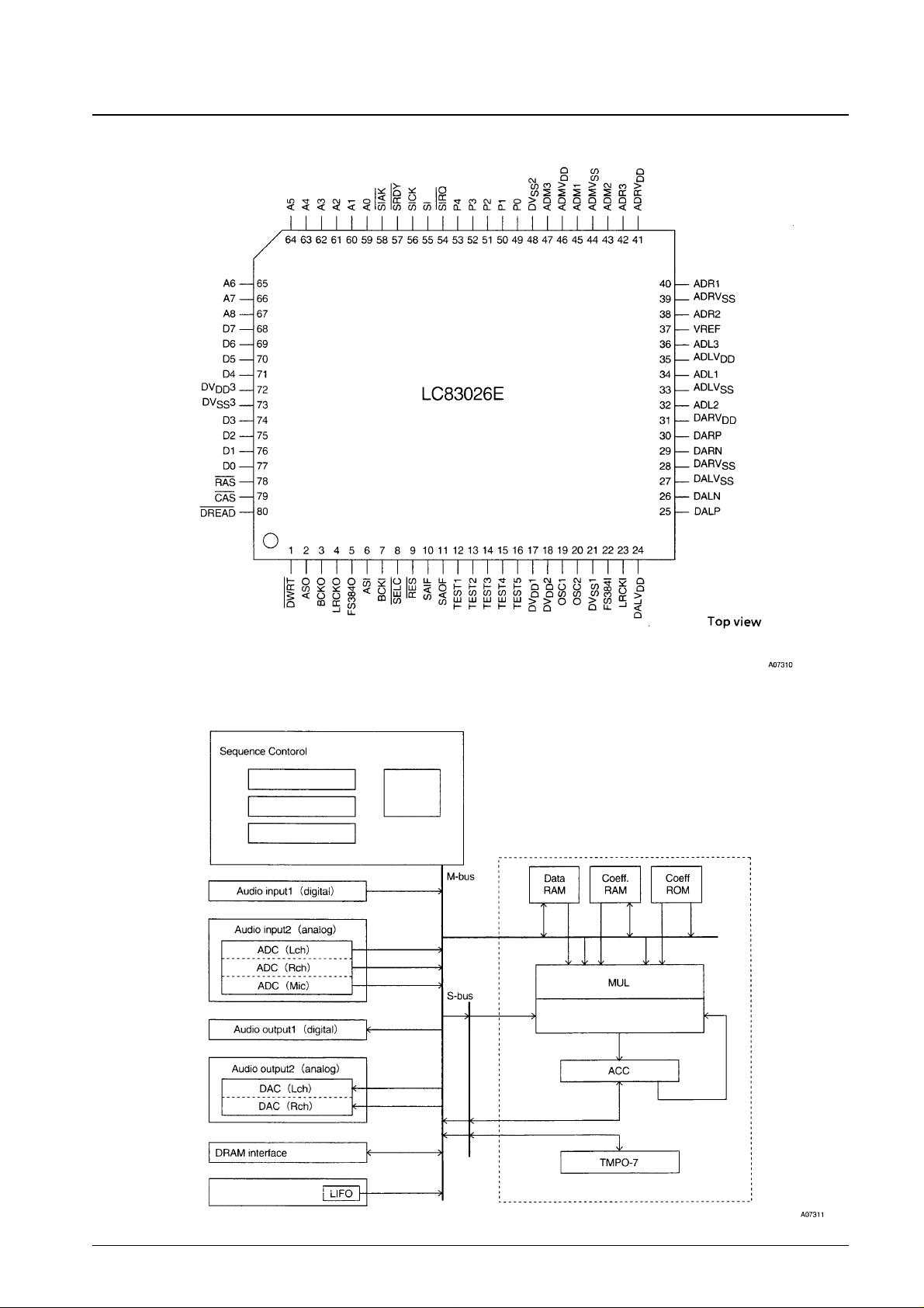
Pin Assignment
Block Diagram
No. 5663-2/16
LC83026E
Microcontroller
interface
Program
decoder
Program ROM
Program counter
Loop counter
Page 3
No. 5663-3/16
LC83026E
Pin Functions
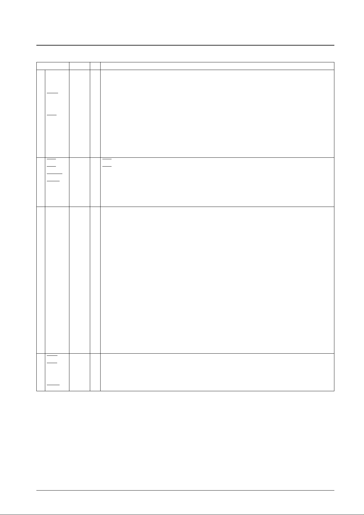
Pin Pin No. I/O Function
OSC1 19 I Crystal oscillator connection (768fs)
OSC2 20 O Crystal oscillator connection (768fs)
FS384I 22 I 384fs input
SELC 8 I Audio clock source switching (High: external, low: internal)
SAIF 10 I Digital audio input mode switching (Low: backward packing, high: forward packing)
SAOF 11 I Digital audio output mode switching (Low: 48fs, high 64fs)
RES 9 I Reset
TEST5 to 1 16 to 12 I Test (Must be connected to ground during normal operation.)
P0 49 I Coefficient transfer mode control
P2 to P1 51, 50 I Initial operating mode control (A high level should be applied for normal operation.)
P3 52 O Microphone signal input level: Yes (low output)/No (high output) output
P4 53 O Music signal input level: Yes (low output)/No (high output) output
RAS 78 O RAS signal output
CAS 79 O CAS signal output
DREAD 80 O External memory read signal output
DWRT 1 O External memory write signal output
A8 to A0 67 to 59 O Address output
D7 to D0 68 to 71, I/O Data input and output (Normally only D0 to D3 are used)
74 to 77
LRCKI 23 I ASI L/R clock input (1fs)
LRCKO 4 O ASO L/R clock output (1fs)
BCKI 7 I ASI bit clock input (32fs or higher)
BCKO 3 O ASO bit clock output (48fs or 64fs)
FS384O 5 O ASO 384fs output
ASI 6 I Digital audio data input (16-bits, MSB first)
ASO 2 O Digital audio data output (16-bits, MSB first, backward packed)
ADL1 34 I A/D converter input (left channel)
ADL2 32 O A/D converter output (left channel)
ADL3 36 O A/D converter output (left channel)
ADR1 40 I A/D converter input (right channel)
ADR2 38 O A/D converter output (right channel)
ADR3 42 O A/D converter output (right channel)
ADM1 45 I A/D converter input (microphone)
ADM2 43 O A/D converter output (microphone)
ADM3 47 O A/D converter output (microphone)
DALP 25 O D/A converter output (left channel)
DALN 26 O D/A converter output (left channel)
DARP 30 O D/A converter output (right channel)
DARN 29 O D/A converter output (right channel)
SIRQ 54 I Input for the serial input request signal
SIAK 58 O Output that indicates that a serial input is in progress
SI 55 I Serial data input from the control microcontroller (8-bit serial input)
SICK 56 I SI pin transfer clock input
SRDY 57 I Ready signal input (from the control microcontroller) that indicates the completion of a serial data input.
Control pins
External memory interface
Audio interface
Microcontroller interface
Continued on next page.
Page 4
No. 5663-4/16
LC83026E
Continued from preceding page.
Pin Pin No. I/O Function
DV
DD
1 to 3 17, 18, 72 — Digital block VDD(Must be connected to +5 V.)
<Make connections as short as possible so that no potential differences occur between any of the V
DD
pins.>
DV
SS
1 to 3 21, 48, 73 — Digital block VSS(Must be connected to ground.)
<Make connections as short as possible so that no potential differences occur between any of the V
SS
pins.>
ADLV
DD
35 — A/D converter VDD(left channel) (Connect to +5 V.)
ADRV
DD
41 — A/D converter VDD(right channel) (Connect to +5 V.)
ADMV
DD
46 — A/D converter VDD(microphone) (Connect to +5 V.)
DALV
DD
24 — D/A converter VDD(left channel) (Connect to +5 V.)
DARV
DD
31 — D/A converter VDD(right channel) (Connect to +5 V.)
ADLV
SS
33 — A/D converter VSS(left channel) (Connect to ground.)
ADRV
SS
39 — A/D converter VSS(right channel) (Connect to ground.)
ADMV
SS
44 — A/D converter VSS(microphone) (Connect to ground.)
DALV
SS
27 — D/A converter VSS(left channel) (Connect to ground.)
DARV
SS
28 — D/A converter VSS(right channel) (Connect to ground.)
Power supply
Design the wiring so that potential differences do
not occur between the analog system V
DD
pins and
either other analog system V
DD
pins or the digital
system V
DD
pins.
Design the wiring so that potential differences do
not occur between the analog system V
SS
pins and
either other analog system V
SS
pins or the digital
system V
SS
pins.
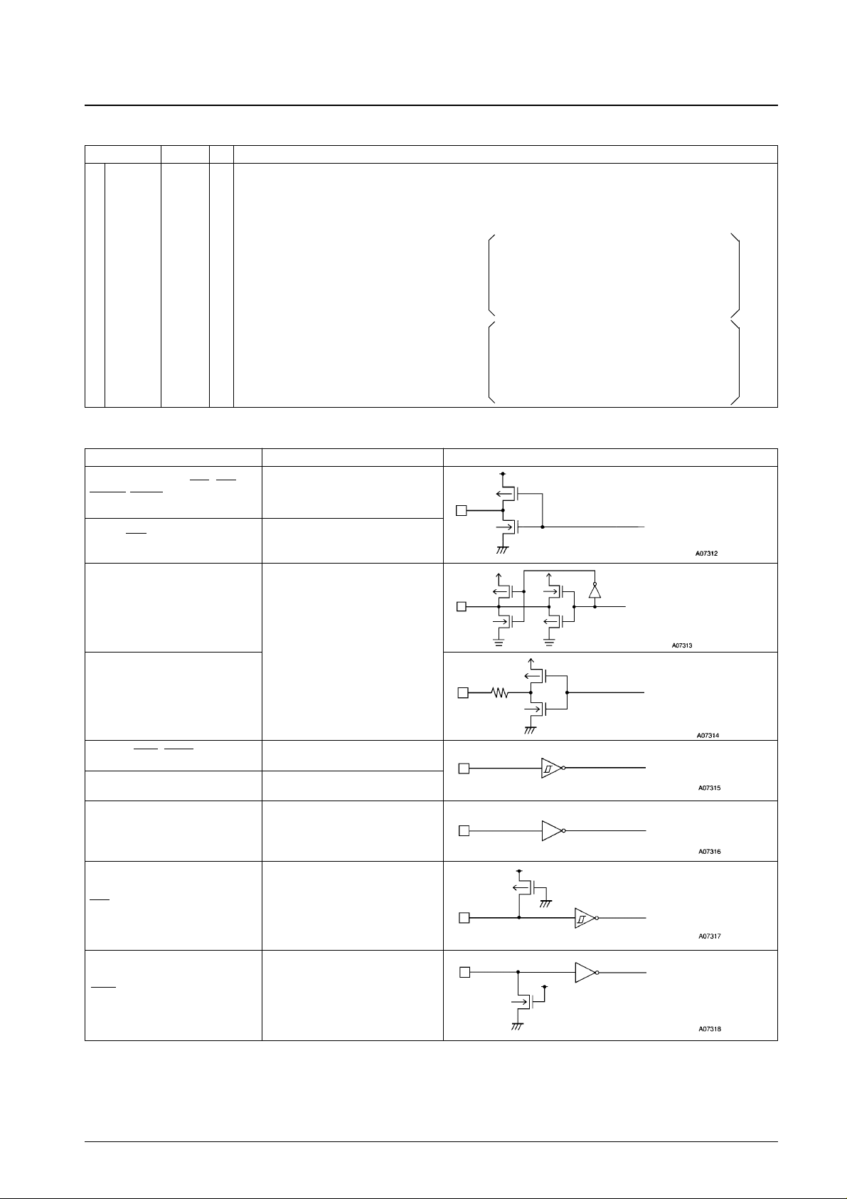
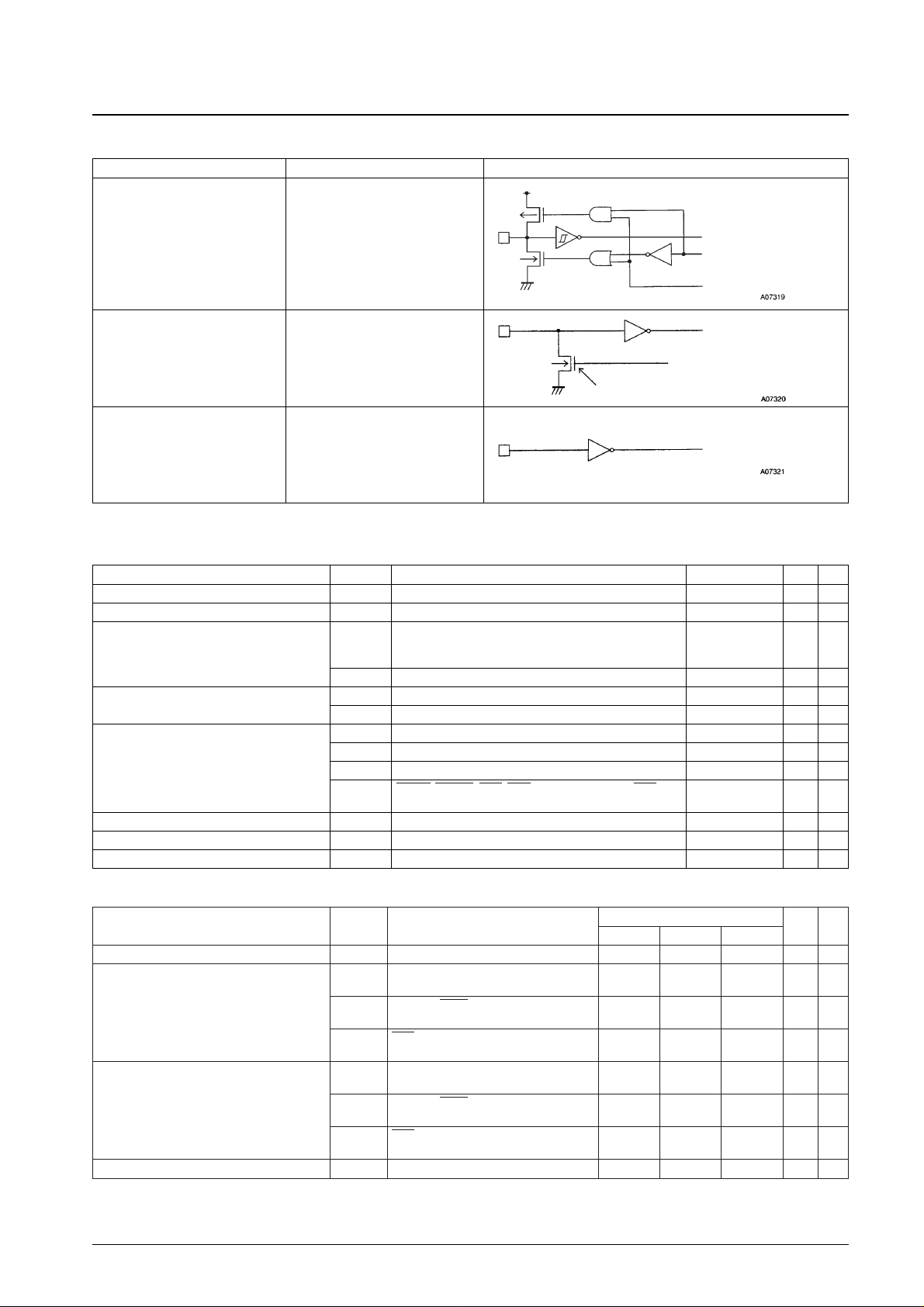
Pin Circuits
Pins Specifications Circuit
ASO, LRCKO, BCKO, RAS, CAS,
DREAD, DWRT, FS384O, A0 to A8
TTL output
ADL2, ADL3, ADM2, ADM3, ADR2,
ADR3
Analog output
Schmitt input
DALP, DALN, DARP, DARN
SI, SICK, SIRQ, SRDY, (OSC1)
Low Schmitt input
FS384I, BCKI, ASI, LRCKI
Normal input
TEST1 to TEST5
Input with built-in pull-up resistor
RES
Input with built-in pull-down resistor
SELC, SAIF, SAOF
P3, P4, SIAK CMOS intermediate current output
Continued on next page.
Output data
Output data
Output data
Input data
Input data
Input data
Input data
Page 5
No. 5663-5/16
LC83026E
Continued from preceding page.
Pins Specifications Circuit
D0 to D7
CMOS intermediate current output
Low Schmitt input
P0 to P2
N-channel open drain intermediate
current output
Normal input
ADL1, ADR1, ADM1 Analog input
Parameter Symbol Conditions Ratings
Unit
Notes
Maximum supply voltage VDDmax –0.3 to +7.0 V
Input voltage V
IN
–0.3 to VDD+0.3 V
Values up to the
VO1 OSC2 output
oscillator voltage are
V
Output voltage
allowable.
VO2 Outputs other than OSC2 –0.3 to VDD+0.3 V
Peak output current
I
OP
1 Audio interface, external RAM interface –2 to +4 mA 1
I
OP
2 Microcontroller interface, P3, P4 –2 to +10 mA 2
I
OA
1 Audio interface, external RAM interface: Per pin –2 to +4 mA 1
I
OA
2 Microcontroller interface, P3, P4: Per pin –2 to +10 mA 2
Average output current ∑I
OA
1 FS384O, LRCKO, BCKO, ASO : Total –10 to +10 mA
∑I
OA
2 DWRT, DREAD, RAS, CAS, A0 to A8, D0 to D7, SIAK,
–10 to +10 mA
P3, P4 : Total
Allowable power dissipation Pd max Ta = –30 to +70°C 700 mW
Operating temperature Topr –30 to +70 °C
Storage temperature Tstg –40 to +125 °C
Specifications
Absolute Maximum Ratings at Ta = 25°C, VSS= 0 V
Parameter Symbol Conditions
Ratings
Unit
Notes
min typ max
Operating supply voltage V
DD
4.75 5.25 V
V
IH
1
Audio interface and external RAM
2.4 V 4
interface
Input high-level voltage VIH2
P0 to P2, SELC, SAIF, SAOF,
0.7 V
DD
V 5
TEST1 to TEST5
VIH3
RES, OSC1, and the microcontroller
0.75 V
DD
V 6
interface
VIL1
Audio interface and external RAM
0.8 V 4
interface
Input low-level voltage
V
IL
2
P0 to P2, SELC, SAIF, SAOF,
0.3 V
DD
V 5
TEST1 to TEST5
VIL3
RES, OSC1, and the microcontroller
0.25 V
DD
V 6
interface
Instruction cycle time t
CYC
58 59.11 ns
Allowable Operating Ranges at Ta = –30 to +70°C, all VDD= 4.75 to 5.25 V, all VSS= 0 V unless otherwise specified
Continued on next page.
Input data
Input data
Input data
Test output data
Off during normal operation
I/O control
Output data
Page 6

Parameter Symbol Conditions
Ratings
Unit
Notes
min typ max
[External Clock Input Conditions]
Frequency f
EXT
Related to the FS384I pin. See Figure 1. 16.85 17.01 MHz
Pulse width
f
EXTH
maximum: 44.1 kHz × 384 × 1.005 23 ns
f
EXTL
minimum: 44.1 kHz × 384 × 0.995 23 ns
Rise time t
EXTR
9 ns
Fall time t
EXF
9 ns
[Self-Excited Oscillation Conditions(crystal oscillator)]
Oscillator frequency f
OSC
OSC1 and OSC2. See Figure 2.
33.84 40.55 MHz
44.1 kHz/48 kHz × 768 ±0.1%
Oscillator stabilization period t
OSCS
See Figure 3. 100 ms
[Audio Data Input Conditions]
Transfer bit clock period t
BCYC
Related to BCKI. See Figure 4. 354 ns
Transfer bit clock pulse width t
BCW
100 ns
Data setup time t
S
70 ns
Data hold time t
H
70 ns
[Serial I/O Clock Conditions]
Serial clock period t
SCYC
480 ns
Serial clock pulse width t
SCW
200 ns
Data setup time t
SS
70 ns
Data hold time t
SH
70 ns
SRDY hold time t
SYH
200 ns
SRDY pulse width t
SYW
200 ns
[DRAM Input Conditions]
Input data setup time t
DSI
20 ns
Input data hold time t
DHI
0 ns
Related to the microcontroller interface.
See Figure 5. (Related to SICK, SI, and
SRDY.)
No. 5663-6/16
LC83026E
Continued from preceding page.
Parameter Symbol Conditions
Ratings
Unit
Notes
min typ max
SELC, SAIF, SAOF,
IIH1 VIN= VDD(Input pins with pull-down 100 250 µA 8
Input high-level current
resistors)
IIH2 P0 to P2, VIN= VDD(Nch transistor OFF) 10 µA
I
IH
3 Other input-only pins 10 µA
I
IL
1
RES, V
IN
= VSS(Input pins with pull-up
–250 –100 µA 8
resistors)
Input low-level current
IIL2 P0 to P2, VIN= V
SS
–10 µA
I
IL
3 Other input-only pins –10 µA
Output high-level voltage
V
OH
1 IOH= –0.4 mA 4.0 4.98 V 1, 8
V
OH
2 IOH= –50 µA VDD–1.2 4.997 V 2,3,8
Output low-level voltage
V
OL
1 IOL= 2 mA 0.065 0.4 V 1, 8
V
OL
2 IOL= 10 mA 0.32 1.5 V 2,3,8
Output off leakage current I
OFFVO
= VSS, V
DD
–40 +40 µA
Input and output capacitance C
IO
10 pF
[Audio Data Output Timing]
Output data hold time t
OH
–30 ns 7
Output data delay time t
OD
50 ns 7
Electrical Characteristics 1 at Ta = –30 to +70°C, all VDD= 4.75 to 5.25 V, all VSS= 0 V unless otherwise specified
Continued on next page.
Related to external DRAM data input. See
Figure 6. (Related to CAS and D0 to D7.)
BCK0 and ASO. See Figure 7.
Page 7

No. 5663-7/16
LC83026E
Parameter Symbol Conditions
Ratings
Unit
Notes
min typ max
[External DRAM Access Timing]
RAS high-level pulse width t
RP
80 ns 7
RAS low-level pulse width t
RAS
700 ns 7
CAS high-level pulse width t
CP
50 ns 7
CAS low-level pulse width t
CAS
95 ns 7
CAS cycle time t
PC
175 ns 7
RAS to CAS delay time t
RCD
60 ns 7
CAS hold time t
CSH
170 ns 7
RAS hold time t
RSH
95 ns 7
RAS address setup time t
ASR
60 ns 7
RAS address hold time t
RAH
20 ns 7
CAS address setup time t
ASC
30 ns 7
CAS address hold time t
CAH
90 ns 7
DWRT pulse width t
WP
95 ns 7
Write command setup time t
WCS
12 ns 7
Write command hold time t
WCH
65 ns 7
Output data setup time t
DSO
30 ns 7
Output data hold time t
DHO
100 ns 7
C1 13 pF 8
Crystal oscillator C2 29 pF 8
L 1.5 µH 8
Current drain I
DD
60 95 mA 9
Continued from preceding page.
Parameter Symbol Conditions
Ratings
Unit
Notes
min typ max
[A/D Converter Block]
Total harmonic distortion A-THD 1 kHz, at 0 dB 0.05 % 10
Signal-to-noise ratio A-S/N 1 kHz, at 0 dB 75 80 dB 10,11
Crosstalk A-C · T 1 kHz, at 0 dB –75 dB 10,11
[D/A Converter Block]
Total harmonic distortion D-THD 1 kHz, at 0 dB 0.01 % 10
Signal-to-noise ratio D-S/N 1 kHz, at 0 dB 85 dB 10,11
Crosstalk D-C · T 1 kHz, at 0 dB –80 dB 10,11
Electrical Characteristics 2 at Ta = 25°C, all VDD= 5.0 V, all VSS= 0 V unless otherwise specified
Notes: 1. TTL output level pins: ASO, FS384O, BCKO, LRCKO, D0 to D7, A0 to A8, RAS, CAS, DREAD, DWRT
2. CMOS intermediate current output pins: P3, P4, SIAK
3. N-channel open drain intermediate current output pins: P0 to P2
4. Low Schmitt input pins: BCKI, ASI, LRCKI, D0 to D7, FS384I
5. Normal input pins: P0 to P2, TEST1 to TEST5, SELC, SAIF, SAOF
6. Schmitt input pins: RES, SI, SICK, SIRQ, SRDY, OSC1
7. When the load capacitance is 50 pF.
8. The values for the oscillator capacitors C1 and C2 include the line capacitances.
9. The typical values for the current drain are for V
DD
= 5 V, room temperature, and typical samples.
10. Fs = 44.1 kHz and 20 kHz low-pass filter used. Measurement is with the external circuit structure and constants in the Sanyo evaluation board.
11. With the weight A filter used.
Output timing to the external DRAM.
See Figure 8.
Output timing to the external DRAM.
See Figure 8.
OSC1 and OSC2. See Figure 2.
For V
DD
1, VDD2, and VDD3 when
operating at 33.8688 MHz.
Page 8

Figure 5 Microcontroller Interface
No. 5663-8/16
LC83026E
Figure 1 External Clock Input Waveform (FS384I)
Figure 2 Crystal Oscillator Circuit
Figure 3 Oscillator Stabilization Time
Figure 4 Audio Data Input Conditions
Lower limit of the
operating V
DD
Oscillator
stabilization time
Stable oscillation
Transfer bit clock
(BCKI)
Input data
(ASI)
Serial clock
(SICK)
Transfer
complete
(SRDY)
Input data
(SI)
Page 9

No. 5663-9/16
LC83026E
Figure 7 Audio Data Output Timing
Figure 8 External DRAM Data Output Timing
Differences between the LC83025E and the LC83026E
Parameter LC83025E LC83026E
Decimation filter improved
Input comparator improved
A/D converter block
*: The V
REF
pin was added in association with the improvements to the input comparator. The V
REF
pin external
capacitor must be located as close as possible to the LC83026E, and must be connected with lines that are as
short as possible.
4 × oversampling filters used 2 × oversampling filters used
D/A converter block Second-order noise shaping Third-order noise shaping
Single-pin output used. Two-pin output operation
Reset time One or more sampling period Two or more sampling periods
When no digital input is provided The LRCKI and BCKI pins must be connected to the
The LRCKI and BCKI pins must be connected to either
(when the SELC pin is low) LRCKO and BCKO pins.
V
DD
or VSS; they do not need to be connected to the
LRCKO and BCKO pins.
Figure 6 External DRAM Data Input Timing
(A0 to A8)
(D0 to D3)
Transfer bit clock
(BCKO)
Output data
(ASO)
(A0 to A8)
(D0 to D3)
Page 10

Overall Signal Flow
No. 5663-10/16
LC83026E
Voice mute
Pitch shifter
Surround
Clip
processing
A margin of 1 bit
DC cut high-pass filter
Micro-
phone
echo
Clip
processing
Clip
processing
Clip
processing
Bass
Page 11

Figure 9 A/D Converter External Circuit Example
No. 5663-11/16
LC83026E
*: The V
REF
pin capacitor must be
located as close as possible to
the IC.
Note: All external circuits should
be located as close as
possible to the IC.
Page 12

Figure 10 D/A Converter External Circuit Example
No. 5663-12/16
LC83026E
Identical to the left channel circuit
Right channel
output
Left channel
output
Page 13

Application Circuit Example Outline (When digital input is not used)
No. 5663-13/16
LC83026E
The values of 29
and 13 pF here
include the
printed circuit
board
capacitances.
A/D converter
external circuit
(left channel)
D/A converter
external circuit
(left channel)
D/A converter
external circuit
(right channel)
D/A converter
A/D converter
external circuit
(right channel)
A/D converter
external circuit
(microphone)
Microcontroller
(Coefficient transfer mode control pin)
(Initial mode selection pins)
(Microphone input level display pin)
(Music input level display pin)
Whether or not the digital inputs and/or analog outputs are used depends on the
specifications of the application.
If any of these pins are not used, any unused input pins should be tied to high or low and any
unused output pins should be left open.
A0 to A8
D0 to D3
DVDD1 to DVDD3
DVSS1 to DVSS3
D4 to D7
TEST1 to TEST5
Page 14

Application Circuit Example Outline (When digital input is used 1)
No. 5663-14/16
LC83026E
The values of 29
and 13 pF here
include the
printed circuit
board
capacitances.
A/D converter
external circuit
(left channel)
D/A converter
external circuit
(left channel)
D/A converter
external circuit
(right channel)
D/A converter
CD-DSP or
other circuit
Apply high or low levels to these
pins according to the audio
interface mode used.
A/D converter
external circuit
(right channel)
A/D converter
external circuit
(microphone)
Microcontroller
(Coefficient transfer mode control pin)
(Initial mode selection pins)
(Microphone input level display pin)
(Music input level display pin)
Whether or not the digital inputs and/or analog outputs are used depends on the
specifications of the application.
If any of these pins are not used, any unused input pins should be tied to high or low and any
unused output pins should be left open.
Divide-bytwo circuit
D4 to D7
DVDD1 to DVDD3
DVSS1 to DVSS3
A0 to A8
D0 to D3
TEST1 to TEST5
Page 15

No. 5663-15/16
LC83026E
Application Circuit Example Outline (When digital input is used 2)
The values of 29
and 13 pF here
include the
printed circuit
board
capacitances.
A/D converter
external circuit
(left channel)
D/A converter
external circuit
(left channel)
D/A converter
external circuit
(right channel)
D/A converter
CD-DSP or
other circuit
Apply high or low levels to these
pins according to the audio
interface mode used.
A/D converter
external circuit
(right channel)
A/D converter
external circuit
(microphone)
Microcontroller
(Coefficient transfer mode control pin)
(Initial mode selection pins)
(Microphone input level display pin)
(Music input level display pin)
Whether or not the digital inputs and/or analog outputs are used depends on the
specifications of the application.
If any of these pins are not used, any unused input pins should be tied to high or low
and any unused output pins should be left open.
D4 to D7
DVDD1 to DVDD3
DVSS1 to DVSS3
A0 to A8
D0 to D3
TEST1 to TEST5
Page 16

No. 5663-16/16
LC83026E
This catalog provides information as of June, 1997. Specifications and information herein are subject to change
without notice.
■ No products described or contained herein are intended for use in surgical implants, life-support systems, aerospace
equipment, nuclear power control systems, vehicles, disaster/crime-prevention equipment and the like, the failure of
which may directly or indirectly cause injury, death or property loss.
■ Anyone purchasing any products described or contained herein for an above-mentioned use shall:
➀ Accept full responsibility and indemnify and defend SANYO ELECTRIC CO., LTD., its affiliates, subsidiaries and
distributors and all their officers and employees, jointly and severally, against any and all claims and litigation and all
damages, cost and expenses associated with such use:
➁ Not impose any responsibility for any fault or negligence which may be cited in any such claim or litigation on
SANYO ELECTRIC CO., LTD., its affiliates, subsidiaries and distributors or any of their officers and employees
jointly or severally.
■ Information (including circuit diagrams and circuit parameters) herein is for example only; it is not guaranteed for
volume production. SANYO believes information herein is accurate and reliable, but no guarantees are made or implied
regarding its use or any infringements of intellectual property rights or other rights of third parties.
 Loading...