

Page 1
CMOS LSI
Ordering number : EN4977A
62896HA (OT)/63095HA (OT) No. 4977-1/15
SANYO Electric Co.,Ltd. Semiconductor Bussiness Headquarters
TOKYO OFFICE Tokyo Bldg., 1-10, 1 Chome, Ueno, Taito-ku, TOKYO, 110 JAPAN
Digital Signal Processor
for Karaoke Products
LC83025E
Overview
The LC83025E is a special-purpose karaoke DSP that
implements the signal processing required by karaoke
systems, including pitch shift, microphone echo, voice
muting and simple surround, with only a single 256Kb
external DRAM. Since the LC83025E includes built-in
A/D and D/A converters, it can also handle analog inputs
and outputs in addition to digital inputs and outputs. The
LC83025E uses serial transfer of coefficient data from a
microcontroller to handle changes in functions and
characteristics required for each application.
Features
• Applications
— Pitch shift
The LC83025E can shift the music pitch or the
microphone pitch by ±15 steps in 1/4 interval steps,
or ±1 octave in scale tone steps according to
command data sent from the microcontroller.
Furthermore, the pitch can be changed up to ±1
octave in arbitrary steps by setting internal
coefficients.
— Microphone echo
The LC83025E implements echo processing for the
signal input from the microphone A/D converter.
The amount of echo, the delay time and other
parameters can be changed by setting coefficients.
— Voice mute
The LC83025E implements processing that removes
monaural signal components included in the music
signal. This allows CDs with vocals to be used as
karaoke CDs. Command data is used to turn the
voice mute function on or off.
— Simple surround
The LC83025E implements a simple surround
function by adding delayed components to the music
signal. The LC83025E includes six sets of simple
surround coefficients as built-in preset data. These
values can be switched by sending command data.
Applications can implement their own original
surround effects by setting the coefficients.
However, the algorithm itself is fixed.
— Flexible input mixing
The LC83025E supports hybrid mixing of digital
and analog left and right channel song inputs, and
thus can handle a wide range of disk processing
configurations.
• Audio inputs and outputs
— Inputs: Digital - One system (stereo)
A/D converter - Three channels
— Outputs: Digital - One system (stereo)
D/A converter - Two channels
— A/D converter
Second order ∆∑ modulation - Three channels
— D/A converter
4× oversampling digital filters
plus second order noise shaper
plus 5-bit PWM system - Two channels
• Master clock: 768 fs
• External memory: Up to two 256K (64K × 4-bit)
DRAMs can be used
• Microcontroller input: Synchronous 8-bit serial data
• Supply voltage: 5 V single-voltage
• Package: QFP80E
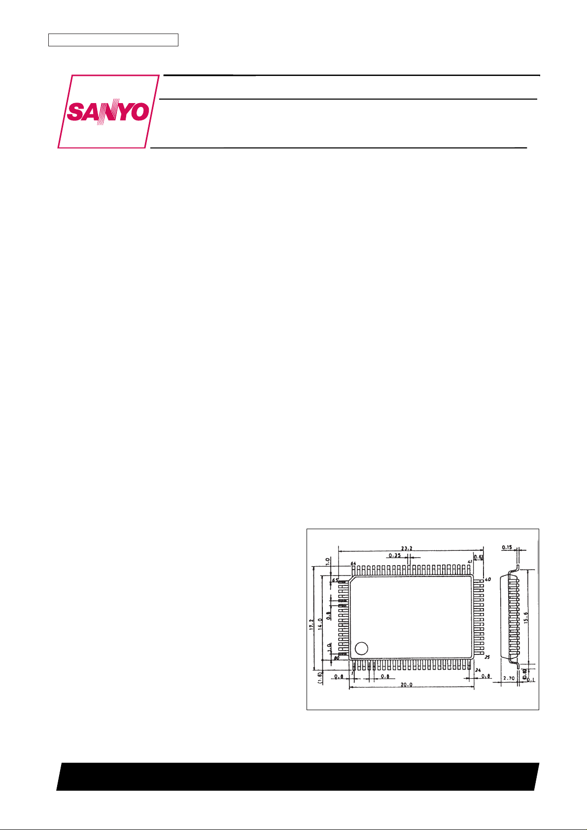
Package Dimensions
unit: mm
3174-QFP80E
SANYO: QFP80E
[LC83025E]
Page 2
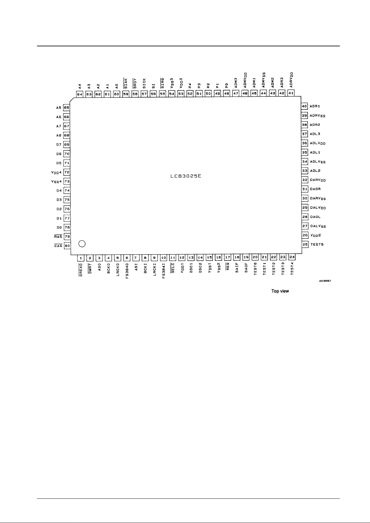
Pin Assignment
No. 4977-2/15
LC83025E
Page 3
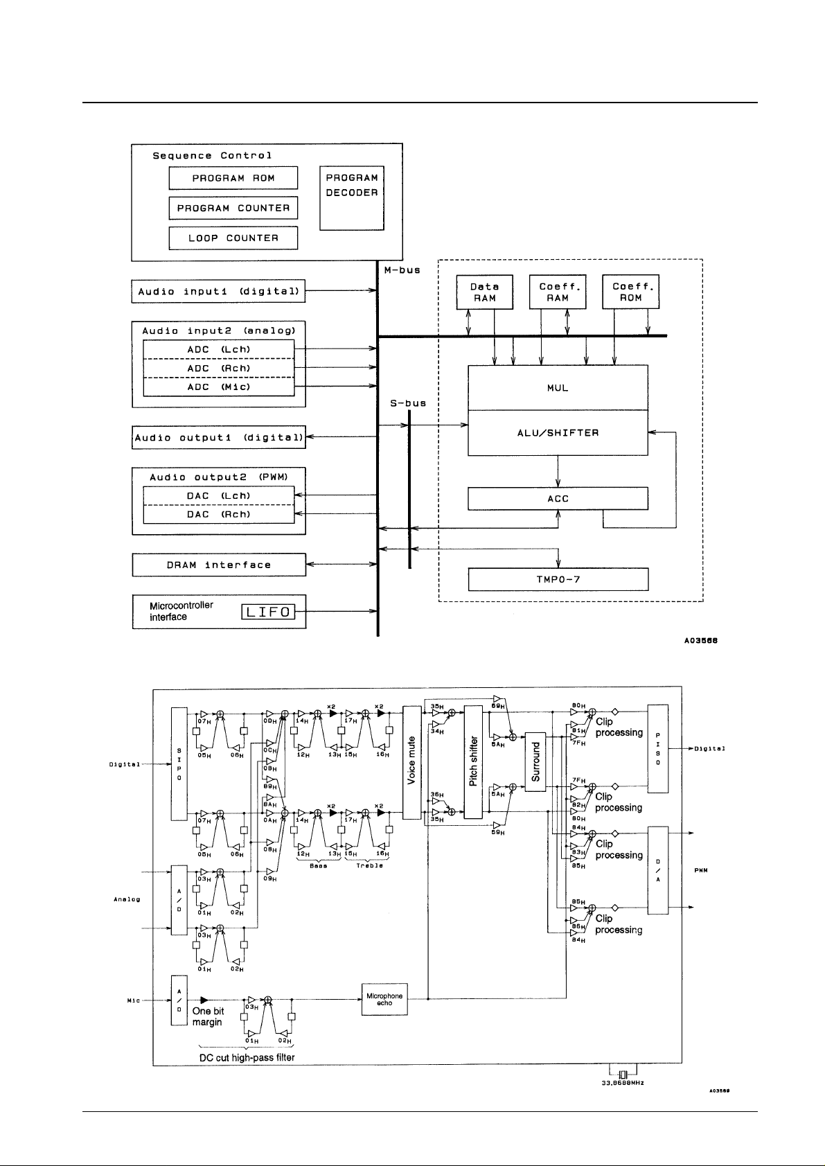
Block Diagram
Signal Flow Overview
No. 4977-3/15
LC83025E
Page 4
Pin Functions
No. 4977-4/15
LC83025E
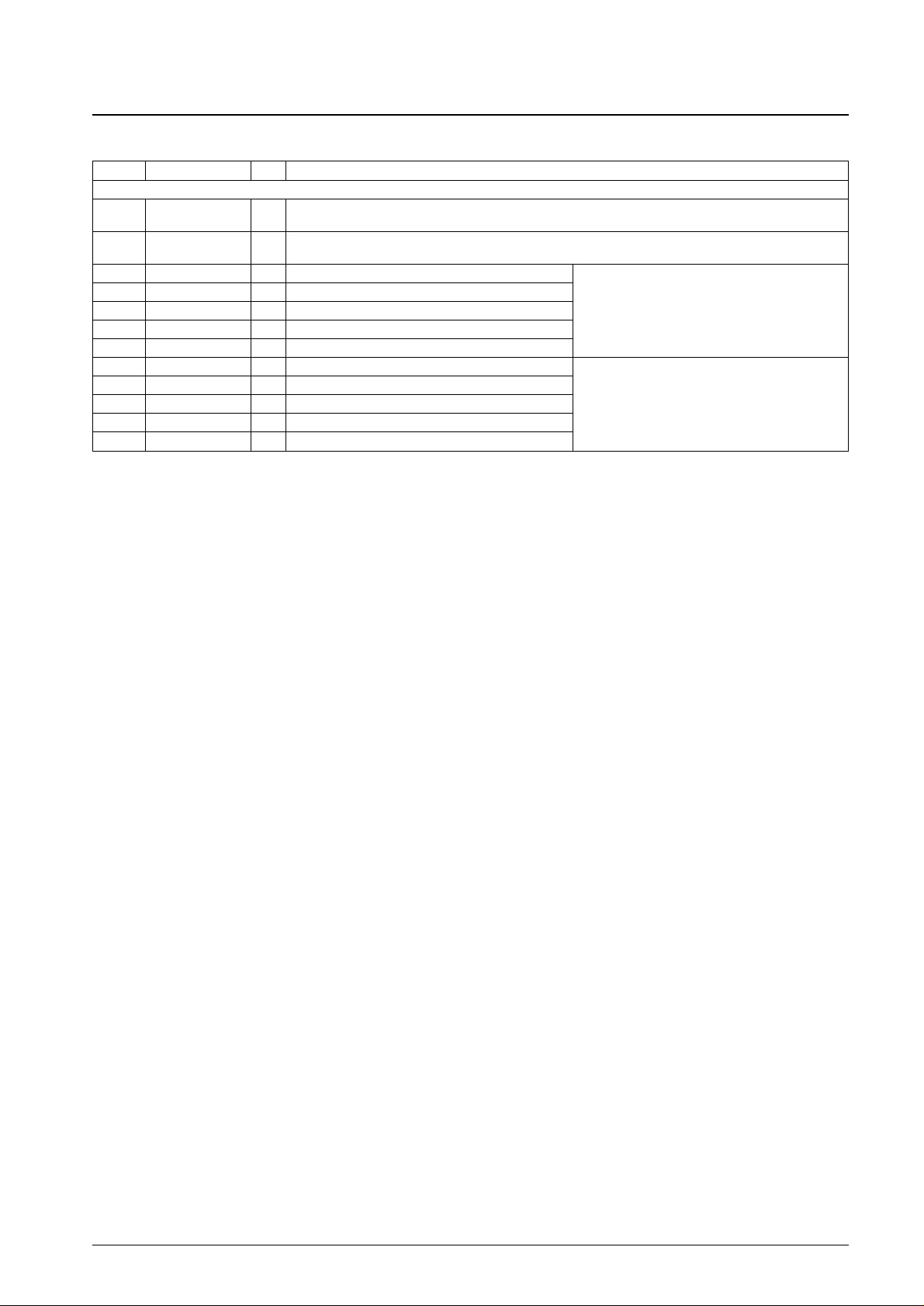
Pin No. Symbol I/O Function
[Control pins]
13 OSC1 I Crystal oscillator connection (768 fs)
14 OSC2 O Crystal oscillator connection (768 fs)
10 FS384I I 384 fs input (Apply a clock that is equal to the OSC1/OSC2 768 fs clock divided by 2.)
11 SELC I Audio clock source switching (High: Fixes FS384I as the clock)
18 SAIF I Digital audio input mode switching (Low: backward packed, High: forward packed)
19 SAOF I Digital audio output mode switching (Low: 48 fs, High: 64 fs)
17 RES I Reset
25 to 21
TEST5 to
I Test (Must be tied to ground in normal operation.)
TEST1
20 TEST6 O Test (Must be left open in normal operation.)
48 P0 I Coefficient transfer mode switching
50, 49 P2, P1 I Initial operating mode setting (This pin should be held high in normal operation.)
51 P3 O Microphone signal present (low output) or absent (high output) indication output
52 P4 O Music signal present (low output) or absent (high output) indication output
[External memory interface]
79 RAS O RAS signal output
80 CAS O CAS signal output
1 DREAD O External memory read signal output
2 DWRT O External memory write signal output
68 to 60 A8 to A0 O Address outputs
69 to 71,
D7 to D0 I/O Data I/O (Normally, only D3 to D0 are used.)
74 to 78
[Audio interface]
9 LRCKI I ASI L/R clock input (1 fs)
5 LRCKO O ASO L/R clock output (1 fs)
8 BCKI I ASI bit clock input (32 fs or higher)
4 BCKO O ASO bit clock output (48 fs or 64 fs)
6 FS384O O ASO 384 fs output
7 ASI I Digital audio data input (MSB first, 16 bits)
3 ASO O Digital audio data output (MSB first, backward packed, 16 bits)
35 ADL1 I A/D converter input (left channel)
33 ADL2 O A/D converter output (left channel)
37 ADL3 O A/D converter output (left channel)
40 ADR1 I A/D converter input (right channel)
38 ADR2 O A/D converter output (right channel)
42 ADR3 O A/D converter output (right channel)
45 ADM1 I A/D converter input (microphone)
43 ADM2 O A/D converter output (microphone)
47 ADM3 O A/D converter output (microphone)
28 DAOL O D/A converter output (left channel)
31 DAOR O D/A converter output (right channel)
[Microcontroller interface]
55 SIRQ I Serial input request signal input
59 SIAK O Output indicating serial input execution in progress
56 SI I Serial data input from the control microcontroller (8-bit serial data)
57 SICK I SI transfer clock input
58 SRDY I Ready signal input from the control microcontroller that indicates that serial data input has completed
Continued on next page.
Page 5
Continued from preceding page.
No. 4977-5/15
LC83025E
Pin No. Symbol I/O Function
[Power supply pins]
12, 26,
V
DD
—
V
DD
for the digital block (Connect to +5 V.)
53, 72 (Keep connections as short as possible so that potential differences between the V
DD
pins do not occur.)
15, 16,
V
SS
—
V
SS
for the digital block (Connect to ground.)
54, 73 (Keep connections as short as possible so that potential differences between the V
SS
pins do not occur.)
36 ADLV
DD
— A/D converter VDD(left channel) (Connect to +5 V.)
41 ADRV
DD
— A/D converter VDD(right channel) (Connect to +5 V.)
46 ADMV
DD
— A/D converter VDD(microphone) (Connect to +5 V.)
29 DALV
DD
— D/A converter VDD(left channel) (Connect to +5 V.)
32 DARV
DD
— D/A converter VDD(right channel) (Connect to +5 V.)
34 ADLV
SS
— A/D converter VSS(left channel) (Connect to ground.)
39 ADRV
SS
— A/D converter VSS(right channel) (Connect to ground.)
44 ADMV
SS
— A/D converter VSS(microphone) (Connect to ground.)
27 DALV
SS
— D/A converter VSS(left channel) (Connect to ground.)
30 DARV
SS
— D/A converter VSS(right channel) (Connect to ground.)
Design the application wiring so
that potential differences do not
occur between the analog V
SS
pins and between the digital V
SS
group and the analog VSSgroup.
Design the application wiring so
that potential differences do not
occur between the analog V
DD
pins and between the digital V
DD
group and the analog VDDgroup.
Page 6

Pin Circuits
No. 4977-6/15
LC83025E
Specification Circuit Pins
TTL output
CMOS intermediate
current output
Analog output
Schmitt input
Low Schmitt input
Normal input
Input with built-in
pull-up resistor
Input with built-in
pull-down resistor
CMOS intermediate
current output
Low Schmitt input
N-channel open drain
intermediate current output
Normal input
Analog input
ASO, LRCKO, BCKO, RAS, CAS, DREAD, DWRT,
FS384O, A0 to A8
P3, P4, SIAK, TEST6
DAOL, DAOR, ADL2, ADL3, ADM2, ADM3, ADR2, ADR3
SI, SICK, SIRQ, SRDY, (OSC1)
FS384I, BCKI, ASI, LRCKI
TEST1 to TEST5
RES
SELC, SAIF, SAOF
D0 to D7
P0 to P2
ADL1, ADR1, ADM1
Page 7

Specifications
Absolute Maximum Ratings at Ta = 25°C, VSS= 0 V
Allowable Operating Ranges
at Ta = –30 to +70°C, all VDD= 4.75 to 5.25 V, all VSS= 0 V unless otherwise specified
No. 4977-7/15
LC83025E
Parameter Symbol Conditions Ratings Unit Note
Maximum supply voltage V
DD
max –0.3 to +7.0 V
V
O
1 OSC2 output
Allowed up to the
V
Output voltage
oscillator voltage.
V
O
2 Pins other than OSC2 –0.3 to VDD+ 0.3 V
Input voltage V
IN
–0.3 to VDD+ 0.3 V
Peak output current
I
OP
1 Audio interface, external RAM interface –2 to +4 mA 1
I
OP
2 Microcontroller interface, P3, P4 –2 to +10 mA 2
I
OA
1 Audio interface, external RAM interface: per pin –2 to +4 mA 1
I
OA
2 Microcontroller interface, P3, P4: per pin –2 to +10 mA 2
Average output current
ΣI
OA
1 Total for FS384O, LRCKO, BCKO, and ASO –10 to +10 mA
ΣI
OA
2
Total for DWRT, DREAD, RAS, CAS, A3 to A8
–30 to +30 mA
and D0 to D7
ΣI
OA
3 Total for A0 to A2, SIAK, P3 and P4 –10 to +10 mA
Allowable power dissipation Pd max Ta = –30 to +70°C 700 mW
Operating temperature Topr –30 to +70 °C
Storage temperature Tstg –40 to +125 °C
Parameter Symbol Conditions min typ max Unit Note
Operating supply voltage V
DD
4.75 5.25 V
V
IH
1 Audio interface, external RAM interface 2.4 V 4
Input high level voltage V
IH
2 P0 to P2, SELC, SAIF, SAOF, TEST1 to TEST5 0.7 V
DD
V 5
V
IH
3 RES, OSC1, microcontroller interface 0.75 V
DD
V 6
V
IL
1 Audio interface, external RAM interface 0.8 V 4
Input low level voltage V
IL
2 P0 to P2, SELC, SAIF, SAOF, TEST1 to TEST5 0.3 V
DD
V 5
V
IL
3 RES, OSC1, microcontroller interface 0.25 V
DD
V 6
Instruction cycle time t
CYC
58 59.11 ns
[External Clock Input Conditions]
Frequency f
EXT
16.85 17.01 MHz
Pulse width
t
EXTH
23 ns
t
EXTL
23 ns
Rise time t
EXTR
9 ns
Fall time t
EXTF
9 ns
[Self-Excitation Oscillation Conditions]
Oscillator frequency f
OSC
OSC1 and OSC2: shown in Figure 2.
33.84 33.90 MHz
44.1 kHz × 768 × ± 0.1%
Oscillator stabilization period f
OSCS
Shown in Figure 3. 100 ms
[Audio Data Input Conditions]
Transfer bit clock period t
BCYC
354 ns
Transfer bit clock pulse width t
BCW
Related to the BCKI and ASI pins. Shown in Figure 4.
100 ns
Data setup time t
S
70 ns
Data hold time t
H
70 ns
[Serial Input Clock Conditions]
Serial clock period t
SCYC
480 ns
Serial clock pulse width t
SCW
200 ns
Data setup time t
SS
Related to the microcontroller interface. Shown in
70 ns
Data hold time t
SH
Figure 5. (Related to the SICK, SI and SRDY pins.)
70 ns
SRDY hold time t
SYH
200 ns
SRDY pulse width t
SYW
200 ns
[DRAM Input Conditions]
Input data setup time t
DSI
Related to external DRAM data input. Shown in Figure 6.
20 ns
Input data hold time t
DHI
(Related to the CAS and D0 to D7 pins.)
0 ns
Related to the FS384I pin. Shown in Figure 1.
max: 44.1 kHz × 384 × 1.005
min: 44.1 kHz × 384 × 0.995
Page 8

Electrical Characteristics 1
at Ta = –30 to +70°C, all VDD= 4.75 to 5.25 V, all VSS= 0 V unless otherwise specified
No. 4977-8/15
LC83025E
Parameter Symbol Conditions min typ max Unit Note
I
IL
1 RES, VIN= VSS(Input pins with built-in pull-up resistor) –250 –100 µA 8
Input low level current I
IL
2 P0 to P2, VIN= V
SS
–10 µA
I
IL
3 Other input-only pins –10 µA
I
IH
1
SELC, SAIF, SAOF, V
IN
= V
DD
100 250 µA 8
Input high level current
(Input pins with built-in pull-down resistor)
I
IH
2 P0 to P2, VIN= VDD(n-channel transistor: off) 10 µA
I
IH
3 Other input-only pins 10 µA
Output high level voltage
V
OH
1 IOH= –0.4 mA 4.0 4.98 V 1, 8
V
OH
2 IOH= –50 µA VDD– 1.2 4.997 V 2, 3, 8
Output low level voltage
V
OL
1 IOL= 2 mA 0.065 0.4 V 1, 8
V
OL
2 IOL= 10 mA 0.32 1.5 V 2, 3, 8
Output off leakage current I
OFF
VO= VSS, V
DD
–40 +40 µA
I/O capacitance C
IO
10 pF
[Audio Data Output Timing]
Output data hold time t
OH
BCKO and ASO: shown in Figure 7.
–30 ns 7
Output data delay time t
OD
50 ns 7
[External DRAM Access Timing]
RAS high pulse width t
RP
80 ns 7
RAS low pulse width t
RAS
700 ns 7
CAS high pulse width t
CP
50 ns 7
CAS low pulse width t
CAS
95 ns 7
CAS cycle time t
PC
175 ns 7
RAS to CAS delay time t
RCD
60 ns 7
CAS hold time t
CSH
170 ns 7
RAS hold time t
RSH
Timing for output to the external DRAM.
95 ns 7
RAS address setup time t
ASR
Shown in Figure 8.
60 ns 7
RAS address hold time t
RAH
20 ns 7
CAS address setup time t
ASC
30 ns 7
CAS address hold time t
CAH
90 ns 7
DWRT pulse width t
WP
95 ns 7
Write command setup time t
WCS
12 ns 7
Write command hold time t
WCH
65 ns 7
Output data setup time t
DSO
30 ns 7
Output data hold time t
DHO
100 ns 7
Crystal oscillator
C1
OSC1 and OSC2: shown in Figure 2.
13 pF 8
C2 29 pF 8
Current drain
L
V
DD
1, VDD2, VDD3; oscillator frequency: 33.8688 MHz
1.5 µH 8
I
DD
60 95 mA 9
Page 9

Electrical Characteristics 2 at Ta = 25°C, all VDD= 5.0 V, all VSS= 0 V unless otherwise specified
Note: 1. TTL output level pins: ASO, FS384O, BCKO, LRCKO, D0 to D7, A0 to A8, RAS, CAS, DREAD, DWRT
2. CMOS intermediate current output pins: P3, P4, SIAK, TEST6
3. N-channel open-drain intermediate current output pins: P0 to P2
4. Low Schmitt input pins: BCKI, ASI, LRCKI, D0 to D7, FS384I
5. Normal input pins: P0 to P2, TEST1 to TEST5, SELC, SAIF, SAOF
6. Schmitt input pins: RES, SI, SICK, SIRQ, SRDY, OSC1
7. When the load capacitance is 50 pF
8. The values for the oscillator capacitors C1 and C2 include the wiring capacitances.
9. The value for the current drain is a typical value for V
DD
= 5 V, room temperature, and a typical sample.
10. With weight A filter present, with Fs = 44.1 kHz, and tested in the Sanyo evaluation board.
11. Varies with the values of the external components. The listed value is for the circuit structure and values shown in Figure 9 in the Sanyo evaluation
board.
Figure 1 External Clock Input Waveform (FS384I) Figure 2 Crystal Oscillator Circuit
Figure 3 Oscillator Stabilization Time
No. 4977-9/15
LC83025E
Parameter Symbol Conditions min typ max Unit Note
[A/D Converter Block]
1 kHz, 0 dB: Lch 0.065 % 10, 11
Total harmonic distortion A-THD 1 kHz, 0 dB: Rch 0.065 % 10, 11
1 kHz, 0 dB: Mic 0.070 % 10, 11
Signal-to-noise ratio A-S/N 1 kHz, 0 dB 70 75 dB 10, 11
Crosstalk A-C · T 1 kHz, 0 dB –72 dB 10
[D/A Converter Block]
Total harmonic distortion D-THD 1 kHz, –1 dB 0.045 % 10
Signal-to-noise ratio D-S/N 1 kHz, –1 dB 78 dB 10
Crosstalk D-C · T 1 kHz, –1 dB –75 dB 10
Page 10

Figure 4 Audio Data Input Conditions
Figure 5 Microcontroller Interface
Figure 6 Timing for Data Input from External DRAM
Figure 7 Audio Data Output Timing
No. 4977-10/15
LC83025E
Page 11

Figure 8 Timing for Data Output to External DRAM
Figure 9 Sample A/D Converter External Circuit
No. 4977-11/15
LC83025E
Page 12

Figure 10 Sample D/A Converter External Circuit
No. 4977-12/15
LC83025E
Page 13

Sample Peripheral Circuit Connection (For applications that do not use digital input)
Whether or not the digital outputs and the analog L/R outputs will be used will be determined by the end product
specifications. These pins should be left open if unused.
No. 4977-13/15
LC83025E
Page 14

No. 4977-14/15
LC83025E
Sample Peripheral Circuit Connection (For applications that use digital input.)
Whether or not the analog L/R inputs and the analog L/R outputs will be used will be determined by the end product
specifications. A high or low level should be applied to unused input pins, and unused output pins should be left open.
Page 15

No. 4977-15/15
LC83025E
This catalog provides information as of November, 1997. Specifications and information herein are subject to
change without notice.
■ No products described or contained herein are intended for use in surgical implants, life-support systems, aerospace
equipment, nuclear power control systems, vehicles, disaster/crime-prevention equipment and the like, the failure of
which may directly or indirectly cause injury, death or property loss.
■ Anyone purchasing any products described or contained herein for an above-mentioned use shall:
➀ Accept full responsibility and indemnify and defend SANYO ELECTRIC CO., LTD., its affiliates, subsidiaries and
distributors and all their officers and employees, jointly and severally, against any and all claims and litigation and all
damages, cost and expenses associated with such use:
➁ Not impose any responsibility for any fault or negligence which may be cited in any such claim or litigation on
SANYO ELECTRIC CO., LTD., its affiliates, subsidiaries and distributors or any of their officers and employees
jointly or severally.
■ Information (including circuit diagrams and circuit parameters) herein is for example only; it is not guaranteed for
volume production. SANYO believes information herein is accurate and reliable, but no guarantees are made or implied
regarding its use or any infringements of intellectual property rights or other rights of third parties.
 Loading...