

Page 1
Overview
The LC8213K compresses and expands the binary image
data used in fax and similar applications and can be used
in office automation equipment such as G3 or G4
facsimile systems, image filing systems, digital copiers,
and engineering workstations. The LC8213K supports
encoding methods that conform to the MH (Modified
Huffman), MR (Modified relative element address
designate), and MMR (Modified MR) encoding
techniques as stipulated in the ITU-T T.4 and T.6
recommendations.
Features
• Conforms to the ITU-T T.4 and T.6 MH, MR, and
MMR encoding methods.
• Supports G3 and G4 facsimile.
• Handles up to 64k bits in the main scan direction.
• Line skip mode
• 8/16-bit image memory bus, 8-bit CPU bus
• Supports data transfers between the CPU bus and the
image memory bus.
• DMA transfer function for data transfers between image
memory and I/O devices
• Executes encoding processing and DMA transfers
simultaneously
• System clock frequency: Up to 25 MHz
• CMOS structure supporting low power dissipation
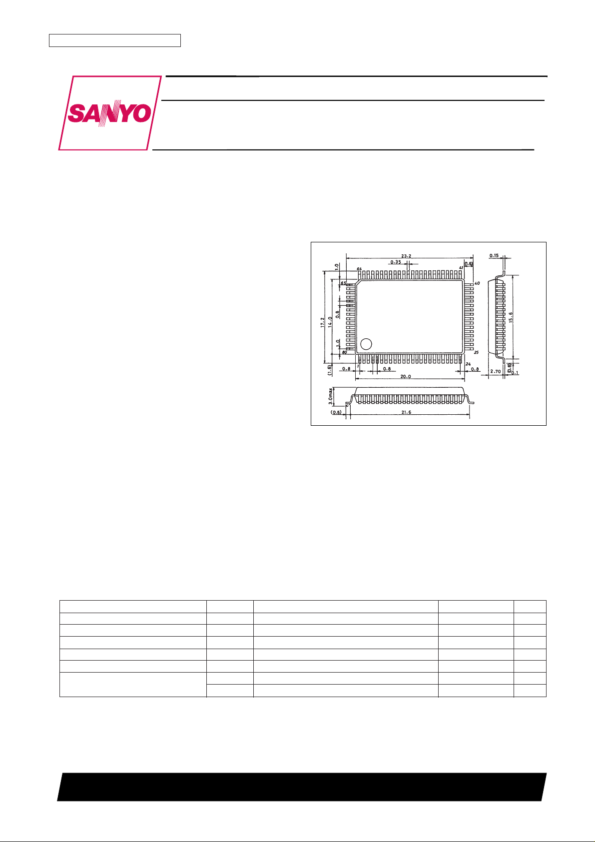
Package Dimensions
unit: mm
3174-QFP80E
CMOS LSI
Ordering number : EN *5753
93097HA (OT) No. 5753-1/5
Preliminary
SANYO Electric Co.,Ltd. Semiconductor Bussiness Headquarters
TOKYO OFFICE Tokyo Bldg., 1-10, 1 Chome, Ueno, Taito-ku, TOKYO, 110 JAPAN
Image Data Compression/Expansion Processor
LC8213K
Specifications
Absolute Maximum Ratings at Ta = 25°C, VSS= 0 V
Parameter Symbol Condition Ratings Unit
Maximum supply voltage V
DD
max –0.3 to +7.0 V
Input and output voltages V
I
, V
O
–0.3 to VDD+ 0.3 V
Allowable power dissipation Pd max Ta ≤ 70°C 500 mW
Operating temperature Topr –30 to +70 °C
Storage temperature Tstg –55 to +125 °C
Soldering conditions
Hand soldering: 3 seconds 350 °C
Reflow soldering: 10 seconds 235 °C
[LC8213K]
SANYO: QIP80E
Page 2
Allowable Operating Ranges at Ta = –30 to +70°C, VSS= 0 V
DC Characteristics at Ta = –30 to +70°C, VDD= 4.5 to 5.5 V
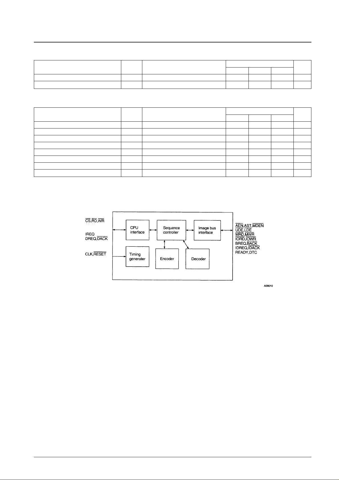
Block Diagram
• CPU interface
This circuit is a general-purpose 8-bit CPU interface. The operating mode and other aspects are set by accessing the
interface registers and the parameter registers.
• Sequence controller
Controls the functional blocks in the IC according to the encoding or decoding algorithm being used.
• Encoder
Generates the codes in the various modes by recognizing inflection points in the image data. Encoded data is passed to
the data bus through an 8-bit 4-word encoding FIFO (EFIFO).
• Decoder
Recognizes the codes in the various modes and recovers the original image data. Image data is passed to the data bus
through a decoding FIFO (DFIFO).
• Image bus interface
Controls reads from and writes to image memory as well as DMA transfers on the image memory bus.
No. 5753-2/5
LC8213K
Parameter Symbol Conditions
Ratings
Unit
min typ max
Supply voltage V
DD
4.5 5.0 5.5 V
Input voltage range V
IN
0 V
DD
V
Parameter Symbol Conditions
Ratings
Unit
min typ max
Input high-level voltage V
IH
1 2.2 V
Input low-level voltage V
IL
1 0.8 V
Input leakage current I
L
–10 +10 µA
Output high-level voltage V
OHIOH
= –4 mA 2.4 V
Output low-level voltage V
OLIOL
= 4 mA 0.4 V
Output leakage current I
OZ
For pins in the high-impedance output state –10 +10 µA
Input clock frequency f
CLK
CLK 25 MHz
Current drain I
DD
10 20 mA
A2 to A0
D7 to D0
TEST4 to TEST0
MA23 to MA16
MA/MD15 to MA/MD0
Page 3

Switching Characteristics at VDD= 2.7 to 5.5 V, Ta = –20 to +75°C, VSS= 0 V
I: Input pin O: Output pin B: Bi-directional pin P: Power supply pin NC: No connection
No. 5753-3/5
LC8213K
Pin No. Pin name I/O Function
1 CS I Chip select signal
2 RD I Read signal from the CPU
3 WR I Write signal from the CPU
4 A2 I
5 A1 I Address inputs
6 A0 I
7 V
DD
P Power supply
8 NC
9 D7 B
10 D6 B
Data bus
11 D5 B
12 D4 B
13 V
SS
P Ground
14 D3 B
15 D2 B
Data bus
16 D1 B
17 D0 B
18 NC
19 V
DD
P Power supply
20 IREQ O Interrupt request signal
21 DREQ O DMA request signal output to external DMA controller
22 DACK I DMA acknowledge signal input from external DMA controller
23 NC
24 NC
25 NC
26 NC
27 RESET I Reset signal input
28 CLK I Clock input
29 V
SS
P Ground
30 TEST4 I Test pin
31 V
DD
P Power supply
32 TEST3 I
33 TEST2 I
Test pin
34 TEST1 I
35 TEST0 I
36 NC
37 BREQ O Bus request signal for the image bus
38 BACK I Acknowledge signal for the image bus
39 IDREQ I DMA request signal from I/O devices
40 IDACK O DMA acknowledge signal to I/O devices
41 AEN O Address enable
42 AST O Address strobe
43 MDEN O Memory data enable
44 MRD O Image memory read signal
45 MWR O Image memory write signal
46 IORD O I/O device read signal
47 IOWR O I/O device write signal
48 LDE O Image bus lower byte valid signal
49 UDE O Image bus upper byte valid signal
50 READY I Ready signal
Continued on next page.
Page 4

Functional Description
• Encoding method
Conforms to the MH, MR, and MMR encoding methods of the ITU-T T.4 and T.6 recommendations, which are the
standards for G3 and G4 facsimile.
• Processing modes
Processing is performed in block units, and the number of lines processed can be set to be up to 64k lines. Processing can
also be performed in single line units. The LC8213K includes two FIFO systems, one for encoding and one for decoding,
so it is also possible to perform encoding and decoding alternately in units of several lines. In encoding mode, data is
read out sequentially from the image memory start address loaded into a register and encoded. The encoded data is
written to the encoding FIFO. The CPU is interrupted after the specified number of lines of data have been encoded. In
decoding mode, encoded data is read out of the decoding FIFO and decoded. The image data is recovered and written to
image memory. The CPU is interrupted after the specified number of lines of data have been decoded or a decoding error
occurs.
• Line skip mode
This is a mode in which the amount of code for a completely white line is set to half the set minimum number of
transmission bits. A line skip bit, which is used to recognize that a line is completely white, is added after the EOL code,
and fill bits are added so that the amount of code is one half the minimum number of transmission bits. For lines that are
not all white, the normal coded data is transmitted after the line skip bit.
No. 5753-4/5
LC8213K
Pin No. Pin name I/O Function
51 DTC O DMA transfer complete signal
52 V
SS
P Ground
53 V
DD
P Power supply
54 MA23 O
55 MA22 O
56 MA21 O
57 MA20 O
Upper 8 bits of the image memory address
58 MA19 O
59 MA18 O
60 MA17 O
61 MA16 O
62 MA/MD15 B Lower 16 bits of the image memory address/16-bit data bus
63 V
SS
P Ground
64 MA/MD14 B
65 MA/MD13 B
66 MA/MD12 B
67 MA/MD11 B
Lower 16 bits of the image memory address/16-bit data bus
68 MA/MD10 B
69 MA/MD9 B
70 MA/MD8 B
71 MA/MD7 B
72 V
SS
P Ground
73 V
DD
P Power supply
74 MA/MD6 B
75 MA/MD5 B
76 MA/MD4 B
77 MA/MD3 B Lower 16 bits of the image memory address/16-bit data bus
78 MA/MD2 B
79 MA/MD1 B
80 MA/MD0 B
Continued from preceding page.
Page 5

No. 5753-5/5
LC8213K
• CPU interface
The LC8213K has an 8-bit data bus. Various aspects of the operating mode can be set by accessing the interface
registers. Since the LC8213K provides interface pins for a DMA controller, DMA transfers with memory on the CPU
bus are supported.
• Image memory interface
The image memory has a 16-MB address space. A data bus width of either 8 or 16 bits can be selected.
• DMA transfer function
This function performs DMA transfers between image memory and I/O devices using the on-chip DMA controller. The
number of lines of data transferred can be set to any value up to 64k lines.
• Data transfers
Data can be transferred between the CPU bus and the image memory bus without encoding or decoding.
• Pad bit processing
Applications can select whether or not to perform pad bit processing. Pad bit processing consists of adding bits set to 0 at
the end of each line of encoded data so that the data for that line is an even multiple of 8 bits.
• Parameter settings
The LC8213K supports the following parameters, which can be set to any value in the indicated range.
• Number of bits processed on a single line (in byte units): 1 to 8k bytes
• Source document width (in byte units): 1 to 8k bytes
• Number of lines processed: 1 to 64k lines
• Minimum number of bits transmitted per line: 0 to 64k bits
• K parameter for MR encoding: 0 to 64k
• Number of lines handled in DMA transfers: 1 to 64k lines
• Number of EOL codes that form the RTC code: 0 to 255
Since the source document width and the number of bits processed on a single line can be set separately, the LC8213K
supports encoding or decoding the data for a subsection of the source document.
This catalog provides information as of September, 1997. Specifications and information herein are subject to
change without notice.
■ No products described or contained herein are intended for use in surgical implants, life-support systems, aerospace
equipment, nuclear power control systems, vehicles, disaster/crime-prevention equipment and the like, the failure of
which may directly or indirectly cause injury, death or property loss.
■ Anyone purchasing any products described or contained herein for an above-mentioned use shall:
➀ Accept full responsibility and indemnify and defend SANYO ELECTRIC CO., LTD., its affiliates, subsidiaries and
distributors and all their officers and employees, jointly and severally, against any and all claims and litigation and all
damages, cost and expenses associated with such use:
➁ Not impose any responsibility for any fault or negligence which may be cited in any such claim or litigation on
SANYO ELECTRIC CO., LTD., its affiliates, subsidiaries and distributors or any of their officers and employees
jointly or severally.
■ Information (including circuit diagrams and circuit parameters) herein is for example only; it is not guaranteed for
volume production. SANYO believes information herein is accurate and reliable, but no guarantees are made or implied
regarding its use or any infringements of intellectual property rights or other rights of third parties.
 Loading...