

Page 1

Ordering number: ENN*6585
64-Bit LED Driver for 300 dpi Printers
Preliminary
Overview
LC7958NC is a 64-bit constant current LED driver IC
designed to directly drive LED head array.
The output terminals for LED drive are arranged in
2-row staggered position of 80-µm pitch at one side. It
enables drive of LED Array of 300-dpi in one side
disposition, 600dpi in both sides disposition
Features and Functions
• Logic voltage ( VDD): +5 V ± 10 %
• LED drive current ( IOH): 5.0 mA (TYP)
• Clock frequency ( fc): 10 MHz
• Output current control circuit built in
• Mode switching function by the SEL pin
• Chip size: 1.43 mm × 5.39 mm
• Number of pads: 86
• 64-bit shift register circuit
• 64-bit latch circuit
• Output driver on/off switching function
• Constant current circuit
• 64-bit p-channel open drain LED driver
CMOS IC
LC7958NC
Any and all SANYO products described or contained herein do not have specifications that can handle
applications that require extremely high levels of reliability, such as life-support systems, aircraft's
control systems, or other applications whose failure can be reasonably expected to result in serious
physical and/or material damage. Consult with your SANYO representative nearest you before using
any SANYO products described or contained herein in such applications.
SANYO assumes no responsibility for equipment failures that result from using products at values that
exceed, even momentarily, rated values (such as maximum ratings, operating condition ranges, or other
parameters) listed in products specifications of any and all SANYO products described or contained
herein.
42800RM6585-1/11
Page 2

LC7958NC
The chara ct e ri st i cs s ho wn b e l o w a re th os e o f devi ce s e n c aps ul at e d in t he S ANYO s t a n dard c era m i c p a ckage
Specifications
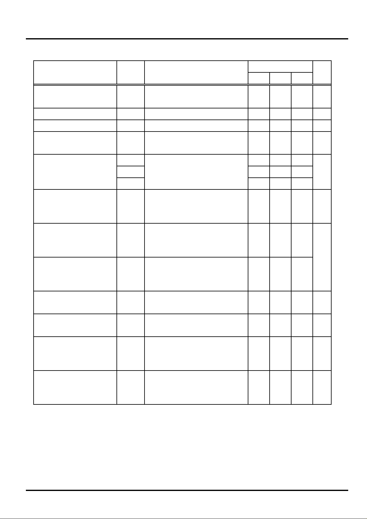
Absolute Maximum Ratings at Vss=0V
Parameter Symbol Conditions Ratings Unit
Power supply voltage
Input voltage VI Ta = 25 °C -0.3 to VDD1+ 0. 3 V
Output voltage VO Ta = 25 °C -0.3 to VDD1+ 0. 3 V
Driver output current IOUT 0 to -10 mA
Operating Junction temperature Tj -10 to 1 2 5 °C
Storage temperature Tstg -35 to 1 2 5 °C
VDD1 -0.3 to 6. 5
VDD2
Ta = 25 °C
-0.3 to 6. 5
Allowable Operating Ranges at Vss = 0 V, VDD1 = VDD2 = 5 V ± 10%, Ta = 0 to 100°C
Parameter Symbol Conditions
Power supply voltage
Potential difference*1 VDF
High-level input voltage VIH 2.0 VDD1 V
Low-level input voltage VIL
VDD1,VDD2
VDD1(pad 2),
VDD2(pad 6)
Between VDD1 a nd
VDD2
All inputs
Ratings
min typ max
4.5 5.5
-0.3 0 0.3
0 0.8 V
V
Unit
V
Clock frequency fc CLOCK 1 1 0 M Hz
Clock duty D CLK CLOCK 1 35 5 0 6 5 %
Setup time from SI to CLOCK1 tsc SI, CLOCK 1 3 0 ns
Hold time from CLOCK1 to S I thold SI, CLOCK 1 1 0 ns
Setup time from CLOCK1 to
LOAD1
Hold time from LOAD1 to CLOCK1 tHL LOAD 1, CLOCK 1 50 n s
LOAD1 pulse width tW L LOAD 1 40 ns
CLOCK1 rise/fall time
LOAD1 rise/fall time
*1:In case potential difference occurred between VDD1 and VDD2, Driver current value changes. Therefore using it with
VDD1=VDD2 is recommended.
tS L LOAD 1, CLOCK 1 5 0 ns
tCr
CLOCK 1 3 5 n s
tCf
tLr
LOAD 1 3 5 ns
tLf
6585-2/11
Page 3
LC7958NC
F
Electrical Characteristics at VSS = 0 V, VDD1 = VDD2 = 5 V ± 10%, Ta = 0 to 100°C
Parameter Symbol Conditions
min typ max
High-level output voltage VOH LOAD2, S0, CLOCK2: IO = -200µA
Low-level output voltage VOL LOAD2, S0, CLOCK2: IO = 2 00µA 0.5 V
Clock frequency fc 10 MHz
High-level input current IIH
IIL1 -1.0
IIL2 -8 -25 -50Low-level input current
IIL3
High-level output current IOH1
High-level output current
IOH2
minus correction
High-level output current
IOH3
plus correction
All input pads: VDD1 = 5.5 V, VI =
5.5 V
LOAD1, SI, CLOCK1, STROBE,
SEL, ADJ(-), ADJ(+): VDD1 = VDD2
= 5.5 V, VI = 0 V
DO1 to DO64: operation mode 1,
VDD1 = VDD2 = 5.0 V, VO = 1.6 V,
VREF = 1.8 V
DO1 to DO64: operation mode 2
VDD1 = VDD2 = 5.0 V, VO = 1.6 V,
VREF = 1.8 V
DO1 to DO64: operation mode 3
VDD1 = VDD2 = 5.0 V, VO = 1.6 V,
VREF = 1.8 V
VDD -
0.5
-40 -100 -200
-3.7 -5.0 -6.7 mA
-4.5 -6.0 -7.0
+4.5 +6.0 +7.0
Ratings
Unit
V
1.0 µA
µA
%
High-level output current
∆IOH DO1 to DO64: with all bits o n -5.0 +5.0 %
relative error between bits
Output off leakage current IO L
Operating current drain
IDD
(mode 1)
Standby current IDDS
DO1 to DO64: operation VDD1 =
5.5 V, VO = 0 V
VDD1: VDD1 = VDD2 = 5.5 V ,
VREF = 1.8 V, fc = 10 MHz, with
DO1 to DO64 o f f
VDD1: VDD1 = VDD2 = 5.5 V, VRE
= 1.8 V, with fc stopped, with DO1
to DO64 of f
0 -50 µA
9.0 13.0 m A
2.5 4.0 mA
6585-3/11
Page 4

LC7958NC
Switching Characteristics at VSS = 0 V, VDD1 = VDD2 = 5 V ± 10%, Ta = 0 to 100°C
Parameter Symbol Conditions
SO output rise time
SO output fall time t of
time from STROBE to DO
time from CLOCK2 to SO
CLOCK1→CLOCK2
transmission delay time tPL
tor
tpsrOutput transmission delay
tpsf
tpcrOutput transmission delay
tpcf
tPH
Eq uivalent Circui t Block Diagram
Constant
VREF
current
circuit
Ratings
Unit
min typ max
SO: CL=10.8pF 50 ns
STRO BE , DO1 to DO6 4: CL = 1 0.8
250 ns
pF, RF = 10 kΩ
CLOCK2, SO 1 0 7 0 ns
CLOC1, CLOCK2, LOAD1, LOAD2:
40 ns
CL=10.8 pF
DO64DO1
VDD2
64-bit constant current driver
VDD1
ADJ(+)
ADJ(-)
STROBE
SEL
LOAD1
SI
CLOCK1
64-bit latch
64-bit shift register
VSS
LOAD2
SO
CLOCK2
6585-4/11
Page 5

Sample Application Circuit Diagram
LC7958NC
GND
STROBE
VREF
VSS
VDD1
VDD2
(Input signal)
OPEN
SI
CLOCK1
LOAD1
VREF
SEL
STROBE
ADJ(-)
ADJ(+)
VSS
VDD 2
VDD1
LOAD2
CLOCK
SO
SI
CLOCK1
DO1
LED array
DO64
DO 1
LOAD1
VREF
SEL
STROB
ADJ(-)
ADJ(+)
VSS
VDD2
VDD1
LOAD
CLOCK
SO
DO64
LED array
(To the next input stage)
Note 1: The electric potential of the IC substrate is at VDD1.
Note 2: The number of cascade connection stages should b e within 60. (10MHz)
Note 3: All VDD2 terminals should be bonded.
Note 4: Leave the SEL Terminal of the odd-numbered IC open, and connect the SEL terminal of even-numbered IC with
VSS.
Note 5: Apply the stable potential other than the VDD1 and VDD2 lines to the VREF terminal.
6585-5/11
Page 6

Function Table
1. Shift Register and Latch Blocks
SEL CLOCK1 LOAD1 Shift register Latch
LC7958NC
Falling
edge
Rising edge - DATA keep -
High
- High - DATA load
- Low - DATA keep
Falling
edge
Rising edge - DATA keep -
Low
- Low - DATA load
- High - DATA keep
2. Output Block
STROBE SI DO output
-
-
DATA load and DATA
-
shift
DATA load and DATA
-
shift
High “×” OFF
Low Low OFF
Low High ON
Note 1: "×": don’t care
Establishment of Output Current
MODE ADJ(+) ADJ(-) Current control
resistance
1 Low Low Built in (RINT) VREF/RINT × 10
2 Low High Built in (RINT) VREF/RINT × 10 × 0.94
3 High Lo w Built in (RINT) VREF/RINT× 10 × 1.06
Note 2: RINT(TYP) = 3.61 kΩ
*Complement explanation
Here shows the general usage of the modes 1 to 3 as follows.
MODE 1 is set by connecting the ADJ(+) and ADJ(-) terminals with VSS. In the MODE1 state, by cutting the
bonding wire c onne c t e d with ADJ( + ) or ADJ( -) , the IC e nt e rs the MODE2 or MODE3, respe ctively. The c urrent i n
MODE1 ca n be c orrec te d by a bout –6 % or +6 % in MODE2 or MODE3, re spe c t ive l y.
IOH(typ)
6585-6/11
Page 7

LC7958NC
Ranking by Output Current
1. Test condition: VDD1 = VDD2 = 5.0 V, VREF = 1.8 V, VO = 1.6 V, T a = 25 °C
2. Ranking determination: The rank is determined by the average ON current (Iave) of the terminals DO1 to DO64 when
the all DO outputs are on.
3. Current width: (Imax - Imin)/(Imax + Imin) ≈ 2.0 %
Rank
ABC
- 1 - -3.700 to -3.853
- 2 - -3.854 to -4.011
- 3 - -4.012 to -4.177
1 4 - -4.178 to -4.347
2 5 - -4.348 to -4.524
3 6 - -4.525 to -4.708
4 7 1 -4.709 to -4.900
Specification [mA]
5 8 2 -4.901 to -5.100
6 9 3 -5.101 to -5.308
7 - 4 -5.309 to -5.524
8 - 5 -5.525 to -5.749
9 - 6 -5.750 to -5.983
- - 7 -5.984 to -6.227
- - 8 -6.228 to -6.481
- - 9 -6.482 to -6.700
* * * Rejected article (for the manufacturing process control)
Note: The chips of Ranking No. "*" are marked with the ink
ON Current Deviation in a Chip
Test condition: VDD1 = VDD2 = 5.0 V, VO = 1.6 V, VREF = 1.8 V, Ta = 25 °C
1. Let the average ON current of the terminals DO4, 12, 20, 28, 36, 44, 52, and 60 be Cave, the that of the terminals
DO1, 12, 20, and 28 be Lave, and that of the terminals DO36, 44, 52, and 60 be Rave: then the relationship among
the Cave, Lave, and Rave should be as follows.
| Lave - Cave | / Cave ≤ 2.5 % , | Rave - Cave | / Cave ≤ 2.5 %
2. Let the average ON current of DO1 to DO8, DO29 to DO36, and DO57 to DO64 be I1, I2, and I3, respectively: t he
relationship among the I1, I2, and I3 should be as follows.
| In - Iave | / Iave ≤ 2.5 %, Iave: Average ON current of the DO1 to DO64.
In: I2, and I3
6585-7/11
Page 8

Timing Chart (SEL = High)
CLOCK1
CLOCK2
ts c thold
SI
SO
LOAD1
LOAD2
LC7958NC
1/fc
tPL tPH
tpcr tpcf
tW
tSL tHL
tPH tPL
STROB
DOn(on)
DOn(off)
CLOCK1
LOAD1
tpsr tpsf
tCr tCf tor tof
90 %
SO
10 %
90 %
10 %
6585-8/11
Page 9

Pad Assignment
LC7958NC
85
86
16
22
15
21
20
X
23
24
Y
(0,0)
19
18
Chip size: 5.39 mm × 1.43 mm
Pad size: (PV open)
110 µm × 110 µm (Others)
2
17
1
Φ 110 µm (VDD2)
100 µm × 100 µm ( DOn)
Chip thickness: 330 µm ± 30 µm
6585-9/11
Page 10

LC7958NC
Pad Coordinates
No. Pin X Y No. Pin X Y
1 SI -2520 -484 44 DO22 -840 398
2 CLOCK1 -2040 -484 45 DO23 -760 539
3 LOAD1 -1800 -484 46 DO24 -680 398
4 VDD -1560 -484 47 DO25 -600 539
5 VREF -1080 -484 48 DO26 -520 398
6 SEL -840 -484 49 DO27 -440 539
7 STROBE -600 -484 50 DO28 -360 398
8 VSS -120 -484 51 DO29 -280 539
9 NC 120 -484 52 DO30 -200 398
10 ADJ(-) 600 -484 53 DO31 -120 539
11 ADJ(+) 840 -484 54 DO32 -40 398
12 VSS 1080 -484 55 DO33 40 539
13 VDD 1560 -484 56 DO34 120 398
14 LOAD2 1800 -484 57 DO35 200 539
15 CLOCK2 2040 -484 58 DO36 280 398
16 S0 2520 -484 59 DO37 360 539
17 VDD2 -2280 18 60 DO38 440 398
18 VDD2 -1320 18 61 DO39 520 539
19 VDD2 -360 18 62 DO40 600 398
20 VDD2 360 18 63 DO41 680 539
21 VDD2 1320 18 64 DO42 760 398
22 VDD2 2280 18 65 DO43 840 539
23 DO1 -2520 539 66 DO44 920 398
24 D02 -2440 398 67 DO45 1000 539
25 DO3 -2360 539 68 DO46 1080 398
26 DO4 -2280 398 69 DO47 1160 539
27 DO5 -2200 539 70 DO48 1240 398
28 DO6 -2120 398 71 DO49 1320 539
29 DO7 -2040 539 72 DO50 1400 398
30 DO8 -1960 398 73 DO51 1480 539
31 DO9 -1880 539 74 DO52 1560 398
32 DO10 -1800 398 75 DO53 1640 539
33 DO11 -1720 539 76 DO54 1720 398
34 DO12 -1640 398 77 DO55 1800 539
35 DO13 -1560 539 78 DO56 1880 398
36 DO14 -1480 398 79 DO57 1960 539
37 DO15 -1400 539 80 DO58 2040 398
38 DO16 -1320 398 81 DO59 2120 539
39 DO17 -1240 539 82 DO60 2200 398
40 DO18 -1160 398 83 DO61 2280 539
41 DO19 -1080 539 84 DO62 2360 398
42 DO20 -1000 398 85 DO63 2440 539
43 DO21 -920 539 86 DO64 2520 398
Unit: µm
6585-10/11
Page 11

LC7958NC
Specifications of any and all SANYO products described or contained herein stipulate the performance,
characteristics, and functions of the described products in the independent state, and are not guarantees
of the performance, characteristics, and functions of the described products as mounted in the customer's
products or equipment. To verify symptoms and states that cannot be evaluated in an independent device,
the customer should always evaluate and test devices mounted in the customer's products or equipment.
SANYO Electric Co., Ltd. strives to supply high-quality high-reliability products. However, any and all
semiconductor products fail with some probability. It is possible that these probabilistic failures could
give rise to accidents or events that could endanger human lives, that could give rise to smoke or fire,
or that could cause damage to other property. When designing equipment, adopt safety measures so
that these kinds of accidents or events cannot occur. Such measures include but are not limited to protective
circuits and error prevention circuits for safe design, redundant design, and structural design.
In the event that any or all SANYO products(including technical data,services) described or
contained herein are controlled under any of applicable local export control laws and regulations,
such products must not be exported without obtaining the export license from the authorities
concerned in accordance with the above law.
No part of this publication may be reproduced or transmitted in any form or by any means, electronic or
mechanical, including photocopying and recording, or any information storage or retrieval system,
or otherwise, without the prior written permission of SANYO Electric Co. , Ltd.
Any and all information described or contained herein are subject to change without notice due to
product/technology improvement, etc. When designing equipment, refer to the "Delivery Specification"
for the SANYO product that you intend to use.
Information (including circuit diagrams and circuit parameters) herein is for example only ; it is not
guaranteed for volume production. SANYO believes information herein is accurate and reliable, but
no guarantees are made or implied regarding its use or any infringements of intellectual property rights
or other rights of third parties.
This catalog provides information as of May, 2000. Specifications and information herein are subject to
change without notice.
PS
6585-11/11
 Loading...