

Page 1

CMOS LSI
Ordering number : EN4346B
73096HA (OT)/21593JN A8-9571 No. 4346-1/8
SANYO: MFP18
[LC73701M]
SANYO Electric Co.,Ltd. Semiconductor Bussiness Headquarters
TOKYO OFFICE Tokyo Bldg., 1-10, 1 Chome, Ueno, Taito-ku, TOKYO, 110 JAPAN
Dot Matrix LCD Driver
LC79400D
Overview
The LC79400D is a large-scale dot matrix LCD segment
driver LSI. Display data transferred from the controller
(4-bit parallel format) is processed through 80-bit
latching and a LCD drive signal is generated. The
LC79400D can be used in conjunction with common
driver LC7943D (QIP80D) as well as LC79430D
(QIP100D) and LC79431D (QIP100D) to drive a widescreen LCD panel.
Features
• On-chip LCD drive circuit (80 bits)
• Display duty selection ranging from 1/64 to 1/256
• Supports use of chip disable pin for lower large panel
power supply dissipation
• Supports externally supplied bias voltage
• Operating power supply voltage/operating temperature
include
VDD(logic block) : 5 V ±10 % / –20 to +75 °C
V
DD-VEE
(LCD block) :
12 V to 32 V / –20 to +75°C
• Data transfer clock provides maximum 3.0 MHz and
supports bidirectional shift
• 4-bit parallel data input
• CMOS process
• 100-pin flat plastic package
Package Dimensions
unit : mm
3180-QFP100D
Specifications
Absolute Maximum Ratings at Ta = 25±2°C, VSS= 0 V
Note:1. The voltages V1, V3, V4, V7, V
DD
and V
EE
must obey the relationships: VDD≥ V1 > V3 > V4 > VEE, VDD– V3 ≤ 7V,
V4 – VEE≤ 7V.
Parameter Symbol Conditions Ratings Unit
Maximum supply voltage (logic) V
DD
max –0.3 to +7.0 V
Maximum supply voltage (LCD) V
DD
- V
EE
max*
1
0 to 35 V
Maximum input voltage V
I
max –0.3 to VDD+ 0.3 V
Storage temperature range Tstg –40 to +125 °C
Page 2

LC79400D
No. 4346-2/8
Allowable Operating Ranges at Ta = –20 to +75°C, VSS= 0 V
Note:2. The voltages V1, V3, V4, V7, V
DD
and V
EE
must obey the relationships: VDD≥ V1 > V3 > V4 > VEE, VDD– V3 ≤ 7V, V4 – VEE≤
7V.
3. When applying
power,
apply
power to the LCD drive block after applying power to the logic block or apply power to both the blocks
simultaneously. When turning off power, turn off power to the logic block after turning off power to the LCD drive block or turn
off power to both the blocks simultaneously.
Electrical Characteristics at Ta = 25±2°C, VSS= 0 V, VDD= 5 V±10%
Note:4. VDE= V1 or V3 or V4 or VEE, V1 = VDD, V3 = 15/17 (VDD-VEE), V4 = 2/17 (VDD-VEE)
5. ISScurrent flows from VDDto VSS.
6. IEEcurrent flows from VDDto VEE.
Switching Characteristics at Ta = 25±2°C, VSS= 0 V, VDD= 5 V±10%
Parameter Symbol Conditions min typ max Unit
Supply voltage (logic) V
DD
4.5 5.5 V
Supply voltage (LCD) V
DD
- VEE*2, *
3
12 32 V
Input high-level voltage V
IH
DI1 to 4, CP, LOAD, CDR, CDL
0.8 V
DD
V
R/L, M, DISP OFF
Input low-level voltage V
IL
DI1 to 4, CP, LOAD, CDR, CDL
0.2 V
DD
V
R/L, M, DISP OFF
CP (shift clock) f
CP
CP 3.0 MHz
CP (pulse width) f
WC
CP 100 ns
LOAD pulse width t
WL
LOAD 100 ns
Setup time t
SETUP
DI1 to 4 → CP 80 ns
Hold time t
HOLD
DI1 to 4 → CP 80 ns
CP → LOAD
t
CL
1 CP → LOAD 0 ns
t
CL
2 CP → LOAD 100 ns
LOAD → CP t
LC
LOAD → CP 63 ns
t
R
CP 50 ns
Rise/Fall time
t
F
CP 50 ns
t
RL
LOAD 50 ns
t
FL
LOAD 50 ns
Parameter Symbol Conditions min typ max Unit
Input high-level current I
IH
VIN= VDD; LOAD, CP, CDR (CDL),
1 µA
R/L, DI1 to DI4, M, DISP OFF
Input low-level current I
IL
VIN= VSS; LOAD, CP, CDR (CDL),
–1 µA
R/L, DI1 to DI4, M, DISP OFF
Output high-level voltage V
OHIOH
= –400 µA; CDL (CDR) V
DD
– 0.4 V
Output low-level voltage V
OLIOL
= 400 µA; CDL (CDR) 0.4 V
R
ON
1
V
DD
– V
EE
= 30 V, V
DE
– VO = 0.5 V*4;
1.5 3.0 kΩ
Driver on resistor
O1 to O80
R
ON
2
V
DD
– V
EE
= 20 V, V
DE
– VO = 0.5 V*4;
2.0 3.5 kΩ
O1 to O80
Standby current dissipation I
ST
CDR (CDL) = VDD, V
DD
– V
EE
= 30 V
200
µA
CP = 3.0 MHz, no-load output: V
SS
I
SS
*
5
V
DD
– V
EE
= 30 V, CP = 3 MHz,
4.0 mA
Operation current dissipation
LOAD = 14 kHz, M = 35 Hz; V
SS
I
SS
*
6
V
DD
– V
EE
= 30 V, CP = 3 MHz,
0.1 mA
LOAD = 14 kHz, M = 35 Hz; V
EE
Input capacity C
I
f = 3.0 MHz; CP 5 pF
Parameter Symbol Conditions min typ max Unit
Output delay time t
D
Load = 15 pF; CDR (CDL) 200 ns
Page 3
LC79400D
No. 4346-3/8
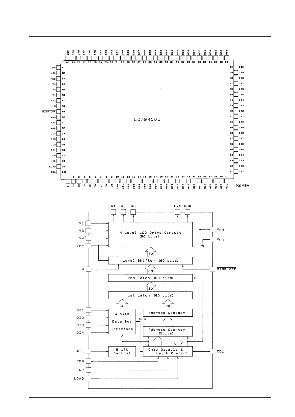
Pin Assignment
Equivalent Circuit Block Diagram
A00971
A00970
Page 4

Pin Descriptions
Pin No Pin name Input/Output Functions
90 V
DD
VDDand VSS: Power supply for logic section
92 V
SS
Power supply
83 V
EE
VDDand VEE: Power supply for LCD drive circuit
86 V1 LCD drive level power supply
85 V3 Power supply V1 and V
EE
: Select level
84 V4 V3 and V4 : Nonselect level
97 CP Input Display data shift clock (triggering on the trailing edge)
81 CDR Input/Output Chip disable pin
100 CDL Input/Output H level : Data not accepted
L level : Data accepted
99 LOAD Input
Display data latch clock (triggering on the trailing edge). On the trailing
edge, output levels switch in response to the particular combination of
display data, M and DISP OFF signals.
93 DI4 Input
94 DI3
95 DI2
96 DI1
88 M Input LCD drive output alternating signal
91 R/L Input
Input pin which performs input/output switching for CDR and CDL pins and
directional shift for 4-bit parallel input data.
1 O1 Output LCD drive output
2 O2
The combination of display data, M signal, and DISP OFF signal can be used
to create output levels as shown below.
79 O79
80 O80
89 DISP OFF Input
Input pin which controls output pins O1 to O80. V1 level is output from O1 to
O80 pin output during the low level input interval (See logic table).
R/L Input data and latch address
L
H
M Q DISP OFF Output
L L H V3
L H H V1
H L H V4
H H H V
EE
* * L V1
LC79400D
No. 4346-4/8
*Don’t care
(To be set to either "H" or "L")
Pin Name Input/Output R/L Pin Description
CDR Input L
Control input pin for the IC’s internal disable F/F
.
CDL Output
Output pin of the IC’s internal disable F/F.
Connects to the next stage CDR pin when
establishing a cascade connection.
CDL Input H
Control input pin for the IC’s internal disable F/F
.
CDR Output
Output pin of the IC’s internal disable F/F
.
Connects to the next stage CDL pin when
establishing a cascade connection.
Page 5

LC79400D
No. 4346-5/8
Operation Timing (for R/L = H)
A00974
Page 6

LC79400D
No. 4346-6/8
Time Chart (1/200 Duty 1/15 Bias)Switching Characteristics
A00975
Page 7

LC79400D
No. 4346-7/8
Sample Application
A00976
Page 8

No. 4346-8/8
LC79400D
This catalog provides information as of November, 1997. Specifications and information herein are subject to
change without notice.
■ No products described or contained herein are intended for use in surgical implants, life-support systems, aerospace
equipment, nuclear power control systems, vehicles, disaster/crime-prevention equipment and the like, the failure of
which may directly or indirectly cause injury, death or property loss.
■ Anyone purchasing any products described or contained herein for an above-mentioned use shall:
➀ Accept full responsibility and indemnify and defend SANYO ELECTRIC CO., LTD., its affiliates, subsidiaries and
distributors and all their officers and employees, jointly and severally, against any and all claims and litigation and all
damages, cost and expenses associated with such use:
➁ Not impose any responsibility for any fault or negligence which may be cited in any such claim or litigation on
SANYO ELECTRIC CO., LTD., its affiliates, subsidiaries and distributors or any of their officers and employees
jointly or severally.
■ Information (including circuit diagrams and circuit parameters) herein is for example only; it is not guaranteed for
volume production. SANYO believes information herein is accurate and reliable, but no guarantees are made or implied
regarding its use or any infringements of intellectual property rights or other rights of third parties.
Switching Characteristics
A00973
 Loading...