

Page 1

Ordering number : ENN7142
21202TN (OT) No. 7142-1/43
LC75816E, 75816W
SANYO Electric Co.,Ltd. Semiconductor Company
TOKYO OFFICE Tokyo Bldg., 1-10, 1 Chome, Ueno, Taito-ku, TOKYO, 110-8534 JAPAN
1/8 to 1/10 Duty Dot Matrix LCD Display Controllers/Drivers
with Key Input Function
CMOS IC
Any and all SANYO products described or contained herein do not have specifications that can handle
applications that require extremely high levels of reliability, such as life-support systems, aircraft’s
control systems, or other applications whose failure can be reasonably expected to result in serious
physical and/or material damage. Consult with your SANYO representative nearest you before using
any SANYO products described or contained herein in such applications.
SANYO assumes no responsibility for equipment failures that result from using products at values that
exceed, even momentarily, rated values (such as maximum ratings, operating condition ranges, or other
parameters) listed in products specifications of any and all SANYO products described or contained
herein.
• CCB is a trademark of SANYO ELECTRIC CO., LTD.
• CCB is SANYO’s original bus format and all the bus
addresses are controlled by SANYO.
Overview
The LC75816E and LC75816W are 1/8 to 1/10 duty dot
matrix LCD display controllers/drivers that support the
display of characters, numbers, and symbols. In addition to
generating dot matrix LCD drive signals based on data
transferred serially from a microcontroller, the LC75816E
and LC75816W also provide on-chip character display ROM
and RAM to allow display systems to be implemented easily.
These products also provide up to 2 general-purpose output
ports and incorporate a key scan circuit that accepts input
from up to 30 keys to reduce printed circuit board wiring.
Features
• Key input function for up to 30 keys (A key scan is
performed only when a key is pressed.)
• Controls and drives a 5 × 7, 5 × 8, or 5 ×9 dot matrix LCD.
• Supports accessory display segment drive (up to 65
segments)
• Display technique: 1/8 duty 1/4 bias drive (5 × 7 dots)
1/9 duty 1/4 bias drive (5 × 8 dots)
1/10 duty 1/4 bias drive (5 × 9 dots)
• Display digits: 13 digits × 1 line (5 × 7 dots)
12 digits × 1 line (5 × 8 dots, 5 × 9 dots)
• Display control memory
CGROM: 240 characters (5 × 7, 5 × 8, or 5 × 9 dots)
CGRAM: 16 characters (5 × 7, 5 × 8, or 5 × 9 dots)
ADRAM: 13 × 5 bits
DCRAM: 52 × 8 bits
• Instruction function
Display on/off control
Display shift function
• Sleep mode can be used to reduce current drain.
• Built-in display contrast adjustment circuit
• Switching between the key scan output port and generalpurpose output port functions can be controlled by
instructions.
• The frame frequency of the common and segment output
waveforms can be controlled by instructions.
• Serial data I/O supports CCB format communication
with the system controller.
• Independent LCD driver block power supply VLCD
• A voltage detection type reset circuit is provided to
initialize the IC and prevent incorrect display.
• The INH pin is provided. This pin turns off the display,
disables key scanning, and forces the general-purpose
output ports to the low level.
• RC oscillator circuit
Page 2
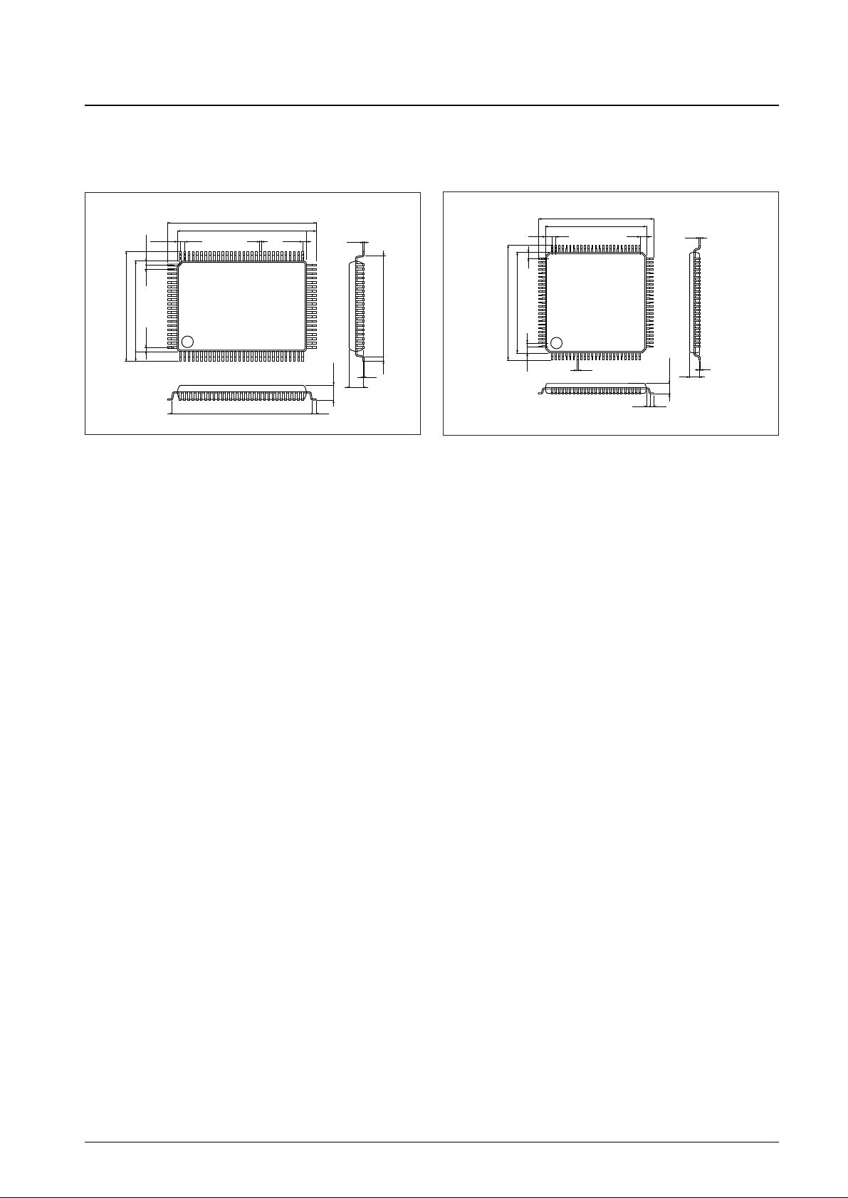
Package Dimensions
unit: mm
3151-QFP100E
unit: mm
3181B-SQFP100
No. 7142-2/43
LC75816E, 75816W
21.6
0.8
3.0max
1.6
17.2
0.825
1 30
31
50
51
80
81
1.6
0.575
0.575
0.15
2.7
15.6
0.3
20.0
23.2
14.0
0.65
0.825
100
0.8
0.65
0.1
SANYO: QFP100E
[LC75816E]
0.2
1.0
1.0
16.0
14.0
0.5
16.0
14.0
0.5
1.0
1.0
0.145
1.4
1.6max
0.5 0.5
100
1 25
26
50
5175
76
0.1
SANYO: SQFP100
[LC75816W]
Page 3

No. 7142-3/43
LC75816E, 75816W
Pin Assignments (Top View)
KS6
KI4
KI5
VLCD2
VSS
S4
S10
S16
S21
S15
S34
S39
S44
S59
S58
S49
S50
S51
S52
S53
S54
S55
S56
S57
S60
S61
S62
S63
S64/COM10
S65/COM9
COM8
COM7
COM6
COM5
COM4
COM3
COM2
COM1
KS1/P1
KS2/P2
KS3
KS4
KS5
S3S9S2
S1
DI
CL
KI1
LC75816E
(QFP100E)
KI2
KI3
VDD
VLCD
VLCD1
VLCD0
VLCD3
VLCD4
TEST
OSCO
INH
OSCI
DO
S33
S32
S31
S30
S29CE
5180
5081
31100
301
S8
S7
S6
S5
S14
S20
S13
S12
S11
S19
S18
S17
S25
S24
S23
S22
S28
S27
S26
S38
S37
S36
S35
S43
S42
S41
S40
S48
S47
S46
S45
S55
S51
S52
S53
S54
S56
S57
S58
S59
S60
S61
S62
S63
S64/COM10
S65/COM9
COM8
COM7
COM6
COM5
COM4
COM3
COM2
COM1
KS1/P1
KS2/P2
S5
S11
S4
S3
S2
S1
KS4
KS6
KS5
KI1
KS3
LC75816W
(SQFP100)
KI2
KI3
KI4
VDD
KI5
VLCD0
VLCD
VLCD1
VLCD3
VLCD2
VSS
VLCD4
TEST
OSCI
OSCO
INH
CE
DO
CL
S35
S34
S33
S32
S31
S29
S30
S27
S28
S26DI
5175
5076
26100
251
S10
S9
S8
S7
S6
S16
S22
S15
S14
S13
S12
S21
S20
S19
S18
S17
S25
S24
S23
S40
S39
S38
S37
S36
S45
S44
S43
S42
S41
S50
S49
S48
S47
S46
Page 4

No. 7142-4/43
LC75816E, 75816W
Parameter Symbol Conditions Ratings Unit
Maximum supply voltage
V
DD
max V
DD
–0.3 to +7.0
V
V
LCD
max V
LCD
–0.3 to +11.0
V
IN
1 CE, CL, DI, INH –0.3 to +7.0
Input voltage V
IN
2 OSCI, KI1 to KI5, TEST –0.3 to VDD+ 0.3 V
V
IN
3 V
LCD
1, V
LCD
2, V
LCD
3, V
LCD
4 –0.3 to V
LCD
+ 0.3
V
OUT
1 DO –0.3 to +7.0
Output voltage V
OUT
2 OSCO, KS1 to KS6, P1, P2 –0.3 to VDD+ 0.3 V
V
OUT
3 V
LCD
0, S1 to S65, COM1 to COM10 –0.3 to V
LCD
+ 0.3
I
OUT
1 S1 to S65 300 µA
Output current
I
OUT
2 COM1 to COM10 3
I
OUT
3 KS1 to KS6 1 mA
I
OUT
4 P1, P2 5
Allowable power dissipation Pd max Ta = 85°C 200 mW
Operating temperature Topr –40 to +85 °C
Storage temperature Tstg –55 to +125 °C
Specifications
Absolute Maximum Ratings at Ta = 25°C, VSS= 0 V
Parameter Symbol Conditions
Ratings
Unit
min typ max
V
DD
V
DD
4.5 6.0
Supply voltage
V
LCD
V
LCD
: When the display contrast adjustment circuit is used.
7.0 10.0 V
V
LCD
: When the display contrast adjustment circuit is not used.
4.5 10.0
Output voltage V
LCD
0 V
LCD
0 V
LCD
4+4.5 V
LCD
V
V
LCD
1 V
LCD
1
3/4 (V
LCD0–VLCD
4)
V
LCD
0
Input voltage
V
LCD
2 V
LCD
2
2/4 (V
LCD0–VLCD
4)
V
LCD
0
V
V
LCD
3 V
LCD
3
1/4 (V
LCD0–VLCD
4)
V
LCD
0
V
LCD
4 V
LCD
4 0 1.5
V
IH
1 CE, CL, DI, INH 0.8 V
DD
6.0
Input high level voltage V
IH
2 OSCI 0.7 V
DD
V
DD
V
V
IH
3 KI1 to KI5 0.6 V
DD
V
DD
Input low level voltage
V
IL
1 CE, CL, DI, INH, KI1 to KI5 0 0.2 V
DD
V
V
IL
2 OSCI 0 0.3 V
DD
Recommended external resistance R
OSC
OSCI, OSCO 33 kΩ
Recommended external capacitance C
OSC
OSCI, OSCO 220 pF
Guaranteed oscillation range f
OSC
OSC 150 300 600 kHz
Data setup time t
ds
CL, DI: Figure 2 160 ns
Data hold time t
dh
CL, DI: Figure 2 160 ns
CE wait time t
cp
CE, CL: Figure 2 160 ns
CE setup time t
cs
CE, CL: Figure 2 160 ns
CE hold time t
ch
CE, CL: Figure 2 160 ns
High level clock pulse width tøH CL: Figure 2 160 ns
Low level clock pulse width tøL CL: Figure 2 160 ns
DO output delay time t
dc
DO, RPU= 4.7kΩ, CL= 10pF*1: Figure 2 1.5 µs
DO rise time t
dr
DO, RPU= 4.7kΩ, CL= 10pF*1: Figure 2 1.5 µs
Allowable Operating Ranges at Ta = –40 to +85°C, VSS= 0 V
Note: *1. Since the DO pin is an open-drain output, these times depend on the values of the pull-up resistor RPUand the load capacitance CL.
Page 5
No. 7142-5/43
LC75816E, 75816W
Parameter Symbol Conditions
Ratings
Unit
min typ max
Hysteresis V
H
CE, CL, DI, INH, KI1 to KI5 0.1 V
DD
V
Power-down detection voltage V
DET
2.5 3.0 3.5 V
Input high level current I
IH
CE, CL, DI, INH, OSCI: VI= 6.0 V 5.0 µA
Input low level current I
IL
CE, CL, DI, INH, OSCI: VI= 0 V –5.0 µA
Input floating voltage V
IF
KI1 to KI5 0.05 V
DD
V
Pull-down resistance R
PD
KI1 to KI5: VDD= 5.0 V 50 100 250 kΩ
Output off leakage current I
OFFH
DO: VO= 6.0 V 6.0 µA
V
OH
1 S1 to S65: IO= –20 µA
V
LCD
0 – 0.6
VOH2 COM1 to COM10: IO= –100 µA
V
LCD
0 – 0.6
Output high level voltage VOH3 KS1 to KS6: IO= –500 µA VDD– 1.0
VDD– 0.5 VDD– 0.2
V
V
OH
4 P1, P2: IO= –1 mA VDD– 1.0
V
OH
5 OSCO: IO= –500 µA VDD– 1.0
V
OL
1 S1 to S65: IO= 20 µA
V
LCD
4 + 0.6
VOL2 COM1 to COM10: IO= 100 µA
V
LCD
4 + 0.6
Output low level voltage
V
OL
3 KS1 to KS6: IO= 25 µA 0.2 0.5 1.5
V
V
OL
4 P1, P2: IO= 1 mA 1.0
V
OL
5 OSCO: IO= 500 µA 1.0
V
OL
6 DO: IO= 1 mA 0.1 0.5
V
MID
1 S1 to S65: IO= ±20 µA
2/4 (V
LCD
0 – V
LCD
4) – 0.6 2/4 (V
LCD
0 – V
LCD
4) + 0.6
Output middle level voltage*
2
V
MID
2 COM1 to COM10: IO= ±100 µA
3/4 (V
LCD
0 – V
LCD
4) – 0.6 3/4 (V
LCD
0 – V
LCD
4) + 0.6
V
V
MID
3 COM1 to COM10: IO= ±100 µA
1/4 (V
LCD
0 – V
LCD
4) – 0.6 1/4 (V
LCD
0 – V
LCD
4) + 0.6
Oscillator frequency f
OSC
OSCI, OSCO: R
OSC
= 33 kΩ, C
OSC
= 220 pF 210 300 390 kHz
I
DD
1 VDD: sleep mode 100
I
DD
2 VDD: VDD= 6.0 V, output open, f
OSC
= 300 kHz 500 1000
Current drain
I
LCD
1 V
LCD
: sleep mode 5
µA
I
LCD
2
V
LCD
: V
LCD
= 10.0 V, output open, f
OSC
= 300 kHz 450 900
When the display contrast adjustment circuit is used.
I
LCD
3
V
LCD
: V
LCD
= 10.0 V, output open, f
OSC
= 300 kHz
200 400
When the display contrast adjustment circuit is not used.
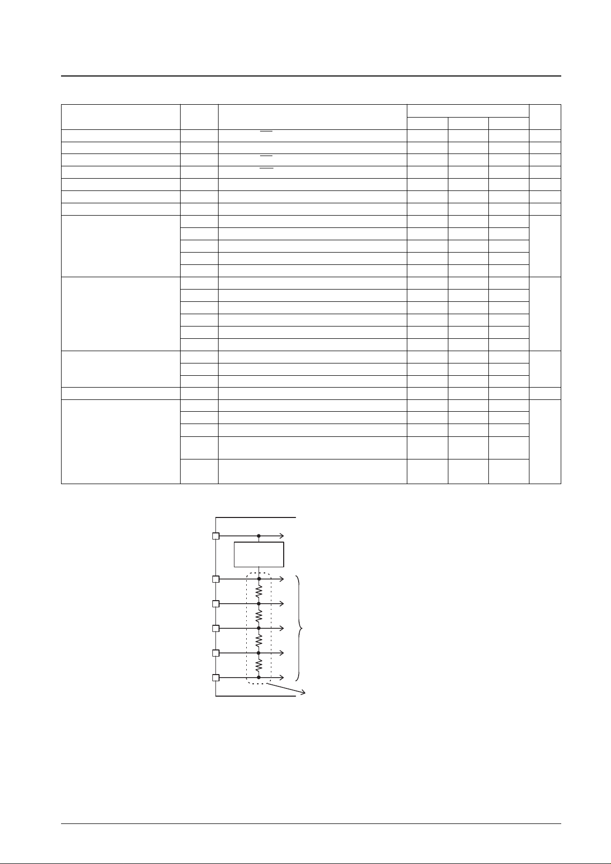
Electrical Characteristics for the Allowable Operating Ranges
Note: *2. Excluding the bias voltage generation divider resistor built into the V
LCD
0, V
LCD
1, V
LCD
2, V
LCD
3, and V
LCD
4. (See Figure 1.)
VLCD
VLCD3
VLCD4
VLCD2
VLCD0
VLCD1
CONTRAST
ADJUSTER
Excluding these resistors
To the common and segment drivers
Figure 1
Page 6

No. 7142-6/43
LC75816E, 75816W
• When CL is stopped at the low level
tdh
50%
VIH1
VIH1
VIL1
VIL1
VIH1
VIL1
tdr
tdc
tch
tcstcp
tds
CL
tøL
tøH
DO
DI
D1
D0
CE
• When CL is stopped at the high level
tøH
tøL
50%
VIH1
VIL1
tdh
VIH1
VIL1
VIH1
VIL1
tdr
tdc
tch
tcstcp
tds
CL
DO
DI
D1D0
CE
Block Diagram
S65/COM9
65
bits
CGRAM
5
× × × ×
×
9 16
bits
VDET
CLOCK
GENERATOR
CONTRAST
ADJUSTER
TIMING
GENERATOR
ADDRESS
REGISTER
INSTRUCTION
REGISTER
COMMON
DRIVER
INSTRUCTION
DECODER
ADDRESS
COUNTER
52 8
bits
CGROM
5 9 240
bits
S H I F T R E G I S T E R
L A T C H
S E G M E N T D R I V E R
OSCI
OSCO
INH
DO
DI
P1/KS1
P2/KS2
KS3
KS4
KS5
KS6
CE
KI1
KI2
KI3
KI4
KI5
CL
S1
S63
COM8
COM1
S64/COM10
KEY BUFFER
CCB INTERFACE
KEY SCAN
VDD
VLCD4
VLCD3
VLCD2
VLCD1
VLCD
VLCD0
VSS
TEST
Figure 2
ADRAM
DCRAM
Page 7

No. 7142-7/43
LC75816E, 75816W
Pin Functions
Pin
Pin No.
Function Active I/O Handling when unused
LC75816E LC75816W
Segment driver outputs.
The S64/COM10, S65/COM9 pins can be used as common
driver output under the “set display technique” instruction.
OPEN— O
S1 to S63
S64/COM10
S65/COM9
3 to 65
66
67
1 to 63
64
65
Common driver outputs. OPEN— OCOM1 to COM8 75 to 68 73 to 66
Oscillator connections. An oscillator circuit is formed by
connecting an external resistor and capacitor at these pins.
GND— IOSCI 97 95
Serial data interface connections to the controller. Note that DO,
being an open-drain output, requires a pull-up resistor.
CE : Chip enable
CL : Synchronization clock
DI : Transfer data
DO: Output data
GND
H ICE 100 98
ICL 1 99
— IDI 2 100
OPEN— OOSCO 96 94
Input that turns the display off, disables key scanning, and
forces the general-purpose output ports low.
• When INH is low (V
SS
):
• Display off
S1 to S63 = “L” (V
LCD
4).
S64/COM10, S65/COM9 = “L” (V
LCD
4).
COM1 to COM8 = “L” (V
LCD
4).
• General-purpose output ports P1, P2 = low (V
SS
)
• Key scanning disabled: KS1 to KS6 = low (V
SS
)
• All the key data is reset to low.
• When INH is high (V
DD
):
• Display on
• The state of the pins as key scan output pins or
general-purpose output ports can be set with the
"set key scan output port/general-purpose output
port state"
instruction
.
• Key scanning is enabled.
However, serial data can be transferred when the INH pin is low.
V
DD
L IINH 98 96
LCD drive 3/4 bias voltage (middle level) supply pin. This pin can
be used to supply the 3/4 (V
LCD
0 – V
LCD
4) voltage level externally.
OPEN— I
V
LCD
1
90 88
LCD drive 2/4 bias voltage (middle level) supply pin. This pin can
be used to supply the 2/4 (V
LCD
0 - V
LCD
4) voltage level externally.
OPEN— I
V
LCD
2
91 89
LCD drive 1/4 bias voltage (middle level) supply pin. This pin can
be used to supply the 1/4 (V
LCD
0 – V
LCD
4) voltage level externally.
OPEN— I
V
LCD
3
92 90
Logic block power supply connection. Provide a voltage of
between 4.5 and 6.0 V.
—— —
V
DD
87 85
LCD driver block power supply connection. Provide a voltage of
between 7.0 and 10.0 V when the display contrast adjustment
circuit is used and provide a voltage of between 4.5 and 10.0 V
when the circuit is not used.
—— —
V
LCD
88 86
Power supply connection. Connect to ground.
—— —
V
SS
94 92
Key scan outputs. Although normal key scan timing lines require
diodes to be inserted in the timing lines to prevent shorts, since
these outputs are unbalanced CMOS transistor outputs, these
outputs will not be damaged by shorting when these outputs are
used to form a key matrix. The KS1/P1 and KS2/P2 pins can be
used as general-purpose output ports under the "set key scan
output port/general-purpose output port state" instruction.
OPEN— O
KS1/P1
KS2/P2
KS3 to KS6
76
77
78 to 81
74
75
76 to 79
Key scan inputs.
These pins have built-in pull-down resistors.
GNDH IKI1 to KI5 82 to 86 80 to 84
DO 99 97 — O OPEN
This pin must be connected to ground. —— I
TEST
95 93
LCD drive 4/4 bias voltage (high level) supply pin. The level on
this pin can be changed by the display contrast adjustment circuit.
However, (V
LCD
0 – V
LCD
4) must be greater than or equal to 4.5
V. Also, external power must not be applied to this pin since the
pin circuit includes the display contrast adjustment circuit.
OPEN—
O
V
LCD
0
89 87
LCD drive 0/4 bias voltage (low level) supply pin. Fine
adjustment of the display contrast can be implemented by
connecting an external variable resistor to this pin.
However, (V
LCD
0 – V
LCD
4) must be greater than or equal to 4.5
V, and VLCD4 must be in the range 0 V to 1.5 V, inclusive.
GND— I
V
LCD
4
93 91
Page 8

No. 7142-8/43
LC75816E, 75816W
Block Functions
• AC (address counter)
AC is a counter that provides the addresses used for DCRAM and ADRAM.
The address is automatically modified internally, and the LCD display state is retained.
• DCRAM (data control RAM)
DCRAM is RAM that is used to store display data expressed as 8-bit character codes. (These character codes are
converted to 5 × 7, 5 × 8, or 5 × 9 dot matrix character patterns using CGROM or CGRAM.) DCRAM has a capacity of
52 × 8 bits, and can hold 52 characters. The table below lists the correspondence between the 6-bit DCRAM address
loaded into AC and the display position on the LCD panel.
•
When the DCRAM address loaded into AC is 00H.
Display digit 1 2 3 4 5 6 7 8 9 10 11 12 13
DCRAM address (hexadecimal) 00 01 02 03 04 05 06 07 08 09 0A 0B 0C
However, when the display shift is performed by specifying MDATA, the DCRAM address shifts as shown below.
Note: *3. The DCRAM address is expressed in hexadecimal.
Example: When the DCRAM address is 2EH.
Note: *4. 5 × 7 dots ... 13-digit display 5 × 7 dots
5 × 8 dots ... 13-digit display 4 × 8 dots
5 × 9 dots ... 13-digit display 3 × 9 dots
Display digit 1 2 3 4 5 6 7 8 9 10 11 12 13
DCRAM address (hexadecimal) 01 02 03 04 05 06 07 08 09 0A 0B 0C 0D
(Shift left)
Display digit 1 2 3 4 5 6 7 8 9 10 11 12 13
DCRAM address (hexadecimal) 33 00 01 02 03 04 05 06 07 08 09 0A 0B
DCRAM address DA0 DA1 DA2 DA3 DA4 DA5
(Shift right)
Least significant bit
↓
LSB
DA0 DA1 DA2 DA3 DA4 DA5
0 1 1 1 0 1
Most significant bit
↓
MSB
HexadecimalHexadecimal
Page 9

No. 7142-9/43
LC75816E, 75816W
• ADRAM (Additional data RAM)
ADRAM is RAM that is used to store the ADATA display data. ADRAM has a capacity of 13 × 5 bits, and the stored
display data is displayed directly without the use of CGROM or CGRAM. The table below lists the correspondence
between the 4-bit ADRAM address loaded into AC and the display position on the LCD panel.
•
When the ADRAM address loaded into AC is 0H. (Number of digit displayed: 13)
Display digit 1 2 3 4 5 6 7 8 9 10 11 12 13
ADRAM address (hexadecimal) 0 1 2 3 4 5 6 7 8 9 A B C
However, when the display shift is performed by specifying ADATA, the ADRAM address shifts as shown below.
Display digit 1 2 3 4 5 6 7 8 9 10 11 12 13
ADRAM address (hexadecimal) 1 2 3 4 5 6 7 8 9 A B C 0
(Shift left)
Display digit 1 2 3 4 5 6 7 8 9 10 11 12 13
ADRAM address (hexadecimal) C 0 1 2 3 4 5 6 7 8 9 A B
(Shift right)
Note: *5. The ADRAM address is expressed in hexadecimal.
Example: When the ADRAM address is A
H
Note: *6. 5 × 7 dots ... 13-digit display 5 dots
5 × 8 dots ... 13-digit display 4 dots
5 × 9 dots ... 13-digit display 3 dots
• CGROM (Character generator ROM)
CGROM is ROM that is used to generate the 240 kinds of 5 × 7, 5 × 8, or 5 × 9 dot matrix character patterns from the
8-bit character codes. CGROM has a capacity of 240 × 45 bits. When a character code is written to DCRAM, the
character pattern stored in CGROM corresponding to the character code is displayed at the position on the LCD
corresponding to the DCRAM address loaded into AC.
• CGRAM (Character generator RAM)
CGRAM is RAM to which user programs can freely write arbitrary character patterns. Up to 16 kinds of 5 × 7, 5 × 8,
or 5 × 9 dot matrix character patterns can be stored. CGRAM has a capacity of 16 × 45 bits.
ADRAM address RA0 RA1 RA2 RA3
RA0 RA1 RA2 RA3
0 1 0 1
Hexadecimal
Least significant bit
↓
LSB
Most significant bit
↓
MSB
Page 10

No. 7142-10/43
LC75816E, 75816W
Serial Data Input
• When CL is stopped at the low level
D63D62
D4D3D21 0000010 D0 D1
CE
CL
DI
DO
• When CL is stopped at the high level
•
B0 to B3, A0 to A3: CCB address 42H
•
D0 to D63: Instruction data
The data is acquired on the rising edge of the CL signal and latched on the falling edge of the CE signal. When
transferring instruction data from the microcontroller, applications must assure that the time from the transfer of one set
of instruction data until the next instruction data transfer is significantly longer than the instruction execution time.
D63D62
D4D3D20000 1010 D0 D1
CE
DI
DO
CL
Instruction data (Up to 64 bits)
Instruction data (Up to 64 bits)
A3A2A1A0B3B2B1B0
A3A2A1A0B3B2B1B0
Page 11
No. 7142-11/43
LC75816E, 75816W
Instruction Table
Notes: *7. The data format differs when the “DCRAM data write” instruction is executed in the increment mode (IM = 1).
(See detailed instruction descriptions .)
*8. The data format differs when the “ADRAM data write” instruction is executed in the increment mode (IM = 1).
(See detailed instruction descriptions.)
*9. The execution times listed here apply when fosc = 300 kHz. The execution times differ when the oscillator frequency fosc differs.
Example: When fosc = 210 kHz
300
27 µs ×—— = 39 µs
210
*10.When the sleep mode (SP = 1) is set, the execution time is 27 µs (when f
osc
= 300 kHz).
Instruction D0 D1...D39 D40 D41 D42 D43 D44 D45 D46 D47 D48 D49 D50 D51 D52 D53 D54 D55 Execution time *
9
Set display technique
Display on/off control DG1 DG2 DG3 DG4 DG5 DG6 DG7 DG8 DG9 DG10 DG11 DG12 DG13 X X X
Display shift
Set AC address DA0 DA1 DA2 DA3 DA4 DA5 X X
DCRAM data write *
7
AC0 AC1 AC2 AC3 AC4 AC5 AC6 AC7 DA0 DA1 DA2 DA3 DA4 DA5 X X
ADRAM data write *
8
AD1 AD2 AD3 AD4 AD5 X X X RA0 RA1 RA2 RA3 X X X X
CGRAM data write CD1 CD2...CD40 CD41 CD42 CD43 CD44 CD45 X X X CA0 CA1 CA2 CA3 CA4 CA5 CA6 CA7
Set display contrast CT0 CT1 CT2 CT3 X X X X
Set key scan output port/
KC1 KC2 KC3 KC4 KC5 KC6 X X
general-purpose output port state
D56 D57 D58 D59 D60 D61 D62 D63
DT1 DT2 FC X 0 0 0 1 0 µs
M A SC SP 0 0 1 0 0 µs/27 µs *
10
M A R/L X 0 0 1 1 27 µs
RA0 RA1 RA2 RA3 0 1 0 0 27 µs
IM X X X 0 1 0 1 27 µs
IM X X X 0 1 1 0 27 µs
X X X X 0 1 1 1 27 µs
CTC X X X 1 0 0 0 0 µs
PC1 PC2 KP1 KP2 1 0 0 1 0 µs
X: don’t care
Page 12

No. 7142-12/43
LC75816E, 75816W
Detailed Instruction Descriptions
• Set display technique ... <Sets the display technique>
Code
D56 D57 D58 D59 D60 D61 D62 D63
DT1 DT2 FC X 0 0 0 1
X: don’t care
X: don’t care
Note: *11 Sn (n = 64, 65): Segment outputs
COMn (n = 9, 10): Common outputs
DT1, DT2: Sets the display technique
DT1 DT2 Display technique
Output pins
S65/COM9 S64/COM10
0 0 1/8 duty, 1/4 bias drive S65 S64
1 0 1/9 duty, 1/4 bias drive COM9 S64
0 1 1/10 duty, 1/4 bias drive COM9 COM10
• Display on/off control ... <Turns the display on or off>
Code
D40 D41 D42 D43 D44 D45 D46 D47 D48 D49 D50 D51 D52 D53 D54 D55 D56 D57 D58 D59
DG1 DG2 DG3 DG4 DG5 DG6 DG7 DG8 DG9 DG10 DG11 DG12 DG13 X X X M A SC SP
D60 D61 D62 D63
0 0 1 0
M, A: Specifies the data to be turned on or off
Note: *12. MDATA, ADATA
5 × 7 dot matrix display 5 × 8 dot matrix display 5 × 9 dot matrix display
M A Display operating state
0 0 Both MDATA and ADATA are turned off (The display is forcibly turned off regardless of the DG1 to DG13 data.)
0 1 Only ADATA is turned on (The ADATA of display digits specified by the DG1 to DG13 data are turned on.)
1 0 Only MDATA is turned on (The MDATA of display digits specified by the DG1 to DG13 data are turned on.)
1 1 Both MDATA and ADATA are turned on (The MDATA and ADATA of display digits specified by the DG1 to DG13 data are turned on.)
DG1 to DG13: Specifies the display digit
For example, if DG1 to DG7 are 1, and DG8 to DG13 are 0, then display digits 1 to 7 will be turned on, and display digits 8
to 13 will be turned off (blanked).
Display digit 1 2 3 4 5 6 7 8 9 10 11 12 13
Display digit data DG1 DG2 DG3 DG4 DG5 DG6 DG7 DG8 DG9 DG10 DG11 DG12 DG13
FC: Sets the frame frequency of the common and segment output waveforms
FC
Frame frequency
1/8 duty, 1/4 bias drive f8 (Hz) 1/9 duty, 1/4 bias drive f9 (Hz) 1/10 duty, 1/4 bias drive f10 (Hz)
0
fosc fosc fosc
3072 3456 3840
1
fosc fosc fosc
1536 1728 1920
A10719
. . . .
. . .
ADATA
MDATA
. . . .
. . .
ADATA
MDATA
. . . .
. . .
MDATA
ADATA
Page 13
No. 7142-13/43
LC75816E, 75816W
SC: Controls the common and segment output pins
Note: *13. When SC is 1, the S1 to S65 and COM1 to COM10 output pins are set to the V
LCD
4 level, regardless of the M, A, and DG1 to DG13 data.
SC Common and segment output pin states
0 Output of LCD drive waveforms
1 Fixed at the V
LCD
4 level (all segments off)
SP: Controls the normal mode and sleep mode
SP Mode
0 Normal mode
Sleep mode
1
(The common and segment pins go to the V
LCD
4 level and the oscillator on the OSCI, OSCO pins is stopped (although it operates during key
scan operations), to reduce current drain. Although the "display on/off control", "set display contrast", and "set key scan output port/generalpurpose output port state"
instruction
s can be executed in this mode, applications must return the IC to normal mode to execute any of the other
instruction settings
.)
• Display shift ... <Shifts the display>
Code
D56 D57 D58 D59 D60 D61 D62 D63
M A R/L X 0 0 1 1
X: don’t care
M, A: Specifies the data to be shifted
M A Shift operating state
0 0 Neither MDATA nor ADATA is shifted
0 1 Only ADATA is shifted
1 0 Only MDATA is shifted
1 1 Both MDATA and ADATA are shifted
R/L: Specifies the shift direction
R/L Shift direction
0 Shift left
1 Shift right
X: don’t care
• Set AC address... <Specifies the DCRAM and ADRAM address for AC>
Code
D48 D49 D50 D51 D52 D53 D54 D55 D56 D57 D58 D59 D60 D61 D62 D63
DA0 DA1 DA2 DA3 DA4 DA5 X X RA0 RA1 RA2 RA3 0 1 0 0
DA0 to DA5: DCRAM address
DA0 DA1 DA2 DA3 DA4 DA5
LSB
↑
Least significant bit
MSB
↑
Most significant bit
RA0 to RA3: ADRAM address
RA0 RA1 RA2 RA3
LSB
↑
Least significant bit
MSB
↑
Most significant bit
This instruction loads the 6-bit DCRAM address DA0 to DA5 and the 4-bit ADRAM address RA0 to RA3 into the AC.
Page 14

No. 7142-14/43
LC75816E, 75816W
X: don’t care
• DCRAM data write ... <Specifies the DCRAM address and stores data at that address>
Code
D40 D41 D42 D43 D44 D45 D46 D47 D48 D49 D50 D51 D52 D53 D54 D55 D56 D57 D58 D59
AC0 AC1 AC2 AC3 AC4 AC5 AC6 AC7 DA0 DA1 DA2 DA3 DA4 DA5 X X IM X X X
D60 D61 D62 D63
0 1 0 1
DA0 to DA5: DCRAM address
DA0 DA1 DA2 DA3 DA4 DA5
AC0 to AC7: DCRAM data (character code)
This instruction writes the 8 bits of data AC0 to AC7 to DCRAM. This data is a character code, and is converted to a
5 × 7, 5 × 8, or 5 × 9 dot matrix display data using CGROM or CGRAM.
AC0 AC1 AC2 AC3 AC4 AC5 AC6 AC7
IM: Sets the method of writing data to DCRAM
Notes: *14.
· DCRAM data write method when IM = 0
IM DCRAM data write method
0 Normal DCRAM data write (Specifies the DCRAM address and writes the DCRAM data.)
1 Increment mode DCRAM data write (Increments the DCRAM address by +1 each time data is written to DCRAM.)
DCRAM data
write finishes
· DCRAM data write method when IM = 1 (Instructions other than the “DCRAM data write” instruction cannot be
executed.)
(1) (3)(2)(2)(2)(2)
DI
DCRAM
CE
CCB address CCB address
CCB address
CCB address
DCRAM data
write finishes
DCRAM data
write finishes
DCRAM data
write finishes
Instruction
execution time
Instruction
execution time
Instruction
execution time
Instruction
execution time
24 bits
24 bits
24 bits
24 bits
CCB address
CCB address
CCB address
CCB address
CCB address CCB address
24 bits
8 bits
8 bits
8 bits
8 bits
16 bits
Instruction
execution time
Instruction
execution
time
Instruction
execution
time
Instruction
execution time
Instruction
execution
time
Instruction
execution time
DCRAM data
write finishes
DCRAM data
write finishes
DCRAM data
write finishes
DCRAM data
write finishes
DCRAM data
write finishes
DCRAM data
write finishes
Instructions other than the “DCRAM data write” instruction cannot be executed.
LSB
↑
Least significant bit
LSB
↑
Least significant bit
MSB
↑
Most significant bit
MSB
↑
Most significant bit
CE
DI
(1) (1) (1) (1)
DCRAM
Page 15

No. 7142-15/43
LC75816E, 75816W
X: don’t care
Data format at (1) (24 bits)
Code
D40 D41 D42 D43 D44 D45 D46 D47 D48 D49 D50 D51 D52 D53 D54 D55 D56 D57 D58 D59
AC0 AC1 AC2 AC3 AC4 AC5 AC6 AC7 DA0 DA1 DA2 DA3 DA4 DA5 X X IM X X X
D60 D61 D62 D63
0 1 0 1
X: don’t care
• ADRAM data write ... <Specifies the ADRAM address and stores data at that address>
Code
D40 D41 D42 D43 D44 D45 D46 D47 D48 D49 D50 D51 D52 D53 D54 D55 D56 D57 D58 D59
AD1 AD2 AD3 AD4 AD5 X X X RA0 RA1 RA2 RA3 X X X X IM X X X
D60 D61 D62 D63
0 1 1 0
X: don’t care
Data format at (3) (16 bits)
Code
D48 D49 D50 D51 D52 D53 D54 D55 D56 D57 D58 D59 D60 D61 D62 D63
AC0 AC1 AC2 AC3 AC4 AC5 AC6 AC7 0 X X X 0 1 0 1
Data format at (2) (8 bits)
Code
D56 D57 D58 D59 D60 D61 D62 D63
AC0 AC1 AC2 AC3 AC4 AC5 AC6 AC7
RA0 to RA3: ADRAM address
AD1 to AD5: ADATA display data
In addition to the 5 × 7, 5 × 8, or 5 × 9 dot matrix display data (MDATA), this IC supports direct display of the five
accessory display segments provided in each digit as ADATA. This display function does not use CGROM or CGRAM.
The figure below shows the correspondence between the data and the display. When ADn = 1 (where n is an integer
between 1 and 5) the segment corresponding to that data will be turned on.
RA0 RA1 RA2 RA3
LSB
Least significant bit Most significant bit
MSB
ADATA Corresponding output pin
AD1 S5m + 1 (m is an integer between 0 and 12)
AD2 S5m + 2
AD3 S5m + 3
AD4 S5m + 4
AD5 S5m + 5
S5m+1
(m is an integer
S5m+5
between 0 and 12)
Page 16

No. 7142-16/43
LC75816E, 75816W
IM: Sets the method of writing data to ADRAM
IM ADRAM data write method
0 Normal ADRAM data write (Specifies the ADRAM address and writes the ADRAM data.)
1 Increment mode ADRAM data write (Increments the ADRAM address by +1 each time data is written to ADRAM.)
Notes: *15.
· ADRAM data write method when IM = 0
· ADRAM data write method when IM = 1 (Instructions other than the “ADRAM data write” instruction cannot
be excuted.)
X: don’t care
X: don’t care
Data format at (4) (24 bits)
Code
D40 D41 D42 D43 D44 D45 D46 D47 D48 D49 D50 D51 D52 D53 D54 D55 D56 D57 D58 D59
AD1 AD2 AD3 AD4 AD5 X X X RA0 RA1 RA2 RA3 X X X X IM X X X
D60 D61 D62 D63
0 1 1 0
X: don’t care
Data format at (6) (16 bits)
Code
D48 D49 D50 D51 D52 D53 D54 D55 D56 D57 D58 D59 D60 D61 D62 D63
AD1 AD2 AD3 AD4 AD5 X X X 0 X X X 0 1 1 0
Data format at (5) (8 bits)
Code
D56 D57 D58 D59 D60 D61 D62 D63
AD1 AD2 AD3 AD4 AD5 X X X
ADRAM data
write finishes
(4) (6)(5)(5)(5)(5)
DI
ADRAM
CE
CCB address
CCB address
CCB address
CCB address
ADRAM data
write finishes
ADRAM data
write finishes
ADRAM data
write finishes
Instruction
execution time
Instruction
execution time
Instruction
execution time
Instruction
execution time
24 bits
24 bits
24 bits
24 bits
CCB address
CCB address
CCB address
CCB address CCB address CCB address
24 bits
8 bits
8 bits
8 bits
8 bits
16 bits
Instruction
execution time
Instruction
execution
time
Instruction
execution
time
Instruction
execution time
Instruction
execution
time
Instruction
execution time
ADRAM data
write finishes
ADRAM data
write finishes
ADRAM data
write finishes
ADRAM data
write finishes
ADRAM data
write finishes
ADRAM data
write finishes
Instructions other than the “ADRAM data write” instruction cannot be excuted.
CE
DI
ADRAM
(4) (4) (4) (4)
Page 17

No. 7142-17/43
LC75816E, 75816W
X: don’t care
• CGRAM data write ... <Specifies the CGRAM address and stores data at that address>
Code
D0 D1 D2 D3 D4 D5 D6 D7 D8 D9 D10 D11 D12 D13 D14 D15
CD1 CD2 CD3 CD4 CD5 CD6 CD7 CD8 CD9 CD10 CD11 CD12 CD13 CD14 CD15 CD16
Code
D16 D17 D18 D19 D20 D21 D22 D23 D24 D25 D26 D27 D28 D29 D30 D31
CD17 CD18 CD19 CD20 CD21 CD22 CD23 CD24 CD25 CD26 CD27 CD28 CD29 CD30 CD31 CD32
Code
D32 D33 D34 D35 D36 D37 D38 D39 D40 D41 D42 D43 D44 D45 D46 D47
CD33 CD34 CD35 CD36 CD37 CD38 CD39 CD40 CD41 CD42 CD43 CD44 CD45 X X X
Code
D48 D49 D50 D51 D52 D53 D54 D55 D56 D57 D58 D59 D60 D61 D62 D63
CA0 CA1 CA2 CA3 CA4 CA5 CA6 CA7 X X X X 0 1 1 1
CA0 to CA7: CGRAM address
CD1 to CD45: CGRAM data (5 × 7, 5 × 8, or 5 × 9 dot matrix display data)
The bit CDn (where n is an integer between 1 and 45) corresponds to the 5 × 7, 5 × 8, or 5 × 9 dot matrix display data.
The figure below shows that correspondence. When CDn is 1 the dots which correspond to that data will be turned on.
Note: *16. CD1 to CD35: 5 × 7 dot matrix display data
CD1 to CD40: 5 × 8 dot matrix display data
CD1 to CD45: 5 × 9 dot matrix display data
CA0 CA1 CA2 CA3 CA4 CA5 CA6 CA7
CD1 CD2 CD3 CD4 CD5
CD6 CD7 CD8 CD9 CD10
CD11 CD12 CD13 CD14 CD15
CD16 CD17 CD18 CD19 CD20
CD21 CD22 CD23 CD24 CD25
CD26 CD27 CD28 CD29 CD30
CD31 CD32 CD33 CD34 CD35
CD36 CD37 CD38 CD39 CD40
CD41 CD42 CD43 CD44 CD45
LSB
↑
Least significant bit
MSB
↑
Most significant bit
Page 18

Note that although the display contrast can be adjusted by operating the built-in display contrast adjustment circuit, it is also
possible to apply fine adjustments to the contrast by connecting an external variable resistor to the V
LCD
4 pin and modifying
the V
LCD
4 pin voltage. However, the following conditions must be met: (V
LCD
0 – V
LCD
4) ≥ 4.5 V, and 1.5 V ≥ V
LCD
4 ≥ 0 V.
No. 7142-18/43
LC75816E, 75816W
• Set display contrast ... <Sets the display contrast>
X: don’t care
Code
D48 D49 D50 D51 D52 D53 D54 D55 D56 D57 D58 D59 D60 D61 D62 D63
CT0 CT1 CT2 CT3 X X X X CTC X X X 1 0 0 0
CT0 to CT3: Sets the display contrast (11 steps)
CT0 CT1 CT2 CT3 LCD drive 4/4 bias voltage supply V
LCD
0 level
0 0 0 0 0.94 V
LCD
= V
LCD
– (0.03 V
LCD
× 2)
1 0 0 0 0.91 V
LCD
= V
LCD
– (0.03 V
LCD
× 3)
0 1 0 0 0.88 V
LCD
= V
LCD
– (0.03 V
LCD
× 4)
1 1 0 0 0.85 V
LCD
= V
LCD
– (0.03 V
LCD
× 5)
0 0 1 0 0.82 V
LCD
= V
LCD
– (0.03 V
LCD
× 6)
1 0 1 0 0.79 V
LCD
= V
LCD
– (0.03 V
LCD
× 7)
0 1 1 0 0.76 V
LCD
= V
LCD
– (0.03 V
LCD
× 8)
1 1 1 0 0.73 V
LCD
= V
LCD
– (0.03 V
LCD
× 9)
0 0 0 1 0.70 V
LCD
= V
LCD
– (0.03 V
LCD
× 10)
1 0 0 1 0.67 V
LCD
= V
LCD
– (0.03 V
LCD
× 11)
0 1 0 1 0.64 V
LCD
= V
LCD
– (0.03 V
LCD
× 12)
CTC: Sets the display contrast adjustment circuit state
CTC Display contrast adjustment circuit state
0 The display contrast adjustment circuit is disabled, and the V
LCD
0 pin level is forced to the V
LCD
level.
1 The display contrast adjustment circuit operates, and the display contrast is adjusted.
Page 19

No. 7142-19/43
LC75816E, 75816W
• Set key scan output port/general-purpose output port state
... <Sets the key scan output port and general-purpose output port states>
X: don’t care
Code
D48 D49 D50 D51 D52 D53 D54 D55 D56 D57 D58 D59 D60 D61 D62 D63
KC1 KC2 KC3 KC4 KC5 KC6 X X PC1 PC2 KP1 KP2 1 0 0 1
KC1 to KC6: Sets the key scan output pin KS1 to KS6 state
Consider the case where the KS1/P1 and KS2/P2 output pins are set to function as key scan output ports. When KC1 to
KC3 are set to 1 and KC4 to KC6 are set to 0, in the key scan standby state the KS1 to KS3 output pins will output the
high level (VDD) and KS4 to KS6 will output the low level (VSS).
Note that key scan output signals are not output from output pins that are set to the low level.
Output pin KS1 KS2 KS3 KS4 KS5 KS6
Key scan output state setting data KC1 KC2 KC3 KC4 KC5 KC6
PC1, PC2: Sets the general-purpose output port P1, P2 state
Consider the case where the KS1/P1 and KS2/P2 output pins are set to function as general-purpose output ports. When
PC1 is set to 1 and PC2 is set to 0, the P1 output pin will output the high level (VDD) and P2 will output the low level
(VSS).
Output pin P1 P2
General-purpose output port state setting data PC1 PC2
Note: *17 KSn (n = 1, 2): Key scan output port
Pn (n = 1, 2): General-purpose output port
KP1, KP2: These bits switch the functions of the KS1/P1 and KS2/P2 output pins between the key scan output port and
the general-purpose output port.
KP1 KP2
Output pins
Maximum number of Number of general-
KS1/P1 KS2/P2
key inputs purpose output ports
0 0 KS1 KS2 30 0
1 0 P1 KS2 25 1
0 1 P1 P2 20 2
Page 20

No. 7142-20/43
LC75816E, 75816W
Serial Data Output
• When CL is stopped at the low level
CE
A3A2A1A0B3B2B1B0
KD2KD1X SA
KD30KD29KD28KD27
01000011
DO
DI
CL
X: don't care
Output data
• When CL is stopped at the high level
•
B0 to B3, A0 to A3 : CCB address 43H
•
KD1 to KD30 : Key data
•
SA : Sleep acknowledge data
Note: *18. If a key data read operation is executed when DO is high, the read key data (KD1 to KD30) and sleep
acknowledge data(SA) will be invalid.
Output data
X: don't care
CE
A3A2A1A0B3B2B1B0
KD3KD2KD1X XSA
KD30KD29KD28
01000011
DO
DI
CL
Page 21

No. 7142-21/43
LC75816E, 75816W
Output Data
• KD1 to KD30 : Key data
When a key matrix of up to 30 keys is formed from the KS1 to KS6 output pins and the KI1 to KI5 input pins and one
of those keys is pressed, the key output data corresponding to that key will be set to 1. The table shows the relationship
between those pins and the key data bits.
When the KS1/P1 and KS2/P2 output pins are set to function as general-purpose output ports with the "set key scan
output port/general-purpose output port state" instruction and a key matrix of up to 20 keys is formed from the KS3 to
KS6 output pins and the KI1 to KI5 input pins, the KD1 to KD10 key data bits will be set to 0.
• SA : Sleep acknowledge data
This output data bit is set to the state when the key was pressed. Also, while DO will be low in this case, if serial data is
input and the mode is set (to normal or sleep mode) during this period, that mode will be set. SA will be 1 in sleep
mode and 0 in normal mode.
KI1 KI2 KI3 KI4 KI5
KS1/P1 KD1 KD2 KD3 KD4 KD5
KS2/P2 KD6 KD7 KD8 KD9 KD10
KS3 KD11 KD12 KD13 KD14 KD15
KS4 KD16 KD17 KD18 KD19 KD20
KS5 KD21 KD22 KD23 KD24 KD25
KS6 KD26 KD27 KD28 KD29 KD30
Page 22

No. 7142-22/43
LC75816E, 75816W
• In normal mode
•
The pins KS1 to KS6 are set to high or low with the "set key scan output port/general-purpose output port state"
instruction.
•
If a key on one of the lines corresponding to a KS1 to KS6 pin which is set high is pressed, a key scan is started and
the keys are scanned until all keys are released. Multiple key presses are recognized by determining whether multiple
key data bits are set.
•
If a key is pressed for longer than 4800T(s) (Where T= ) the LC75816E/W outputs a key data read request (a
low level on DO) to the controller. The controller acknowledges this request and reads the key data. However, if CE
is high during a serial data transfer, DO will be set high.
•
After the controller reads the key data, the key data read request is cleared (DO is set high) and the LC75816E/W
performs another key scan. Also note that DO, being an open-drain output, requires a pull-up resistor (between 1 and
10 kΩ).
Key on
4608T[s]
*19
*19 *19
*19 *19
*19 *19
*19
*19
*19
*19
11
22
33
44
55
66
KS4
KS5
KS6
KS3
KS2
*19KS1
T =
1
fosc
DO
DI
Key address
(43H)
Key address Key address
CE
Key scan
Key data read request
Serial data
transfer
Serial data
transfer
Serial data
transfer
Key data read Key data read Key data read
Key data read request Key data read request
Key input 2
Key input 1
4800T[s] 4800T[s] 4800T[s]
T=
1
fosc
Note: *19. Not that the high/low states of these pins are determined by the "set key scan output port/general-purpose output port state"
instruction,
and that
key scan output signals are not output from pins that are set to low.
1
——
fosc
Key Scan Operation Functions
• Key scan timing
The key scan period is 2304T(s). To reliably determine the on/off state of the keys, the LC75816E/W scans the keys
twice and determines that a key has been pressed when the key data agrees. It outputs a key data read request (a low
level on DO) 4800T(s) after starting a key scan. If the key data dose not agree and a key was pressed at that point, it
scans the keys again. Thus the LC75816E/W cannot detect a key press shorter than 4800T(s).
Page 23

No. 7142-23/43
LC75816E, 75816W
• In sleep mode
•
The pins KS1 to KS6 are set to high or low with the "set key scan output port/general-purpose output port state"
instruction.
•
If a key on one of the lines corresponding to a KS1 to KS6 pin which is set high is pressed, the oscillator on the
OSCI, OSCO pins is started and a key scan is performed. Keys are scanned until all keys are released. Multiple key
presses are recognized by determining whether multiple key data bits are set.
•
If a key is pressed for longer than 4800T(s)(Where T= ) the LC75816E/W outputs a key data read request (a
low level on DO) to the controller. The controller acknowledges this request and reads the key data. However, if CE
is high during a serial data transfer, DO will be set high.
•
After the controller reads the key data, the key data read request is cleared (DO is set high) and the LC75816E/W
performs another key scan. However, this dose not clear sleep mode. Also note that DO, being an open-drain output,
requires a pull-up resistor (between 1 and 10 kΩ).
•
Sleep mode key scan example
Example: When a "display on/off control (SP = 1)" instruction and a "set key scan output port/general-purpose
output port state (KP1 and KP2 = 0, KC1 to KC5 = 0, KC6 = 1)" instruction are executed. (i.e. sleep mode with only
KS6 high.)
Multiple Key Presses
Although the LC75816E/W is capable of key scanning without inserting diodes for dual key presses, triple key presses on
the KI1 to KI5 input pin lines, or multiple key presses on the KS1 to KS6 output pin lines, multiple presses other than
these cases may result in keys that were not pressed recognized as having been pressed. Therefore, a diode must be
inserted in series with each key. Applications that do not recognize multiple key presses of three or more keys should
check the key data for three or more 1 bits and ignore such data.
KI1
KI2
KI3
KI4
KI5
*20
"L"KS3
"H"KS6
"L"KS2
When any one of these keys is pressed,
the oscillator on the OSCI, OSCO pins is
started and the keys are scanned.
"L"KS1
"L"KS4
"L"KS5
DO
DI
CE
Key input
(KS6 line)
Key scan
4800T[s] 4800T[s]
T =
1
fosc
Key address
(43H)
Key address
Serial data
transfer
Serial data
transfer
Serial data
transfer
Key data read Key data read
Key data read request Key data read request
1
——
fosc
Note: *20. These diodes are required to reliably recognize multiple key presses on the KS6 line when sleep mode state with only KS6 high, as in the above
example. That is, these diodes prevent incorrect operations due to sneak currents in the KS6 key scan output signal when keys on the KS1 to
KS5 lines are pressed at the same time.
Page 24

No. 7142-24/43
LC75816E, 75816W
1/8 Duty, 1/4 Bias Drive Technique
LCD driver output when all
LCD segments
corresponding to COM1 to
COM8 are turned on
VLCD3
VLCD4
VLCD4
VLCD2
VLCD1
VLCD0
VLCD4
VLCD3
VLCD3
VLCD2
VLCD2
VLCD1
VLCD1
VLCD0
VLCD0
COM8
COM2
COM1
VLCD4
VLCD3
VLCD2
VLCD1
VLCD0
VLCD4
VLCD3
VLCD2
VLCD1
VLCD0
VLCD4
VLCD3
VLCD2
VLCD1
VLCD0
T8
VLCD4
VLCD3
VLCD2
VLCD1
VLCD0
1
f8
T8 =
When a "set display technique" instruction with FC = 0 is executed: f8 =
When a "set display technique" instruction with FC = 1 is executed: f8 =
T8
8
fosc
3072
fosc
1536
LCD driver output when all
LCD segments
corresponding to COM1 to
COM8 are turned off
LCD driver output when
only LCD segments
corresponding to COM1
are turned on
LCD driver output when
only LCD segments
corresponding to COM2
are turned on
Page 25

No. 7142-25/43
LC75816E, 75816W
1/9 Duty, 1/4 Bias Drive Technique
VLCD3
VLCD4
VLCD4
VLCD2
VLCD1
VLCD0
VLCD4
VLCD3
VLCD3
VLCD2
VLCD2
VLCD1
VLCD1
VLCD0
VLCD0
COM9
COM2
COM1
VLCD4
VLCD3
VLCD2
VLCD1
VLCD0
VLCD4
VLCD3
VLCD2
VLCD1
VLCD0
VLCD4
VLCD3
VLCD2
VLCD1
VLCD0
VLCD4
VLCD3
VLCD2
VLCD1
VLCD0
T9
1
f9
T9 =
When a "set display technique" instruction with FC = 0 is executed: f9 =
When a "set display technique" instruction with FC = 1 is executed: f9 =
T9
9
fosc
3456
fosc
1728
LCD driver output when all
LCD segments
corresponding to COM1 to
COM9 are turned on
LCD driver output when all
LCD segments
corresponding to COM1 to
COM9 are turned off
LCD driver output when
only LCD segments
corresponding to COM1
are turned on
LCD driver output when
only LCD segments
corresponding to COM2
are turned on
Page 26

No. 7142-26/43
LC75816E, 75816W
1/10 Duty, 1/4 Bias Drive Technique
VLCD3
VLCD4
VLCD4
VLCD2
VLCD1
VLCD0
VLCD4
VLCD3
VLCD3
VLCD2
VLCD2
VLCD1
VLCD1
VLCD0
VLCD0
COM10
COM2
COM1
VLCD4
VLCD3
VLCD2
VLCD1
VLCD0
VLCD4
VLCD3
VLCD2
VLCD1
VLCD0
VLCD4
VLCD3
VLCD2
VLCD1
VLCD0
VLCD4
VLCD3
VLCD2
VLCD1
VLCD0
T10
1
f10
T10 =
When a "set display technique" instruction with FC = 0 is executed: f10 =
When a "set display technique" instruction with FC = 1 is executed: f10 =
T10
10
fosc
3840
fosc
1920
LCD driver output when all
LCD segments
corresponding to COM1 to
COM10 are turned on
LCD driver output when all
LCD segments
corresponding to COM1 to
COM10 are turned off
LCD driver output when
only LCD segments
corresponding to COM1
are turned on
LCD driver output when
only LCD segments
corresponding to COM2
are turned on
Page 27

No. 7142-27/43
LC75816E, 75816W
Voltage Detection Type Reset Circuit (VDET)
This circuit generates an output signal and resets the system when logic block power is first applied and when the voltage
drops, i.e., when the logic block power supply voltage is less than or equal to the power down detection voltage VDET,
which is 3.0V, typical. To assure that this function operates reliably, a capacitor must be added to the logic block power
supply line so that the logic block power supply voltage VDDrise time when the logic block power is first applied and the
logic block power supply voltage VDDfall time when the voltage drops are both at least 1 ms. (See Figure 3.)
Power Supply Sequence
The following sequences must be observed when power is turned on and off. (See Figure 3.)
• Power on :Logic block power supply(VDD) on → LCD driver block power supply(V
LCD
) on
• Power off:LCD driver block power supply(V
LCD
) off → Logic block power supply(VDD) off
However, if the logic and LCD driver blocks use a shared power supply, then the power supplies can be turned on and off
at the same time.
System Reset
1. Reset function
The LC75816E/W performs a system reset with the VDET. When a system reset is applied, the display is turned off, key
scanning is disabled, the key data is reset, and the general-purpose output ports are set to and held at the low level (VSS).
These states that are created as a result of the system reset can be cleared by executing the instruction described below.
(See Figure 3.)
• Clearing the display off state
Display operation can be enabled by executing a “display on/off control” instruction. However, since the contents of the
DCRAM, ADRAM, and CGRAM are undefined, applications must set the contents of these memories before turning on
display with the “display on/off control” instruction. That is, applications must execute the following instructions.
•
Set display technique
•
DCRAM data write
•
ADRAM data write (If the ADRAM is used.)
•
CGRAM data write (If the CGRAM is used.)
•
Set AC address
•
Set display contrast (If the display contrast adjustment circuit is used.)
After executing the above instructions, applications must turn on the display with a “display on/off control” instruction.
Note that when applications turn off in the normal mode, applications must turn off the display with a “display on/off
control” instruction or the INH pin.
• Clearing the key scan disable and key data reset states
Executing a "set key scan output port/general-purpose output port state" instruction not only creates a state in which
key scanning can be performed, but also clears the key data reset.
• Clearing the general-purpose output ports locked at the low level (VSS) state
Executing a "set key scan output port/general-purpose output port state" instruction clears the general-purpose output
ports locked at the low level (VSS) state and sets the states of the general-purpose output ports.
Page 28

No. 7142-28/43
LC75816E, 75816W
VDET
VDET
t1 t2
V
DD
V
LCD
Can be set to either the high (VDD), or low (VSS) level
Fixed at the low level (VSS)
• t1 ≥ 1 ms (Logic block power supply voltage VDDrise time)
• t2 ≥ 0 ms
• t3 ≥ 0 ms
• t4 ≥ 1 ms (Logic block power supply voltage VDDfall time)
• Initial state settings
Set display technique
DCRAM data write
ADRAM data write (If the ADRAM is used.)
CGRAM data write (If the CGRAM is used.)
Set AC address
Set display contrast (If the display contrast adjustment circuit is used.)
Instruction execution
Key scan
General-purpose
output ports
Display state
Initial state settings
Disabled
Execution enabled
Display off Display on
Display off
“Set key scan output
port/general-purpose output
port state” instruction execution
“Display on/off control”
instruction execution
(Turning the display on)
”Display on/off control“
instruction execution
(Turning the display off)
Figure 3
t3 t4
Page 29

No. 7142-29/43
LC75816E, 75816W
2. Block states during a system reset
(1) CLOCK GENERATOR, TIMING GENERATOR
When a reset is applied, the oscillator on the OSCI, OSCO pins is started forcibly. This generates the base clock and
enables instruction execution.
(2) INSTRUCTION REGISTER, INSTRUCTION DECODER
When a reset is applied, these circuits are forcibly initialized internally. Then, when instruction execution starts, the
IC operates according to those instructions.
(3) ADDRESS REGISTER, ADDRESS COUNTER
When a reset is applied, these circuits are forcibly initialized internally. Then, the DCRAM and the ADRAM
addresses are set when “Set AC address” instruction is executed.
(4) DCRAM, ADRAM, CGRAM
Since the contents of the DCRAM, ADRAM, and CGRAM become undefined during a reset, applications must
execute “DCRAM data write”, “ADRAM data write (If the ADRAM is used.)”, and “CGRAM data write (If the
CGRAM is used.)” instructions before executing a “display on/off control” instruction.
(5) CGROM
Character patterns are stored in this ROM.
(6) LATCH
Although the value of the data in the latch is undefined during a reset, the ADRAM, CGROM, and CGRAM data is
stored by executing a “display on/off control” instruction.
(7) COMMON DRIVER, SEGMENT DRIVER
These circuits are forced to the display off state when a reset is applied.
(8) CONTRAST ADJUSTER
Display contrast adjustment circuit operation is disabled when a reset is applied. After that, the display contrast can be
set by executing a “set display contrast” instruction.
(9) KEY SCAN, KEY BUFFER
When a reset is applied, these circuits are forcibly initialized internally, and key scan operation is disabled. Also, the
key data is all set to 0. After that, key scanning can be performed by executing a "set key scan output port/generalpurpose output port state" instruction.
(10) CCB INTERFACE, SHIFT REGISTER
These circuits go to the serial data input wait state.
Page 30

No. 7142-30/43
LC75816E, 75816W
S65/COM9
65
bits
5 9 16
bits
VDET
CLOCK
GENERATOR
CONTRAST
ADJUSTER
TIMING
GENERATOR
ADDRESS
REGISTER
INSTRUCTION
REGISTER
COMMON
DRIVER
INSTRUCTION
DECODER
ADDRESS
COUNTER
52 8
bits
CGROM
5 9 240
bits
S H I F T R E G I S T E R
L A T C H
S E G M E N T D R I V E R
OSCI
OSCO
INH
DO
DI
P1/KS1
P2/KS2
KS3
KS4
KS5
KS6
CE
KI1
KI2
KI3
KI4
KI5
CL
S1
S63
COM8
COM1
S64/COM10
KEY BUFFERCCB INTERFACE
KEY SCAN
VDD
VLCD4
VLCD3
VLCD2
VLCD1
VLCD
VLCD0
VSS
TEST
× ×
×
Blocks that are reset
3. Output pin states during the reset period
Notes: *21. These output pins are forcibly set to the segment output function and held at the low level (V
LCD
4). However, when a “set display technique”
instruction is executed, the segment output or the common output function is selected as specified by that instruction.
*22. These output pins are forcibly set to the general-purpose output port function and held at the low level (V
SS
). However, when a "set key scan
output port/general-purpose output port state" instruction has been executed, the key scan output port or general-purpose output port function will
be selected as specified by that instruction.
*23. Since this output pin is an open-drain output, a pull-up resistor (between 1 kΩ and 10 kΩ) is required. This pin is held at the high level even if a
key data read operation is performed before executing a "set key scan output port/general-purpose output port state" instruction.
Output pin State during reset
S1 to S63 L (V
LCD
4)
S64/COM10, S65/COM9 L (V
LCD
4)*
21
COM1 to COM8 L (V
LCD
4)
KS1/P1, KS2/P2 L (V
SS
)*
22
KS3 to KS6 L (VSS)
DO H *
23
ADRAM
CGRAM
× ×
DCRAM
Page 31

No. 7142-31/43
LC75816E, 75816W
Sample Application Circuit 1
1/8 duty, 1/4 bias drive technique (for use with normal panels)
COM9/S65
COM10/S64
S63
S62
S61
S10
S9
S8
S7
S6
S5
S4
S3
S2
S1
COM8
COM7
COM6
COM5
COM4
COM3
COM2
COM1
CCC
+8V
+5V
INH
CE
CL
DO
DI
OSCO
OSCI
VLCD4
VLCD3
VLCD2
VLCD1
OPEN
VLCD
VLCD0
VSS
TEST
VDD
K
S
1
K
/
2
P
/
1
P
S
2
K
S
3
K
S
4
K
S
5
K
S
6
K
I
1
K
I
2
K
I
3
K
I
4
K
I
5
Notes: *24. Add a capacitor to the logic block power supply line so that the logic block power supply voltage VDDrise time when power is applied and the
logic block power supply voltage V
DD
fall time when power drops are both at least 1 ms, as the LC75816E/W is reset by the VDET.
*25. If a variable resistor is not used for display contrast fine adjustment, the V
LCD
4 pin must be connected to ground.
*26. If the function of INH pin is not used, the INH pin must be connected to the logic block power supply V
DD
.
*27. The DO pin, being an open-drain output, requires a pull-up resistor. Select a resistance (between 1 to 10 kΩ) appropriate for the capacitance of
the external wiring so that signal waveforms are not degraded.
*24
*25
*26
C ≥ 0.047 µF
From the
controller
To the
controller
To the
controller
power supply
Key matrix
(up to 30 keys)
(general-purpose output ports)
used with the backlight controller
or other circuit
LCD panel
*27
Page 32

No. 7142-32/43
LC75816E, 75816W
Sample Application Circuit 2
1/8 duty, 1/4 bias drive technique (for use with large panels)
S63
S62
S61
S10
S9
S8
S7
S6
S5
S4
S3
S2
S1
COM8
COM7
COM6
COM5
COM4
COM3
COM2
COM1
R
R
R
R
CCC
+8V
+5V
INH
CE
CL
DO
DI
OSCO
OSCI
VLCD4
VLCD3
VLCD2
VLCD1
VLCD
VLCD0
VSS
TEST
VDD
K
S
1
K
S
2
K
S
3
K
S
4
K
S
5
K
S
6
K
I
1
K
I
2
K
I
3
K
I
4
K
I
5
COM9/S65
COM10/S64
/
2
P
/
1
P
*24
*25
*26
C ≥ 0.047 µF
10 kΩ ≥ R ≥ 2.2 kΩ
From the
controller
To the
controller
To the
controller
power supply
Key matrix
(up to 30 keys)
(general-purpose output ports)
used with the backlight controller
or other circuit
*27
LCD panel
Notes: *24. Add a capacitor to the logic block power supply line so that the logic block power supply voltage V
DD
rise time when power is applied and the
logic block power supply voltage V
DD
fall time when power drops are both at least 1 ms, as the LC75816E/W is reset by the VDET.
*25. If a variable resistor is not used for display contrast fine adjustment, the V
LCD
4 pin must be connected to ground.
*26. If the function of INH pin is not used, the INH pin must be connected to the logic block power supply V
DD
.
*27. The DO pin, being an open-drain output, requires a pull-up resistor. Select a resistance (between 1 to 10 kΩ) appropriate for the capacitance of
the external wiring so that signal waveforms are not degraded.
Page 33

No. 7142-33/43
LC75816E, 75816W
Sample Application Circuit 3
1/9 duty, 1/4 bias drive technique (for use with normal panels)
S63
S62
S61
S10
S9
S8
S7
S6
S5
S4
S3
S2
S65/COM9
S1
COM8
COM7
COM6
COM5
COM4
COM3
COM2
COM1
CCC
+8V
+5V
INH
CE
CL
DO
DI
OSCO
OSCI
VLCD4
VLCD3
VLCD2
VLCD1
OPEN
VLCD
VLCD0
VSS
TEST
VDD
K
S
1
K
S
2
K
S
3
K
S
4
K
S
5
K
S
6
K
I
1
K
I
2
K
I
3
K
I
4
K
I
5
COM10/S64
/
2
P
/
1
P
*24
*25
*26
C ≥ 0.047 µF
From the
controller
To the
controller
To the
controller
power supply
Key matrix
(up to 30 keys)
(general-purpose output ports)
used with the backlight controller
or other circuit
*27
LCD panel
Notes: *24. Add a capacitor to the logic block power supply line so that the logic block power supply voltage V
DD
rise time when power is applied and the
logic block power supply voltage V
DD
fall time when power drops are both at least 1 ms, as the LC75816E/W is reset by the VDET.
*25. If a variable resistor is not used for display contrast fine adjustment, the V
LCD
4 pin must be connected to ground.
*26. If the function of INH pin is not used, the INH pin must be connected to the logic block power supply V
DD
.
*27. The DO pin, being an open-drain output, requires a pull-up resistor. Select a resistance (between 1 to 10 kΩ) appropriate for the capacitance of
the external wiring so that signal waveforms are not degraded.
Page 34

No. 7142-34/43
LC75816E, 75816W
Sample Application Circuit 4
1/9 duty, 1/4 bias drive technique (for use with large panels)
S63
S62
S61
S10
S9
S8
S7
S6
S5
S4
S3
S2
S65/COM9
S1
COM8
COM7
COM6
COM5
COM4
COM3
COM2
COM1
R
R
R
R
CCC
+8V
+5V
INH
CE
CL
DO
DI
OSCO
OSCI
VLCD4
VLCD3
VLCD2
VLCD1
VLCD
VLCD0
VSS
TEST
VDD
K
S
1
K
S
2
K
S
3
K
S
4
K
S
5
K
S
6
K
I
1
K
I
2
K
I
3
K
I
4
K
I
5
COM10/S64
/
2
P
/
1
P
*24
*25
*26
From the
controller
To the
controller
To the
controller
power supply
Key matrix
(up to 30 keys)
(general-purpose output ports)
used with the backlight controller
or other circuit
*27
LCD panel
C ≥ 0.047 µF
10 kΩ ≥ R ≥ 2.2 kΩ
Notes: *24. Add a capacitor to the logic block power supply line so that the logic block power supply voltage VDDrise time when power is applied and the
logic block power supply voltage V
DD
fall time when power drops are both at least 1 ms, as the LC75816E/W is reset by the VDET.
*25. If a variable resistor is not used for display contrast fine adjustment, the V
LCD
4 pin must be connected to ground.
*26. If the function of INH pin is not used, the INH pin must be connected to the logic block power supply V
DD
.
*27. The DO pin, being an open-drain output, requires a pull-up resistor. Select a resistance (between 1 to 10 kΩ) appropriate for the capacitance of
the external wiring so that signal waveforms are not degraded.
Page 35

No. 7142-35/43
LC75816E, 75816W
Sample Application Circuit 5
1/10 duty, 1/4 bias drive technique (for use with normal panels)
S62
S61
S10
S9
S8
S7
S6
S5
S4
S3
S2
S64/COM10
S65/COM9
S1
COM8
COM7
COM6
COM5
COM4
COM3
COM2
COM1
CCC
+8V
+5V
INH
CE
CL
DO
DI
OSCO
OSCI
VLCD4
VLCD3
VLCD2
VLCD1
OPEN
VLCD
VLCD0
VSS
TEST
VDD
K
S
1
K
S
2
K
S
3
K
S
4
K
S
5
K
S
6
K
I
1
K
I
2
K
I
3
K
I
4
K
I
5
S63
/
2
P
/
1
P
*24
*25
*26
From the
controller
To the
controller
To the
controller
power supply
Key matrix
(up to 30 keys)
(general-purpose output ports)
used with the backlight controller
or other circuit
*27
LCD panel
C ≥ 0.047 µF
Notes: *24. Add a capacitor to the logic block power supply line so that the logic block power supply voltage V
DD
rise time when power is applied and the
logic block power supply voltage V
DD
fall time when power drops are both at least 1 ms, as the LC75816E/W is reset by the VDET.
*25. If a variable resistor is not used for display contrast fine adjustment, the V
LCD
4 pin must be connected to ground.
*26. If the function of INH pin is not used, the INH pin must be connected to the logic block power supply V
DD
.
*27. The DO pin, being an open-drain output, requires a pull-up resistor. Select a resistance (between 1 to 10 kΩ) appropriate for the capacitance of
the external wiring so that signal waveforms are not degraded.
Page 36

No. 7142-36/43
LC75816E, 75816W
Sample Application Circuit 6
1/10 duty, 1/4 bias drive technique (for use with large panels)
S63
S62
S61
S10
S9
S8
S7
S6
S5
S4
S3
S2
S64/COM10
S65/COM9
S1
COM8
COM7
COM6
COM5
COM4
COM3
COM2
COM1
R
R
R
R
CCC
+8V
+5V
INH
CE
CL
DO
DI
OSCO
OSCI
VLCD4
VLCD3
VLCD2
VLCD1
VLCD
VLCD0
VSS
TEST
VDD
K
S
1
K
S
2
K
S
3
K
S
4
K
S
5
K
S
6
K
I
1
K
I
2
K
I
3
K
I
4
K
I
5
/
2
P
/
1
P
*24
*25
*26
From the
controller
To the
controller
To the
controller
power supply
Key matrix
(up to 30 keys)
(general-purpose output ports)
used with the backlight controller
or other circuit
*27
LCD panel
C ≥ 0.047 µF
10 kΩ ≥ R ≥ 2.2 kΩ
Notes: *24. Add a capacitor to the logic block power supply line so that the logic block power supply voltage VDDrise time when power is applied and the
logic block power supply voltage V
DD
fall time when power drops are both at least 1 ms, as the LC75816E/W is reset by the VDET.
*25. If a variable resistor is not used for display contrast fine adjustment, the V
LCD
4 pin must be connected to ground.
*26. If the function of INH pin is not used, the INH pin must be connected to the logic block power supply V
DD
.
*27. The DO pin, being an open-drain output, requires a pull-up resistor. Select a resistance (between 1 to 10 kΩ) appropriate for the capacitance of
the external wiring so that signal waveforms are not degraded.
Page 37

No. 7142-37/43
LC75816E, 75816W
Sample Correspondence between Instructions and the Display (When the LC75816-8722 is used)
No.
LSB
Instruction (hexadecimal)
MSB
Display Operation
D40 to D43 D44 to D47 D48 to D51 D52 to D55 D56 to D59 D60 to D63
1
Power application Initializes the IC.
(Initialization with the VDET.) The display is in the off state.
2
Set display technique
Sets to 1/8 duty 1/4 bias display drive technique
0 8
3
DCRAM data write (increment mode)
Writes the display data “ ” to DCRAM address 00H
0 2 0 0 1 A
4
DCRAM data write (increment mode)
Writes the display data “S” to DCRAM address 01H
3 5
5
DCRAM data write (increment mode)
Writes the display data “A” to DCRAM address 02H
1 4
6
DCRAM data write (increment mode)
Writes the display data “N” to DCRAM address 03H
E 4
7
DCRAM data write (increment mode)
Writes the display data “Y” to DCRAM address 04H
9 5
8
DCRAM data write (increment mode)
Writes the display data “O” to DCRAM address 05H
F 4
9
DCRAM data write (increment mode)
Writes the display data “ ” to DCRAM address 06H
0 2
10
DCRAM data write (increment mode)
Writes the display data “L” to DCRAM address 07H
C 4
11
DCRAM data write (increment mode)
Writes the display data “S” to DCRAM address 08H
3 5
12
DCRAM data write (increment mode)
Writes the display data “I” to DCRAM address 09H
9 4
13
DCRAM data write (increment mode)
Writes the display data “ ” to DCRAM address 0AH
0 2
14
DCRAM data write (increment mode)
Writes the display data “L” to DCRAM address 0BH
C 4
15
DCRAM data write (increment mode)
Writes the display data “C” to DCRAM address 0CH
3 4
16
DCRAM data write (increment mode)
Writes the display data “7” to DCRAM address 0DH
7 3
17
DCRAM data write (increment mode)
Writes the display data “5” to DCRAM address 0EH
5 3
18
DCRAM data write (increment mode)
Writes the display data “8” to DCRAM address 0FH
8 3
19
DCRAM data write (increment mode)
Writes the display data “1” to DCRAM address 10H
1 3
20
DCRAM data write (increment mode)
Writes the display data “6” to DCRAM address 11H
6 3
21
DCRAM data write (increment mode)
Writes the display data “ ” to DCRAM address 12H
0 2 0 A
Continued on next page.
Page 38

No. 7142-38/43
LC75816E, 75816W
Continued from preceding page.
Note: *28. This sample above assumes the use of 13 digits 5 × 7 dot matrix LCD. CGRAM and ADRAM are not used.
X: don’t care
No.
LSB
Instruction (hexadecimal)
MSB
Display Operation
D40 to D43 D44 to D47 D48 to D51 D52 to D55 D56 to D59 D60 to D63
22
Set AC address Loads the DCRAM address 00H and the ADRAM
0 0 0 2 address 0H into AC
23
Display on/off control
Turns on the LCD for all digits (13 digits) in MDATA
F F F 1 1 4
24
Display shift
Shifts the display (MDATA only) to the left
1 C
25
Display shift
Shifts the display (MDATA only) to the left
1 C
26
Display shift
Shifts the display (MDATA only) to the left
1 C
27
Display shift
Shifts the display (MDATA only) to the left
1 C
28
Display shift
Shifts the display (MDATA only) to the left
1 C
29
Display shift
Shifts the display (MDATA only) to the left
1 C
30
Display on/off control
Set to sleep mode, turns off the LCD for all digits
0 0 0 0 8 4
31
Display on/off control
Turns on the LCD for all digits (13 digits) in MDATA
F F F 1 1 4
32
Set AC address Loads the DCRAM address 00H and the ADRAM
0 0 0 2 address 0H into AC
S A N Y O L S I L C
S A N Y O L S I L C 7
A N Y O L S I L C 7 5
N Y O L S I L C 7 5 8
Y O L S I L C 7 5 8 1
O L S I L C 7 5 8 1 6
L S I L C 7 5 8 1 6
L S I L C 7 5 8 1 6
S A N Y O L S I L C
Page 39

No. 7142-39/43
LC75816E, 75816W
Notes on the controller key data read techniques
1. Timer based key data acquisition
• Flowchart
• Timing chart
t5: Key scan execution time when the key data agreed for two key scans. (4800T(s))
t6: Key scan execution time when the key data did not agree for two key scans and the key scan was executed again. (9600T(s))
t7: Key address (43H) transfer time
t8: Key data read time
• Explanation
In this technique, the controller uses a timer to determine key on/off states and read the key data. The controller must
check the DO state when CE is low every t9 period without fail. If DO is low, the controller recognizes that a key has
been pressed and executes the key data read operation.
The period t9 in this technique must satisfy the following condition.
t9>t6+t7+t8
If a key data read operation is executed when DO is high, the read key data (KD1 to KD30) and sleep acknowledge
data (SA) will be invalid.
1
T = ———
fosc
YES
NO
DO = L
Key data read
processing
CE = L
DO
DI
CE
Key input
Key scan
Key onKey on
t6
t9t9t9t9
t5
t8 t8
t7
t7
t5
t7
t8
t5
Key address
Key data read
Key data read request
Controller
determination
(Key on)
Controller
determination
(Key on)
Controller
determination
(Key off)
Controller
determination
(Key on)
Controller
determination
(Key off)
Page 40

No. 7142-40/43
LC75816E, 75816W
2. Interrupt based key data acquisition
• Flowchart
• Timing chart
t5: Key scan execution time when the key data agreed for two key scans. (4800T(s))
t6: Key scan execution time when the key data did not agree for two key scans and the key scan was executed again. (9600T(s))
t7: Key address (43H) transfer time
t8: Key data read time
YES
YES
NO
DO = L
Key data read
processing
Wait for at least t10
CE = L
DO = H
CE = L
Key off
NO
DO
DI
CE
Key input
Key scan
Key onKey on
t10t10 t10t10
t5 t6
t8 t8
t7 t7
t5
t7
t8
t5
t7
t8
1
T = ———
fosc
Key address
Key data read
Controller
determination
(Key on)
Controller
determination
(Key off)
Controller
determination
(Key on)
Controller
determination
(Key on)
Controller
determination
(Key on)
Controller
determination
(Key off)
Key data read request
Page 41

No. 7142-41/43
LC75816E, 75816W
• Explanation
In this technique, the controller uses interrupts to determine key on/off states and read the key data. The controller
must check the DO state when CE is low. If DO is low, the controller recognizes that a key has been pressed and
executes the key data read operation. After that the next key on/off determination is performed after the time t10 has
elapsed by checking the DO state when CE is low and reading the key data. The period t10 in this technique must
satisfy the following condition.
t10 > t6
If a key data read operation is executed when DO is high, the read key data (KD1 to KD30) and sleep acknowledge
data (SA) will be invalid.
Page 42

No. 7142-42/43
LC75816E, 75816W
Upper
4bits
Lower
4bits
LC75816-8722 Character Font (Standard)
Page 43

PS No. 7142-43/43
LC75816E, 75816W
This catalog provides information as of February, 2002. Specifications and information herein are subject
to change without notice.
Specifications of any and all SANYO products described or contained herein stipulate the performance,
characteristics, and functions of the described products in the independent state, and are not guarantees
of the performance, characteristics, and functions of the described products as mounted in the customer’s
products or equipment. To verify symptoms and states that cannot be evaluated in an independent device,
the customer should always evaluate and test devices mounted in the customer’s products or equipment.
SANYO Electric Co., Ltd. strives to supply high-quality high-reliability products. However, any and all
semiconductor products fail with some probability. It is possible that these probabilistic failures could
give rise to accidents or events that could endanger human lives, that could give rise to smoke or fire,
or that could cause damage to other property. When designing equipment, adopt safety measures so
that these kinds of accidents or events cannot occur. Such measures include but are not limited to protective
circuits and error prevention circuits for safe design, redundant design, and structural design.
In the event that any or all SANYO products (including technical data, services) described or contained
herein are controlled under any of applicable local export control laws and regulations, such products must
not be exported without obtaining the export license from the authorities concerned in accordance with the
above law.
No part of this publication may be reproduced or transmitted in any form or by any means, electronic or
mechanical, including photocopying and recording, or any information storage or retrieval system,
or otherwise, without the prior written permission of SANYO Electric Co., Ltd.
Any and all information described or contained herein are subject to change without notice due to
product/technology improvement, etc. When designing equipment, refer to the “Delivery Specification”
for the SANYO product that you intend to use.
Information (including circuit diagrams and circuit parameters) herein is for example only; it is not
guaranteed for volume production. SANYO believes information herein is accurate and reliable, but
no guarantees are made or implied regarding its use or any infringements of intellectual property rights
or other rights of third parties.
 Loading...