

Page 1
Ordering number : EN3586A
SANYO Electric Co.,Ltd. Semiconductor Bussiness Headquarters
TOKYO OFFICE Tokyo Bldg., 1-10, 1 Chome, Ueno, Taito-ku, TOKYO, 110-8534 JAPAN
CMOS LSI
O2095HA (OT)/4032JN No. 3586-1/10
Overview
The LC7574NE and LC7574NW are 1/2 duty VFD
drivers that can be used for electronic tuning frequency
display and other applications under the control of a
controller. These products can directly drive VFDs with
up to 74 segments.
Features
• 74 segment outputs
• Noise reduction circuits are built into the output drivers.
• Serial data input supports CCB* format
communications with the system controller.
• Switching between digital and analog dimmers under
serial data control
• High generality since display data is displayed without
the intervention of a decoder
• All segments can be turned off with the BLK pin
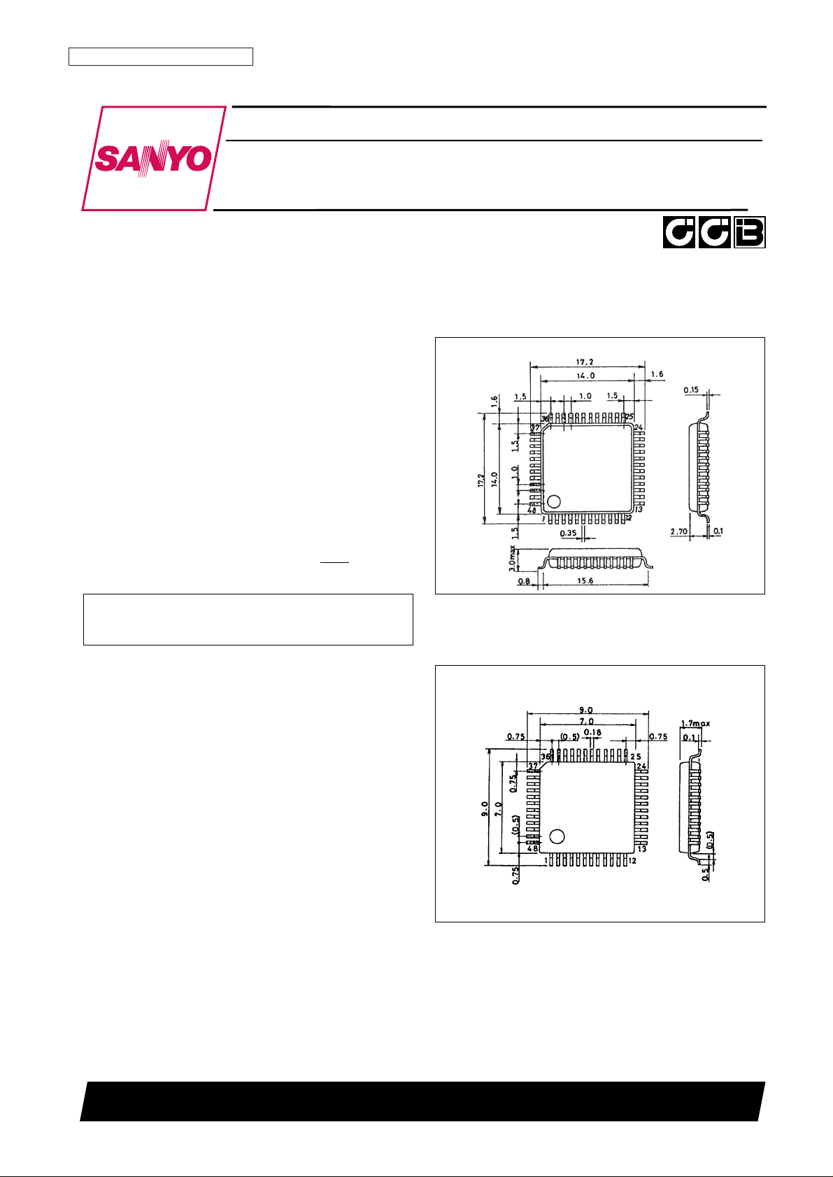
Package Dimensions
unit: mm
3156-QFP48E
SANYO: QFP48E
[LC7574NE]
unit: mm
3163A-SQFP48
SANYO: SQFP48
[LC7574NW]
• CCB is a trademark of SANYO ELECTRIC CO., LTD.
• CCB is SANYO’s original bus format and all the bus
addresses are controlled by SANYO.
1/2 Duty VFD Driver for Frequency Display
LC7574NE, 7574NW
Page 2

Specifications
Absolute Maximum Ratings at Ta = 25°C, VSS= 0 V
Allowable Operating Ranges at Ta = –40 to +85°C, VDD= 4.5 to 5.5 V, VSS= 0 V
Electrical Characteristics in the Allowable Operating Ranges
No. 3586-2/10
LC7574NE, 7574NW
Parameter Symbol Conditions Ratings Unit
Maximum supply voltage
V
DD
max V
DD
–0.3 to +6.5 V
V
FL
max V
FL
–0.3 to +21.0 V
Input voltage
V
IN
1 DI, CL, CE, BLK, DIM –0.3 to +6.5 V
V
IN
2 OSC –0.3 to VDD+ 0.3 V
Output voltage
V
OUT
1 S1 to S37, G1, G2 –0.3 to VFL+ 0.3 V
V
OUT
2 OSC –0.3 to VDD+ 0.3 V
Output current
I
OUT
1 S1 to S37 5 mA
I
OUT
2 G1, G2 67 mA
Allowable power dissipation Pd max
Ta = 85°C (LC7574NE) 250 mW
Ta = 85°C (LC7574NW) 150 mW
Operating temperature Topr –40 to +85 °C
Storage temperature Tstg –50 to +125 °C
Parameter Symbol Conditions min typ max Unit
Supply voltage
V
DD
V
DD
4.5 5.0 5.5 V
V
FL
V
FL
8 12 18 V
Input high level voltage V
IH
DI, CL, CE, BLK 0.8 V
DD
5.5 V
Input low level voltage V
IL
DI, CL, CE, BLK 0 0.2 V
DD
V
Guaranteed oscillator range f
OSC
OSC 0.4 1.6 3.0 MHz
Recommended external
R
OSC
OSC 12 kΩ
resistance
Recommended external
C
OSC
OSC 50 pF
capacitance
Low level clock pulse width t
øL
CL: Figure 1 0.5 µs
High level clock pulse width t
øH
CL: Figure 1 0.5 µs
Data setup time t
ds
DI, CL: Figure 1 0.5 µs
Data hold time t
dh
DI, CL: Figure 1 0.5 µs
CE wait time t
cp
CE, CL: Figure 1 0.5 µs
CE setup time t
cs
CE, CL: Figure 1 0.5 µs
CE hold time t
ch
CE, CL: Figure 1 0.5 µs
BLK switching time t
c
BLK, CE: Figure 3 10 µs
Input voltage range V
IN
DIM 0 +5.5 V
Parameter Symbol Conditions min typ max Unit
Input high level current I
IH
DI, CL, CE, BLK, DIM: VI= 5.5 V 5 µA
Input low level current I
IL
DI, CL, CE, BLK, DIM: VI= 0 V –5 µA
V
OH
1 S1 to S37: IO= 2 mA VFL– 0.6 V
Output high level voltage V
OH
2 G1, G2: IO= 25 mA VFL– 0.6 V
V
OH
3 G1, G2: IO= 50 mA VFL– 1.3 V
Output low level voltage V
OL
S1 to S37, G1, G2: IO= –5 µA, Ta = 25°C 0.125 0.25 0.5 V
Oscillator frequency f
OSC
R
OSC
= 12 kΩ, C
OSC
= 50 pF 1.6 MHz
Hysteresis voltage V
H
DI, CL, CE, BLK 0.5 V
A/D converter linearity error Err DIM –1/2 +1/2 LSB
Current drain I
DD
Outputs open: f
OSC
= 1.6 MHz 10 mA
Page 3

Pin Assignment
1. When CL is stopped at the low level
2. When CL is stopped at the high level
Figure 1
No. 3586-3/10
LC7574NE, 7574NW
Page 4

Block Diagram
Pin Functions
No. 3586-4/10
LC7574NE, 7574NW
Pin No. Pin I/O Function
Handling
when unused
4 V
FL
— Driver block power supply. A voltage of between 8.0 and 18.0 V must be supplied. —
1 V
DD
— Logic block power supply. A voltage of between 4.5 and 5.5 V must be supplied. —
46 V
SS
— Ground. Must be connected to the system ground. —
48 OSC I/O
Oscillator connection. An oscillator circuit is formed by connecting an external resistor and capacitor
to this pin
.
V
DD
Display off control input
47 BLK I
BLK = low (V
SS
): Display off (G1 and G2 = low)
GND
BLK = high (V
DD
): Display on
Note that serial data can be transferred while the display is turned off.
44 CL
Serial data transfer inputs. These pins must be
CL: synchronization clock
43 DI I
connected to the system controller.
DI: transfer data GND
42 CE
CE: chip enable
When the analog dimmer is selected, the analog voltage applied to this pin controls the duty of the G1
and G2 digit output pins. Since a 6-bit A/D converter is applied to this analog voltage and that result is
45 DIM I input to a decoder that provides a built-in dimmer curve, the relationship between the analog voltage GND
and the duty can be specified as a mask program. Note that 63/96 · VDDis the full-scale level for the
6-bit A/D converter.
2, 3 G1, G2 O Digit outputs. The frame frequency fOis (f
OSC
/4096) Hz Open
41 to 5 S1 to S37 O Segment outputs for displaying the display data transferred by serial data input. Open
Page 5

Serial Data Transfer Format
1. When CL is stopped at the low level
2. When CL is stopped at the high level
Figure 2
CCB address: Transfer 1010B, as shown in Figure 2.
M0: Digital/analog dimmer selection data
M0 = 0 ....................................Digital dimmer
M0 = 1 ....................................Analog dimmer
DM0 to DM9: Dimmer data
This data controls the duty of the G1 and G2 digit output pins when the digital dimmer is selected.
This data consists of 10 bits, of which DM0 is the LSB. Note that display intensity can be adjusted by
controlling the duty of the G1 and G2 digit output pins. (The DM0 to DM9 dimmer data is ignored
when the analog dimmer is selected.)
SD1 to SD74: Display data
SD1 to SD37...........................Display data for the G1 digit output pin
SD38 to SD74.........................Display data for the G2 digit output pin
SDn (n = 1 to 74) = 1..............Display on
SDn (n = 1 to 74) = 0..............Display off
T0: Test data
The T0 bit must be set to 0.
No. 3586-5/10
LC7574NE, 7574NW
Page 6

Serial Data Format
Correspondence between Display Data (SD1 to SD74) and Segment Output Pins
Example: Segment output pin S11 is controlled as follows:
No. 3586-6/10
LC7574NE, 7574NW
Segment output pin G1 G2
S1 SD1 SD38
S2 SD2 SD39
S3 SD3 SD40
S4 SD4 SD41
S5 SD5 SD42
S6 SD6 SD43
S7 SD7 SD44
S8 SD8 SD45
S9 SD9 SD46
S10 SD10 SD47
S11 SD11 SD48
S12 SD12 SD49
S13 SD13 SD50
S14 SD14 SD51
S15 SD15 SD52
S16 SD16 SD53
S17 SD17 SD54
S18 SD18 SD55
S19 SD19 SD56
Segment output pin G1 G2
S20 SD20 SD57
S21 SD21 SD58
S22 SD22 SD59
S23 SD23 SD60
S24 SD24 SD61
S25 SD25 SD62
S26 SD26 SD63
S27 SD27 SD64
S28 SD28 SD65
S29 SD29 SD66
S30 SD30 SD67
S31 SD31 SD68
S32 SD32 SD69
S33 SD33 SD70
S34 SD34 SD71
S35 SD35 SD72
S36 SD36 SD73
S37 SD37 SD74
Display data
Segment output pin S11 state
SD11 SD48
0 0 The segments corresponding to both the G1 and G2 digit output pins are off.
0 1 The segment corresponding to the G2 digit output pin is on.
1 0 The segment corresponding to the G1 digit output pin is on.
1 1 The segments corresponding to both the G1 and G2 digit output pins are on.
Page 7

BLK and the Display Control
Since the LSI internal data (SD1 to SD74 and the control data) is undefined when power is first applied, the display is
off (G1 and G2 = low) by setting the BLK pin low at the same time as power is applied. Then, meaningless display at
power on can be prevented by transferring all 92 bits of serial data from the controller while the display is off and setting
BLK pin high after the transfer completes. (See Figure 3.)
Power Supply Sequence
The following sequences must be observed when power is turned on and off. (See Figure 3)
• Power on: Logic block power supply (VDD) on → Driver block power supply (VFL) on
• Power off: Driver block power supply (VFL) off → Logic block power supply (VDD) off
Figure 3
Output Waveforms (S1 to S37)
No. 3586-7/10
LC7574NE, 7574NW
Page 8

Relation between Segment and Digit Outputs
Figure 4
Descriptions
1. Consider the examples shown in Figure 4, where data is set up so that the segment outputs S1 to S37 output a low
level on the G1 digit output timing and a high level on the G2 digit output timing. (Here, the G2 side being lighted)
2. The digit output G1 and G2 waveforms in Example 1 are output when the 10 bits of dimmer data (DM0 to DM9) are
set to 3FEH. The relation between t1 and the oscillator frequency f
OSC
is:
t1 = 2/f
OSC
.
For example, if f
OSC
= 1.6 [MHz], then
t1 = 2/1.6 [MHz] = 1.25 [µs].
Note that t1 and t2 are the same period in Example 1.
3. The digit output G1 and G2 waveforms in Example 2 are those when the dimmer data (DM0 to DM9) are set to a
smaller value. Although the time t1, which is from the point where digit output falls to segment output changes, does
not change, the time t2, which is from the point where segment output changes to the time the digit output rises,
becomes longer. When the dimmer data (DM0 to DM9) are set to 0FFHand f
OSC
is 1.6 [MHz], then the frame
frequency fOis:
fO= 1/(t3 × 2)
= f
OSC
/4096
= 391 [Hz],
and,
t3 = 1.28 [ms].
Therefore,
t2 = = 0.96 [ms].
4. When the dimmer data (DM0 to DM9) are set to an even smaller value, the time t2, which is from the point where
segment output changes to the time the digit output rises, becomes even longer, as in Example 3. Note that t1 does
not change here, either.
(1.28 [ms] – 1.25 [µs] × 2) × (3FFH– 0FFH)
1023
No. 3586-8/10
LC7574NE, 7574NW
Page 9

Sample Application Circuit
Usage Notes
1. Notes on the segment and digit waveforms
Figure 5
No. 3586-9/10
LC7574NE, 7574NW
Page 10

PS No. 3586-10/10
LC7574NE, 7574NW
The segment waveform is distorted by the VFD panel used and the wiring, and furthermore, in the case of being used
with essentially no dimming as in the digit waveform 1, as shown in Figure 5, the VFD panel glow dimly. By
carefully considering the segment waveform, it can be seen that this problem can be resolved by applying an
adequate amount of dimming, as shown in Digit waveform 2. When f
OSC
is 1.6 [MHz], we recommend using 10 bits
of dimmer data in the range 000H to 3E0H.
This catalog provides information as of October, 1995. Specifications and information herein are subject to
change without notice.
■ No products described or contained herein are intended for use in surgical implants, life-support systems, aerospace
equipment, nuclear power control systems, vehicles, disaster/crime-prevention equipment and the like, the failure of
which may directly or indirectly cause injury, death or property loss.
■ Anyone purchasing any products described or contained herein for an above-mentioned use shall:
➀ Accept full responsibility and indemnify and defend SANYO ELECTRIC CO., LTD., its affiliates, subsidiaries and
distributors and all their officers and employees, jointly and severally, against any and all claims and litigation and all
damages, cost and expenses associated with such use:
➁ Not impose any responsibility for any fault or negligence which may be cited in any such claim or litigation on
SANYO ELECTRIC CO., LTD., its affiliates, subsidiaries and distributors or any of their officers and employees
jointly or severally.
■ Information (including circuit diagrams and circuit parameters) herein is for example only; it is not guaranteed for
volume production. SANYO believes information herein is accurate and reliable, but no guarantees are made or implied
regarding its use or any infringements of intellectual property rights or other rights of third parties.
 Loading...