

Page 1
Overview
The LC75725E is a 1/4 to 1/11 duty dynamic drive VFD
driver. It provides 43 segment outputs and 11 digit
outputs. It facilitates the construction of display systems
operating under the control of a controller.
Features
• Dynamic drive display technique to display four to
eleven digits on the VFD.
• Serial data input supports CCB* format communication
with the system controller.
• The dimmer level is controlled by serial data input.
(The dimmer has a resolution of 10 bits.)
• High generality since display data is displayed without
the intervention of a decoder.
• All segments can be turned off with the BLK pin.
• CR oscillator circuit.
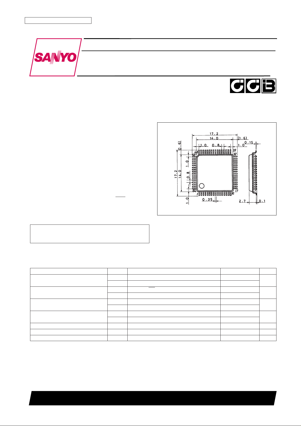
Package Dimensions
unit: mm
3159-QFP64E
CMOS LSI
Ordering number : EN5606
3398HA (OT) No. 5606-1/13
SANYO Electric Co.,Ltd. Semiconductor Bussiness Headquarters
TOKYO OFFICE Tokyo Bldg., 1-10, 1 Chome, Ueno, Taito-ku, TOKYO, 110-8534 JAPAN
1/4 to 1/11 Duty Dynamic Drive VFD Driver
LC75725E
SANYO: QIP64E
[LC75725E]
• CCB is a trademark of SANYO ELECTRIC CO., LTD.
• CCB is SANYO’s original bus format and all the bus
addresses are controlled by SANYO.
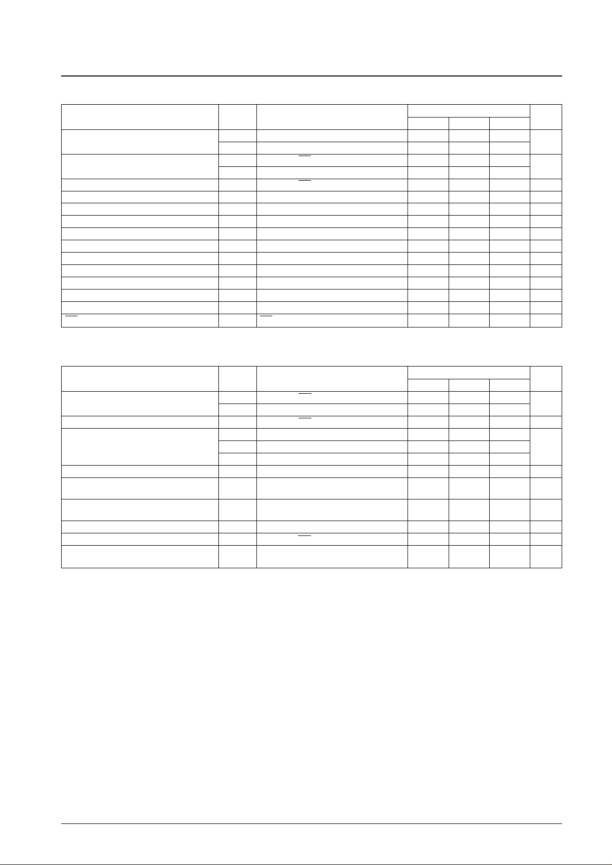
Parameter Symbol Conditions Ratings Unit
Maximum supply voltage
V
DD
max V
DD
–0.3 to +6.5
V
V
FL
max V
FL
VDD– 47 to VDD+0.3
Input voltage
V
IN
1 DI, CL, CE, BLK –0.3 to +6.5
V
V
IN
2 OSCI –0.3 to V
DD
+0.3
Output voltage
V
OUT
1 S1 to S43, G1 to G11 V
DD
– 47 to VDD+0.3
V
V
OUT
2 OSCO –0.3 to V
DD
+0.3
Output current
I
OUT
1 S1 to S43 10
mA
I
OUT
2 G1 to G11 30
Allowable power dissipation Pd max Ta = 85°C 300 mW
Operating temperature Topr –40 to +85 °C
Storage temperature Tstg –50 to +150 °C
Specifications
Absolute Maximum Ratings at Ta = 25°C, VSS= 0 V
Page 2
No. 5606-2/13
LC75725E
Parameter Symbol Conditions
Ratings
Unit
min typ max
Supply voltage
V
DDVDD
4.5 5.0 5.5
V
V
FL
V
FL
VDD– 45 V
DD
Input high-level voltage
V
IH
1 DI, CL, CE, BLK 0.8 V
DD
5.5
V
V
IH
2 OSCI 0.8 V
DD
V
DD
Input low-level voltage V
IL
DI, CL, CE, BLK, OSCI 0 0.2 V
DD
V
Guaranteed oscillator range f
OSC
OSCI, OSCO 1.8 3.7 4.9 MHz
Recommended external resistance R
OSC
OSCI, OSCO 1.0 5.6 22 KΩ
Recommended external capacitance C
OSC
OSCI, OSCO 10 22 47 pF
Low level clock pulse width t
øL
CL Figure 1 0.5 µs
High level clock pulse width t
øH
CL Figure 1 0.5 µs
Data setup time t
ds
DI, CL Figure 1 0.5 µs
Data hold time t
dh
DI, CL Figure 1 0.5 µs
CE wait time t
cp
CE, CL Figure 1 0.5 µs
CE setup time t
cs
CE, CL Figure 1 0.5 µs
CE hold time t
ch
CE, CL Figure 1 0.5 µs
BLK switching time t
c
BLK, CE Figure 3 10 µs
Allowable Operating Ranges at Ta = –40 to +85°C, VDD= 4.5 to 5.5 V, VSS= 0 V
Parameter Symbol Conditions
Ratings
Unit
min typ max
Input high-level current
I
IH
1 DI, CL, CE, BLK:V
I
= 5.5 V 5
µA
I
IH
2 OSCI:V
I
= V
DD
5
Input low-level current I
IL
DI, CL, CE, BLK: VI= 0 V –5 µA
V
OH
1 S1 to S43: I
O
= 5 mA VDD– 2.0
Output high-level voltage V
OH
2 G1 to G11: I
O
= 20 mA VDD– 2.0 V
V
OH
3 OSCO: I
O
= 0.5 mA VDD– 2.0
Output low-level voltage V
OL
OSCO: IO= –0.5 mA 2.0 V
Output off voltage V
OFF
S1 to S43, G1 to G11: VFL= VDD– 45 V,
V
DD
– 44 V
Outputs off
Pull-down resistors R
PD
S1 to S43, G1 to G11: VFL= VDD– 45 V,
50 100 200 kΩ
V
O
= V
DD
Oscillator frequency f
OSC
OSCI, OSCO: R
OSC
= 5.6 kΩ, C
OSC
= 22 pF 3.7 MHz
Hysteresis voltage V
H
DI, CL, CE, BLK 0.1 V
DD
V
Current drain I
DD
VDD: Outputs open. Display off,
5 mA
f
OSC
= 3.7 MHz, VFL= VDD– 45 V
Electrical Characteristics in the Allowable Operating Ranges
Page 3
No. 5606-3/13
LC75725E
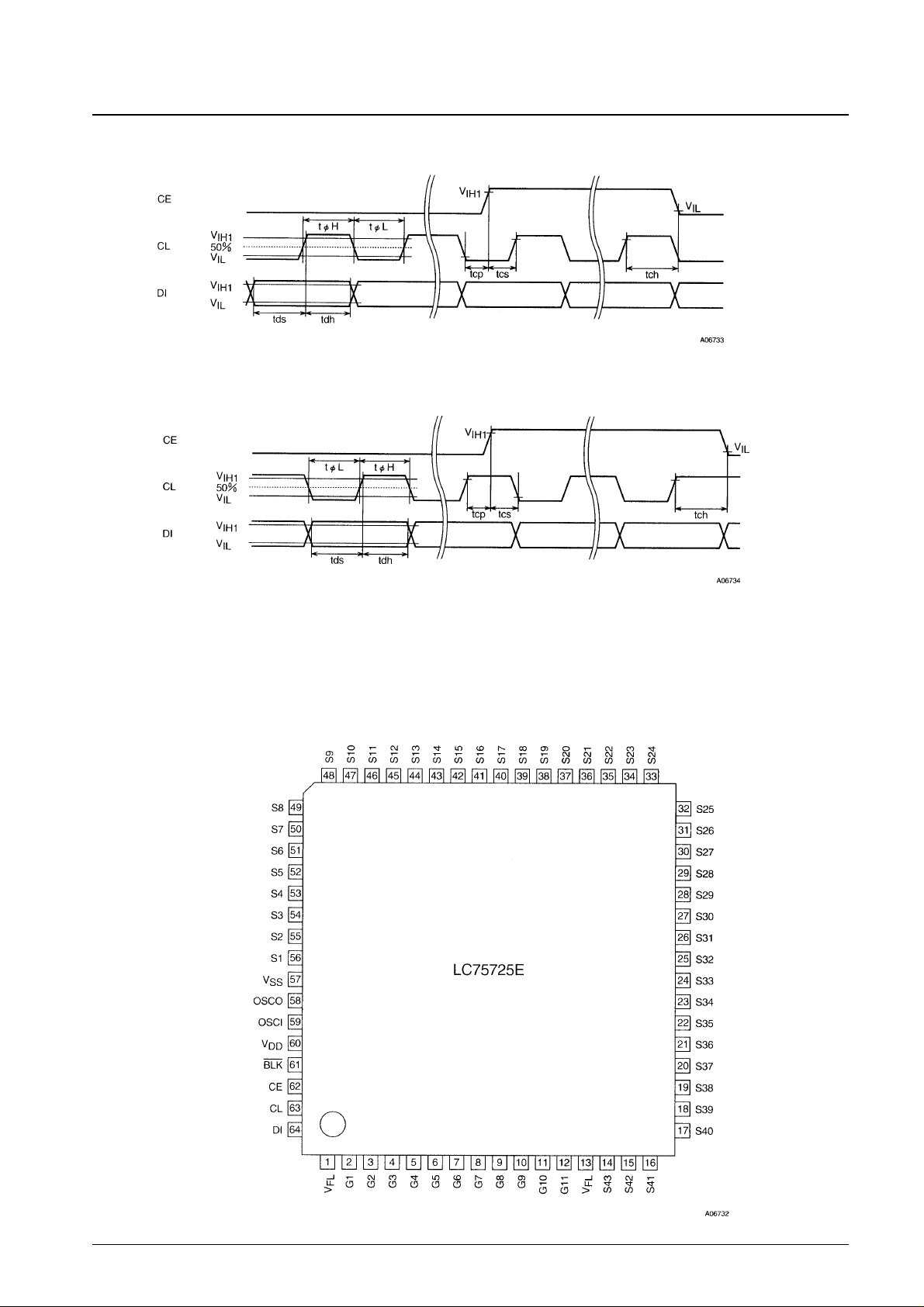
1. When CL is stopped at the low level
2. When CL is stopped at the high level
Pin Assignment
Figure 1
Top view
Page 4
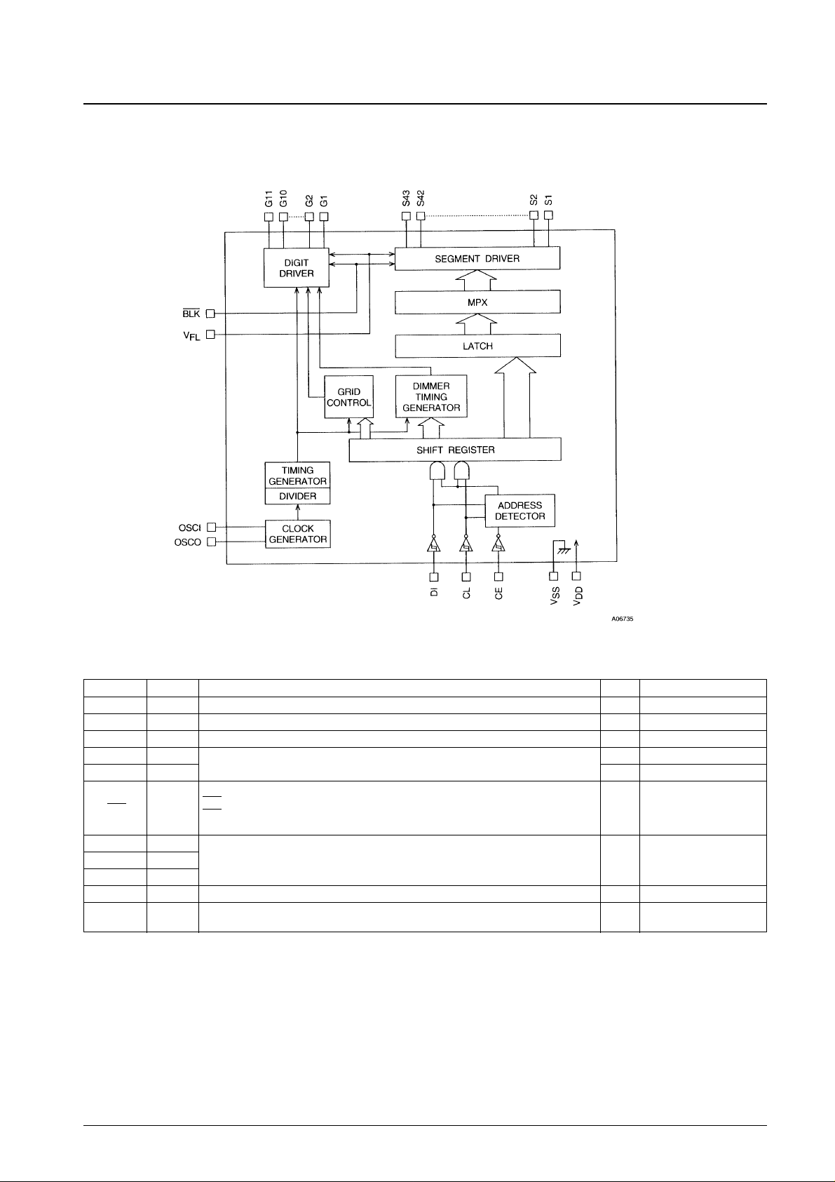
Block Diagram
No. 5606-4/13
LC75725E
Pin Functions
Pin Pin No. Function I/O Handling when unused
V
FL
1, 13 Driver block power supply connection. (Both pins must be connected.) — —
V
DD
60 Logic block power supply connection. Provide a voltage between 4.5 and 5.5 V. — —
V
SS
57 Power supply connection. Connect to the ground. — —
OSCI 59
Oscillator connection. An oscillator circuit is formed by connecting an external resistor
I GND
OSCO 58
and capacitor to these pins.
O OPEN
Display off control input.
BLK 61
BLK = Low (V
SS
) ... Display off. (S1 to S43 and G1 to G11 at VFLlevel.)
I GND
BLK = High (V
DD
) ... Display on.
Note that serial data can be transferred while the display is turned off.
CL 63
DI 64 I GND
CE 62
G1 to G11 2 to 12 Digit outputs. These pins are P-channel open drain outputs with pull-down resistors. O OPEN
S1 to S43 56 to 14
Segment outputs for displaying the display data transferred by serial data input. These pins
O OPEN
are P-channel open drain outputs with pull-down resistors.
Serial data transfer inputs. These pins must be connected to the system microcontroller.
CL: Synchronization clock
DI: Transfer data
CE: Chip enable
Page 5

Serial Data Transfer Format
1. When CL is stopped at the low level
No. 5606-5/13
LC75725E
* : don’t care
DD:direction data
Page 6

No. 5606-6/13
LC75725E
* : don’t care
DD:direction data
Page 7

2. When CL is stopped at the high level
No. 5606-7/13
LC75725E
* : don’t care
DD:direction data
Page 8

Figure 2
No. 5606-8/13
LC75725E
* : don’t care
DD:direction data
Page 9

CCB address: Transfer 01110110B as shown in Figure 2.
DM0 to DM9: Dimmer data
This dimmer data controls the duty of the G1 to G11 digit output pins and the S1 to S43 segment output
pins. It consists of 10 bits, of which DM0 is the LSB. This dimmer data sets the VFD intensity to one of
993 levels. The following table gives the relationship between the dimmer data and the dimmer level.
If distortion of the digit waveforms and segment waveforms by the VFD panel used and the wiring causes
spurious glowing of the VFD panel dimly, we recommend setting the dimmer level to a smaller value.
For example, if the VFD panel displays six digits using digit output pins G1 to G6, set GN0 to 0, GN1 to
1, GN2 to 1, and GN3 to 0.
D1 to D473: Display data
Dn (n=1 to 473) = 1: Display on
Dn (n=1 to 473) = 0: Display off
D1 to D43
. . . . . . . . . .
Display data for digit output G1
D44 to D86
. . . . . . . . .
Display data for digit output G2
D87 to D129
. . . . . . . .
Display data for digit output G3
D130 to D172
. . . . . . .
Display data for digit output G4
D173 to D215
. . . . . . .
Display data for digit output G5
D216 to D258
. . . . . . .
Display data for digit output G6
D259 to D301
. . . . . . .
Display data for digit output G7
D302 to D344
. . . . . . .
Display data for digit output G8
D345 to D387
. . . . . . .
Display data for digit output G9
D388 to D430
. . . . . . .
Display data for digit output G10
D431 to D473
. . . . . . .
Display data for digit output G11
The number of display data bits transferred depends on the number of digits displayed. For example, if the
VFD panel displays six digits, display data bits D1 to D258 are transferred. There is no need to transfer
display data bits D259 to D473.
GN0 to GN3: Number of display digits data
This data give the number of digits displayed by the VFD panel, a number between 4 and 11.
The following table gives the relationship between this setting and the digit output pins used.
No. 5606-9/13
LC75725E
DM9 DM8 DM7 DM6 DM5 DM4 DM3 DM2 DM1 DM0 Dimmer level (Ton/Tdig)
0 0 0 0 0 0 0 0 0 0 0/1024
0 0 0 0 0 0 0 0 0 1 1/1024
0 0 0 0 0 0 0 0 1 0 2/1024
to
1 1 1 1 0 1 1 1 1 0 990/1024
1 1 1 1 0 1 1 1 1 1 991/1024
1 1 1 1 1 0 0 0 0 0 992/1024 (max)
1 1 1 1 1 0 0 0 0 1 992/1024 (max)
to
1 1 1 1 1 1 1 1 0 1 992/1024 (max)
1 1 1 1 1 1 1 1 1 0 992/1024 (max)
1 1 1 1 1 1 1 1 1 1 Not used
Tdig: Single-digit display time (See Figure 4.)
Ton: Single-digit on time (See Figure 4.)
GN3 GN2 GN1 GN0 Digit output pins
0 1 0 0 G1 to G4
0 1 0 1 G1 to G5
0 1 1 0 G1 to G6
0 1 1 1 G1 to G7
1 0 0 0 G1 to G8
1 0 0 1 G1 to G9
1 0 1 0 G1 to G10
1 0 1 1 G1 to G11
to
to
Page 10

Example of Serial Data Transfer
• Six display digits (1/6 duty)
No. 5606-10/13
LC75725E
Page 11

No. 5606-11/13
LC75725E
Correspondence between Display Data (D1 to D473) and Segment Output Pins
Segment output pin G1 G2 G3 G4 G5 G6 G7 G8 G9 G10 G11
S1 D1 D44 D87 D130 D173 D216 D259 D302 D345 D388 D431
S2 D2 D45 D88 D131 D174 D217 D260 D303 D346 D389 D432
S3 D3 D46 D89 D132 D175 D218 D261 D304 D347 D390 D433
S4 D4 D47 D90 D133 D176 D219 D262 D305 D348 D391 D434
S5 D5 D48 D91 D134 D177 D220 D263 D306 D349 D392 D435
S6 D6 D49 D92 D135 D178 D221 D264 D307 D350 D393 D436
S7 D7 D50 D93 D136 D179 D222 D265 D308 D351 D394 D437
S8 D8 D51 D94 D137 D180 D223 D266 D309 D352 D395 D438
S9 D9 D52 D95 D138 D181 D224 D267 D310 D353 D396 D439
S10 D10 D53 D96 D139 D182 D225 D268 D311 D354 D397 D440
S11 D11 D54 D97 D140 D183 D226 D269 D312 D355 D398 D441
S12 D12 D55 D98 D141 D184 D227 D270 D313 D356 D399 D442
S13 D13 D56 D99 D142 D185 D228 D271 D314 D357 D400 D443
S14 D14 D57 D100 D143 D186 D229 D272 D315 D358 D401 D444
S15 D15 D58 D101 D144 D187 D230 D273 D316 D359 D402 D445
S16 D16 D59 D102 D145 D188 D231 D274 D317 D360 D403 D446
S17 D17 D60 D103 D146 D189 D232 D275 D318 D361 D404 D447
S18 D18 D61 D104 D147 D190 D233 D276 D319 D362 D405 D448
S19 D19 D62 D105 D148 D191 D234 D277 D320 D363 D406 D449
S20 D20 D63 D106 D149 D192 D235 D278 D321 D364 D407 D450
S21 D21 D64 D107 D150 D193 D236 D279 D322 D365 D408 D451
S22 D22 D65 D108 D151 D194 D237 D280 D323 D366 D409 D452
S23 D23 D66 D109 D152 D195 D238 D281 D324 D367 D410 D453
S24 D24 D67 D110 D153 D196 D239 D282 D325 D368 D411 D454
S25 D25 D68 D111 D154 D197 D240 D283 D326 D369 D412 D455
S26 D26 D69 D112 D155 D198 D241 D284 D327 D370 D413 D456
S27 D27 D70 D113 D156 D199 D242 D285 D328 D371 D414 D457
S28 D28 D71 D114 D157 D200 D243 D286 D329 D372 D415 D458
S29 D29 D72 D115 D158 D201 D244 D287 D330 D373 D416 D459
S30 D30 D73 D116 D159 D202 D245 D288 D331 D374 D417 D460
S31 D31 D74 D117 D160 D203 D246 D289 D332 D375 D418 D461
S32 D32 D75 D118 D161 D204 D247 D290 D333 D376 D419 D462
S33 D33 D76 D119 D162 D205 D248 D291 D334 D377 D420 D463
S34 D34 D77 D120 D163 D206 D249 D292 D335 D378 D421 D464
S35 D35 D78 D121 D164 D207 D250 D293 D336 D379 D422 D465
S36 D36 D79 D122 D165 D208 D251 D294 D337 D380 D423 D466
S37 D37 D80 D123 D166 D209 D252 D295 D338 D381 D424 D467
S38 D38 D81 D124 D167 D210 D253 D296 D339 D382 D425 D468
S39 D39 D82 D125 D168 D211 D254 D297 D340 D383 D426 D469
S40 D40 D83 D126 D169 D212 D255 D298 D341 D384 D427 D470
S41 D41 D84 D127 D170 D213 D256 D299 D342 D385 D428 D471
S42 D42 D85 D128 D171 D214 D257 D300 D343 D386 D429 D472
S43 D43 D86 D129 D172 D215 D258 D301 D344 D387 D430 D473
Page 12

BLK and the Display Control
Since the LSI internal data (D1 to D473 and the control data) is undefined when power is first applied, the display is off
(S1 to S43 and G1 to G11 pins = VFL level) by setting the BLK pin low at the same time as power is applied.
Then, meaningless display at power on can be prevented by transfering the necessary serial data from the controller while
the display is off and set the BLK pin high after the transfer completes. (See Figure 3.)
Power Supply Sequence
The following sequences must be observed when the power is turned on and off. (See Figure 3.)
• Power on : Logic block power supply (VDD) on →Driver block power supply (VFL) on
• Power off : Driver block power supply (VFL) off →Logic block power supply (VDD) off
Figure 3
No. 5606-12/13
LC75725E
Page 13

Digit Timing Chart (11 display digits)
Tframe, the frame period, is Tdig × N, where N is the number of display digits. Tdig, the single-digit display time, is
2048/fosc, where f
OSC
is the oscillator frequency. When the number of display digits is 11 and the oscillator frequency,
fosc, is 3.7 MHz, Tdig will be about 554 µs and Tframe will be about 6.09 ms.
Figure 4
Sample Application Circuit
PS No. 5606-13/13
LC75725E
This catalog provides information as of March, 1998. Specifications and information herein are subject to
change without notice.
■ No products described or contained herein are intended for use in surgical implants, life-support systems, aerospace
equipment, nuclear power control systems, vehicles, disaster/crime-prevention equipment and the like, the failure of
which may directly or indirectly cause injury, death or property loss.
■ Anyone purchasing any products described or contained herein for an above-mentioned use shall:
➀
Accept full responsibility and indemnify and defend SANYO ELECTRIC CO., LTD., its affiliates, subsidiaries and
distributors and all their officers and employees, jointly and severally, against any and all claims and litigation and all
damages, cost and expenses associated with such use:
➁
Not impose any responsibility for any fault or negligence which may be cited in any such claim or litigation on
SANYO ELECTRIC CO., LTD., its affiliates, subsidiaries and distributors or any of their officers and employees
jointly or severally.
■ Information (including circuit diagrams and circuit parameters) herein is for example only; it is not guaranteed for
volume production. SANYO believes information herein is accurate and reliable, but no guarantees are made or implied
regarding its use or any infringements of intellectual property rights or other rights of third parties.
 Loading...