

Page 1
Ordering number : ENN6866A
90503TN (OT) / 20901RM (OT) No. 6866-1/24
Overview
The LC75421M is an electronic volume controller that
enables control of volume, balance, fader, bass/treble +
super bass, input switching, and input and output level
control functions using only a small number of external
components.
Functions
• Volume:
0 dB to –79 dB in 1-dB steps, and –∞ (81 positions)
Balance function with separate L/R control
• Fader: rear output or front output can be attenuated
across 16 positions (in 2-dB steps from 0 dB to 20 dB, 5-dB steps from –20 dB to –25 dB, 10-dB
steps from –25 dB to –45 dB, and –60 dB, –∞)
• Bass/treble: A tone control circuit can be configured
using an external RC, with 15-position
control from 0 dB to ±11.9 dB in 1.7-dB
steps possible for both bass and treble
• Input gain: 0 dB to +18.75 dB (1.25-dB steps)
amplification is possible for the input signal.
• Output gain: Fader output can be selected among 0 dB,
+6.5 dB, and +8.5 dB.
• Input switching: Five input signals can be selected for
Left and for Right
• Super bass: Step control with 11 positions is possible,
with peaking characteristics (type T)
Features
• On-chip buffer amplifier cuts down number of external
components
• Low switching noise generated by on-chip switch due to
use of silicon gate CMOS process
• On-chip reference voltage circuit for analog ground
• Controls performed with serial input (CCB)
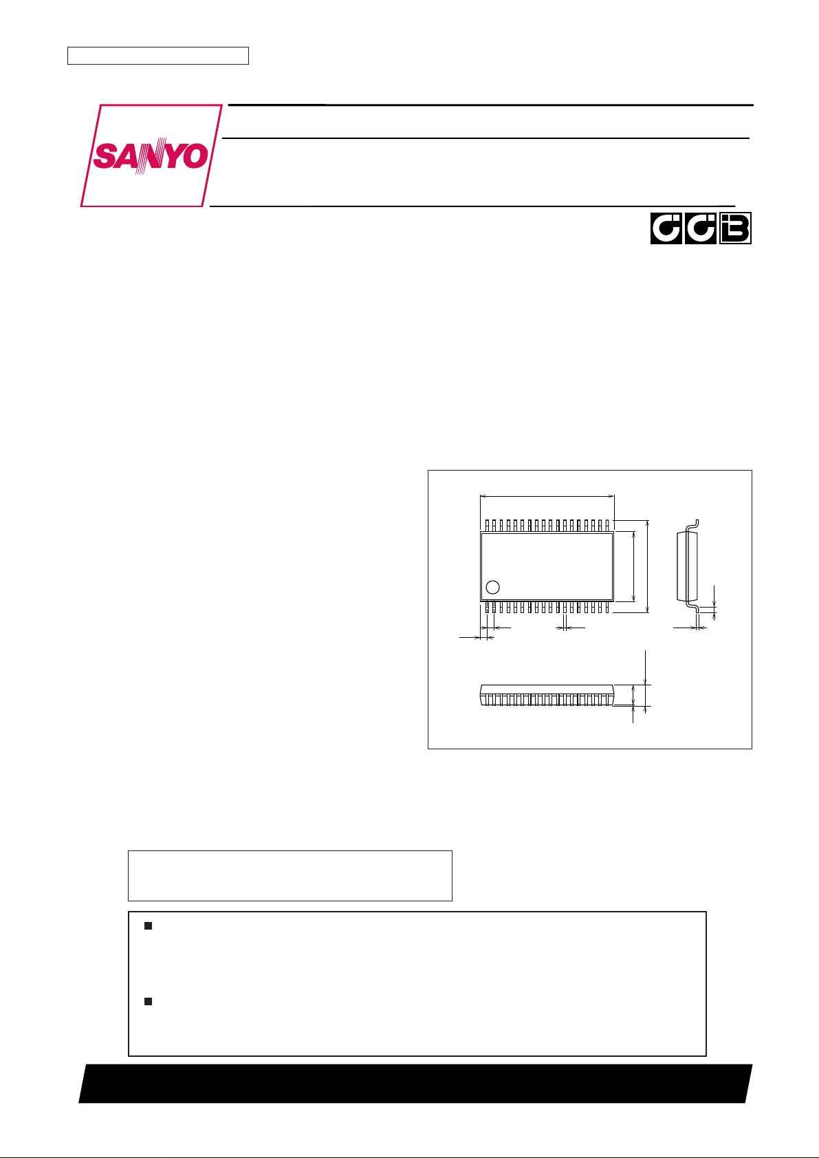
Package Dimensions
unit: mm
3263-MFP36SDJ (375 mil)
1
18
36 19
0.8
15.2
0.3
0.65
10.5
7.9
0.25
(0.8)
2.45max
0.1
(2.25)
SANYO: MFP36SDJ (375 mil)
[LC75421M]
LC75421M
SANYO Electric Co.,Ltd. Semiconductor Company
TOKYO OFFICE Tokyo Bldg., 1-10, 1 Chome, Ueno, Taito-ku, TOKYO, 110-8534 JAPAN
Electronic Volume Controller for Cars
CMOS IC
Any and all SANYO products described or contained herein do not have specifications that can handle
applications that require extremely high levels of reliability, such as life-support systems, aircraft’s
control systems, or other applications whose failure can be reasonably expected to result in serious
physical and/or material damage. Consult with your SANYO representative nearest you before using
any SANYO products described or contained herein in such applications.
SANYO assumes no responsibility for equipment failures that result from using products at values that
exceed, even momentarily, rated values (such as maximum ratings, operating condition ranges, or other
parameters) listed in products specifications of any and all SANYO products described or contained
herein.
• CCB is a trademark of SANYO ELECTRIC CO., LTD.
• CCB is SANYO’s original bus format and all the bus
addresses are controlled by SANYO.
Page 2

Pin Assignment
No. 6866-2/24
LC75421M
LC75421M
1
2
3
4
5
6
7
8
9
10
11
12
13
14
15
16
17
18
36
35
34
33
32
31
30
29
28
27
26
25
24
23
22
21
20
19
DI
CE
VSS
LROUT
LFOUT
LFIN
LOUT
LSB
LBASS2
LBASS1
LTRE
LIN
LSELO
L5
L4
L3
L2
L1
CL
VDD
RROUT
RFOUT
RFIN
ROUT
RSB
RBASS2
RBASS1
RTRE
RIN
RSELO
R5
R4
R3
R2
R1
Vref
Top view
Page 3

No. 6866-3/24
LC75421M
Equivalent Circuit Block Diagram
2.2 µF
2.2 µF
µCOM
2.2 µF
VDD
VSS
CE
DI
CL
2.2 µF
PA
PA
PA
PA
LROUT
4
3 2 1 36 35
RROUT
RFOUT
RFIN
ROUT
1 µF
1 µF
0.15 µF
0.15 µF
3.7 kΩ
RSB
RBASS2
34
33
32
31
30
0.082 µF
0.082 µF
7.68 kΩ
1500 pF
RBASS1
Control
circuit
RVref
LVref
Control
circuit
CCB
interface
Control
circuit
RTRE
RIN
RSELO
29
28
27
25
26
5
6
7
8
9
10
11
12
13
14
1 µF
L5
1 µFL41 µFL31 µFL21 µF
L1
22 µF
Vref
1 µFR11 µF
R2
1 µFR31 µF
R4
1 µF
R5
15 16 17 18 19 20 21 22 23 24
LFOUT
LFIN
LSB
LBASS2
LBASS1
LTRE
LIN
LSELO
0.15 µF
1500 pF
1 µF
0.15 µF
0.082 µF
0.082 µF
1 µF
LOUT
3.7 kΩ
7.68 kΩ
[TREBLE f0 10 kHz] [BASS f0 100 Hz] [S-BASS f0 68 Hz]
Page 4

No. 6866-4/24
LC75421M
Parameter Symbol Conditions Ratings Unit
Maximum supply voltage V
DD
max V
DD
11 V
Maximum input voltage V
IN
max
CE, DI, CL –0.3 to 11
V
Input pins other than CE, DI, CL V
SS
– 0.3 to VDD+ 0.3
Allowable power dissipation Pdmax Ta ≤ 85°C, when mounted on board 550 mW
Operating temperature Topr –40 to +85 °C
Storage temperature Tstg –50 to +125 °C
Specifications
Absolute Maximum Ratings at Ta = 25°C, VSS= 0 V
Parameter Symbol Pin Name Conditions
Ratings
Unit
min typ max
Supply voltage V
DDVDD
7.5 10 V
Input high-level voltage V
IH
CL, DI, CE 4.0 10 V
Input low-level voltage V
IL
CL, DI, CE V
SS
1.0 V
CL, DI, CE, LIN, RIN,
Input amplitude voltage V
IN
L1 to L5, R1 to R5, V
SS
V
DD
Vp-p
LFIN, RFIN
Input pulse width tøW CL 1 µs
Setup time tsetup CL, DI, CE 1 µs
Hold time thold CL, DI, CE 1 µs
Operating frequency fopg CL 500 kHz
Allowable Operating Ranges at Ta = –40 to +85°C, VSS= 0 V
Parameter Symbol Pin Name Conditions
Ratings
Unit
min typ max
Maximum input gain Ginmax +18.75 dB
Step resolution Gstep +1.25 dB
Input resistance Rin
L1, L2, L3, L4, L5
50 kΩ
R1, R2, R3, R4, R5
Clipping level Vcl LSELO, RSELO THD = 1.0%, f = 1 kHz 2.90 Vrms
Output load resistance RL LSELO, RSELO 10 kΩ
Electrical Characteristics at Ta = 25°C, VDD= 8 V, VSS= 0 V
Parameter Symbol Pin Name Conditions
Ratings
Unit
min typ max
Input resistance Rin LIN, RIN 50 kΩ
Volume Block
Parameter Symbol Pin Name Conditions
Ratings
Unit
min typ max
STEP = 0 dB to –20 dB 2
Step resolution ATstep STEP = –20 dB to –25 dB 5 dB
STEP = –25 dB to –45 dB 10
Step error ATerr
STEP = 0 dB to –45 dB –2 0 +2
dB
STEP = –45 dB to –60 dB –3 0 +3
Output load resistance RL 10 kΩ
Output impedance R
O
LFOUT, LROUT RL = 10 kΩ, f = 1 kHz
46 Ω
RFOUT, RROUT V
IN
= 1 Vrms
Fader Volume Block
Page 5

No. 6866-5/24
LC75421M
Parameter Symbol Pin Name Conditions
Ratings
Unit
min typ max
Control range Gbass MAX. Boost/Cut ±10 ±11.9 ±14 dB
Step resolution Estep 1 1.7 3 dB
Internal feedback resistance Rfeed 45.084 kΩ
Bass Band Control Block
Parameter Symbol Pin Name Conditions
Ratings
Unit
min typ max
Control range Gtre MAX. Boost/Cut ±10 ±11.9 ±14 dB
Step resolution Estep 1 1.7 3 dB
Internal feedback resistance Rfeed 56.084 kΩ
Treble Band Control Block
Parameter Symbol Pin Name Conditions
Ratings
Unit
min typ max
Control range Crange MAX. Boost +20 dB
Step resolution Estep +2.0 dB
Internal feedback resistance Rfeed 66.6 kΩ
Super Bass Block (Type T)
Parameter Symbol Conditions
Ratings
Unit
min typ max
Total harmonic distortion THD V
IN
= 1 Vrms, f = 1 kHz, flat overall 0.003 0.01 %
Crosstalk CT V
IN
= 1 Vrms, f = 1 kHz, flat overall, Rg = 1 kΩ 80.5 dB
Maximum attenuated output Vomin V
IN
= 1 Vrms, f = 1 kHz, main volume –∞ –80 dB
Output noise voltage
VN-1 Fflat overall, (IHF-A), RG = 1 kΩ 8 µV
VN-2 Flat overall, (DIN-AUDIO), RG = 1 kΩ 10 µV
Input high-level current I
IH
CL, DI, CE VIN= 8 V 10 µA
Input low-level current I
IL
CL, DI, CE VIN= 0 V –10 µA
General
Page 6

Control Timing and Data Format
To control the LC75421M, input specified serial data to the CE, CL, and DI pins.
The data configuration consists of a total of 52 bits broken down into 8 address bits and 44 data bits.
No. 6866-6/24
LC75421M
CE
B0 B1 B2 B3 A0 A1 A2 A3
1 µs
min
1 µs
min
1 µs
min
1 µs ≤ T
DEST
B
0
D0D1D2D3D4D5D6D7D8D9D10D11D12D13D14D15D16D17D18D19D20D21D22D
23
0
1
0
1
D24D25D26D27D28D29D30D31D32D33D34D35D36D37D38D39D40D41D42D
43
B1B2B3A0A1A2A
3
1 0 0 0 0 0 0 1
1 µs
min
1 µs
min
D0 D1 D2 D3 D4 D5
D38 D39 D40 D41 D42 D43
DI
DI
Super bass control
Treble control
Boost
Boost
Caution: Be sure to set D36 to D38 and D40 to D43
to “0” for the TEST bit of the IC.
CL
CL
CE
Address code
Fader step control
0 0 0 0
1 0 0 0
0 1 0 0
1 1 0 0
0 0 1 0
1 0 1 0
0 1 1 0
1 1 1 0
0 0 0 1
1 0 0 1
0 1 0 1
1 1 0 1
0 0 1 1
1 0 1 1
0 1 1 1
1 1 1 1
–∞ dB
–60 dB
–45 dB
–35 dB
–25 dB
–20 dB
–18 dB
–16 dB
–14 dB
–12 dB
–10 dB
–8 dB
–6 dB
–4 dB
–2 dB
0 dB
0 0 0 0
1 0 0 0
0 1 0 0
1 1 0 0
0 0 1 0
1 0 1 0
0 1 1 0
1 1 1 0
0 0 0 1
1 0 0 1
0 1 0 1
1 1 0 1
0 0 1 1
1 0 1 1
0 1 1 1
1 1 1 1
0 dB
+1.25 dB
+2.50 dB
+3.75 dB
+5.00 dB
+6.25 dB
+7.50 dB
+8.75 dB
+10.00 dB
+11.25 dB
+12.50 dB
+13.75 dB
+15.00 dB
+16.25 dB
+17.50 dB
+18.75 dB
0 0
0 1
1 0
1 1
0 0
1 0
0 1
1 1
0 dB
0 dB
+6.5 dB
+8.5 dB
1 1 1 0
0 1 1 0
1 0 1 0
0 0 1 0
1 1 0 0
0 1 0 0
1 0 0 0
0 0 0 0
1 0 0 1
0 1 0 1
1 1 0 1
0 0 1 1
1 0 1 1
0 1 1 1
1 1 1 1
STEP15
STEP14
STEP13
STEP12
STEP11
STEP10
STEP9
STEP8
STEP7
STEP6
STEP5
STEP4
STEP3
STEP2
STEP1
Cut
1 1 1 0
0 1 1 0
1 0 1 0
0 0 1 0
1 1 0 0
0 1 0 0
1 0 0 0
0 0 0 0
1 0 0 1
0 1 0 1
1 1 0 1
0 0 1 1
1 0 1 1
0 1 1 1
1 1 1 1
STEP15
STEP14
STEP13
STEP12
STEP11
STEP10
STEP9
STEP8
STEP7
STEP6
STEP5
STEP4
STEP3
STEP2
STEP1
Cut
0 0 0 0
1 0 0 0
0 1 0 0
1 1 0 0
0 0 1 0
1 0 1 0
0 1 1 0
1 1 1 0
0 0 0 1
1 0 0 1
0 1 0 1
STEP0(FLAT)
STEP1
STEP2
STEP3
STEP4
STEP5
STEP6
STEP7
STEP8
STEP9
STEP10
(BOOST max)
Bass control
Volume control
Fader
rear/front
control
Rear
Front
OFF
ON
TEST mode
Input switch control (1) Input switch control (2)
Input mute
switch control
Input gain control
Channel selection
Initial setting
Lch
Rch
L/R simultaneous
Output gain control
Page 7

No. 6866-7/24
LC75421M
Volume Control
D16 D17 D18 D19 D20 D21 D22 D23 Operation
0 0 1 0 0 1 0 1 0dB
1 1 0 0 0 1 0 1 –1dB
0 1 0 0 0 1 0 1 –2dB
1 0 0 0 0 1 0 1 –3dB
0 0 1 1 1 0 0 1 –4dB
1 1 0 1 1 0 0 1 –5dB
0 1 0 1 1 0 0 1 –6dB
1 0 0 1 1 0 0 1 –7dB
0 0 1 0 1 0 0 1 –8dB
1 1 0 0 1 0 0 1 –9dB
0 1 0 0 1 0 0 1 –10dB
1 0 0 0 1 0 0 1 –11dB
0 0 1 1 0 0 0 1 –12dB
1 1 0 1 0 0 0 1 –13dB
0 1 0 1 0 0 0 1 –14dB
1 0 0 1 0 0 0 1 –15dB
0 0 1 0 0 0 0 1 –16dB
1 1 0 0 0 0 0 1 –17dB
0 1 0 0 0 0 0 1 –18dB
1 0 0 0 0 0 0 1 –19dB
0 0 1 1 1 1 1 0 –20dB
1 1 0 1 1 1 1 0 –21dB
0 1 0 1 1 1 1 0 –22dB
1 0 0 1 1 1 1 0 –23dB
0 0 1 0 1 1 1 0 –24dB
1 1 0 0 1 1 1 0 –25dB
0 1 0 0 1 1 1 0 –26dB
1 0 0 0 1 1 1 0 –27dB
0 0 1 1 0 1 1 0 –28dB
1 1 0 1 0 1 1 0 –29dB
0 1 0 1 0 1 1 0 –30dB
1 0 0 1 0 1 1 0 –31dB
0 0 1 0 0 1 1 0 –32dB
1 1 0 0 0 1 1 0 –33dB
0 1 0 0 0 1 1 0 –34dB
1 0 0 0 0 1 1 0 –35dB
0 0 1 1 1 0 1 0 –36dB
1 1 0 1 1 0 1 0 –37dB
0 1 0 1 1 0 1 0 –38dB
1 0 0 1 1 0 1 0 –39dB
0 0 1 0 1 0 1 0 –40dB
1 1 0 0 1 0 1 0 –41dB
0 1 0 0 1 0 1 0 –42dB
1 0 0 0 1 0 1 0 –43dB
0 0 1 1 0 0 1 0 –44dB
1 1 0 1 0 0 1 0 –45dB
0 1 0 1 0 0 1 0 –46dB
1 0 0 1 0 0 1 0 –47dB
0 0 1 0 0 0 1 0 –48dB
1 1 0 0 0 0 1 0 –49dB
0 1 0 0 0 0 1 0 –50dB
Continued on next page.
Page 8

No. 6866-8/24
LC75421M
Continued from preceding page.
D16 D17 D18 D19 D20 D21 D22 D23 Operation
1 0 0 0 0 0 1 0 –51dB
0 0 1 1 1 1 0 0 –52dB
1 1 0 1 1 1 0 0 –53dB
0 1 0 1 1 1 0 0 –54dB
1 0 0 1 1 1 0 0 –55dB
0 0 1 0 1 1 0 0 –56dB
1 1 0 0 1 1 0 0 –57dB
0 1 0 0 1 1 0 0 –58dB
1 0 0 0 1 1 0 0 –59dB
0 0 1 1 0 1 0 0 –60dB
1 1 0 1 0 1 0 0 –61dB
0 1 0 1 0 1 0 0 –62dB
1 0 0 1 0 1 0 0 –63dB
0 0 1 0 0 1 0 0 –64dB
1 1 0 0 0 1 0 0 –65dB
0 1 0 0 0 1 0 0 –66dB
1 0 0 0 0 1 0 0 –67dB
0 0 1 1 1 0 0 0 –68dB
1 1 0 1 1 0 0 0 –69dB
0 1 0 1 1 0 0 0 –70dB
1 0 0 1 1 0 0 0 –71dB
0 0 1 0 1 0 0 0 –72dB
1 1 0 0 1 0 0 0 –73dB
0 1 0 0 1 0 0 0 –74dB
1 0 0 0 1 0 0 0 –75dB
0 0 1 1 0 0 0 0 –76dB
1 1 0 1 0 0 0 0 –77dB
0 1 0 1 0 0 0 0 –78dB
1 0 0 1 0 0 0 0 –79dB
0 0 0 0 0 0 0 0 –∞dB
Input Switch Control (L1, L2, L3, L4, L5, R1, R2, R3, R4, R5)
D28 D29 D32 Operation
0 0 1 L1 (R1) ON
1 0 1 L2 (R2) ON
0 1 1 L3 (R3) ON
1 1 1 L4 (R4) ON
0 0 0 L5 (R5) ON
Page 9

No. 6866-9/24
LC75421M
Pin Functions
Pin No. Pin Name Function Equivalent circuit
• Input signal pins
18
17
16
15
14
20
21
22
23
24
L1
L2
L3
L4
L5
R1
R2
R3
R4
R5
VDD
VDD
SELO
Ln
Rn
Vref
VDD
VDDVDD
BASS1 BASS2
• Input selector output pins
13
25
LSELO
RSELO
• Bass band filter configuration capacitor and resistor
connection pins
10
9
28
29
LBASS1
LBASS2
RBASS1
RBASS2
VDD
VDDVDD
SB OUT
• Super bass band filter configuration capacitor and resistor
connection pins
8
7
30
31
LSB
LOUT
RSB
ROUT
VDD
• Fader output pins. The front side and rear side can be
attenuated separately. The attenuation is the same for both
Left and Right.
5
4
33
34
LFOUT
LROUT
RFOUT
RROUT
Continued on next page.
Page 10

No. 6866-10/24
LC75421M
Continued from preceding page.
Pin No. Pin Name Function Equivalent circuit
• Capacitor connection pin for configuring treble filter
11
27
LTRE
RTRE
VDD
TRE
• Connect a capacitor of a few tens of µF between Vref and
AV
SS(VSS
) as a analog ground 0.5 × VDDvoltage
generator, current ripple countermeasure.
19 Vref
VDD
Vref
VDD
• Ground pin 3
V
SS
• Power supply pin35
V
DD
• Chip enable pin
Data is written to the internal latch and the analog switches
are operated when the level changes from High to Low.
Data transfer is enabled when the level is High.
2 CE
• Serial data pin and clock input pin for control
1
36
DI
CL
Page 11

No. 6866-11/24
LC75421M
Equivalent Circuit Input Block Diagram
L1
LSEL0
TOTAL = 50 k
LVref
Same for right channel
Unit: (Resistance: Ω)
6.702 k
0 dB
5.804 k
+1.25 dB
5.026 k
+2.50 dB
4.352 k
+3.75 dB
3.769 k
+5.00 dB
3.264 k
+6.25 dB
2.826 k
+7.50 dB
2.447 k
+8.75 dB
2.119 k
+10.00 dB
1.835 k
+11.25 dB
1.589 k
+12.50 dB
1.376 k
+13.75 dB
1.192 k
+15.00 dB
1.032 k
+16.25 dB
0.894 k
+17.50 dB
5.774 k
+18.75 dB
L2
L3
L4
L5
50 k
50 k
50 k
50 k
50 k
Page 12

No. 6866-12/24
LC75421M
Volume Block Equivalent Circuit Diagram
LIN
R1 = 5434
0 dB
R2 = 4845
–1 dB
R3 = 4319
–2 dB
R4 = 3850
–3 dB
R5 = 3431
–4 dB
R6 = 3058
–5 dB
R7 = 2726
–6 dB
R8 = 2429
–7 dB
R9 = 2165
–8 dB
R10 = 1930
–9 dB
R11 = 1720
–10 dB
R12 = 1533
–11 dB
R13 = 1366
–12 dB
R14 = 1218
–13 dB
R15 = 1085
–14 dB
R16 = 967
–15 dB
R17 = 862
–16 dB
R18 = 768
–17 dB
R19 = 685
–18 dB
R20 = 610
–19 dB
R21 = 544
–20 dB
R22 = 485
–21 dB
R23 = 432
–22 dB
R24 = 385
–23 dB
R25 = 343
–24 dB
R26 = 306
–25 dB
R27 = 273
–26 dB
R28 = 243
R29 = 216
–28 dB
R30 = 193
–29 dB
R31 = 172
–30 dB
R32 = 153
–31 dB
R33 = 137
–32 dB
R34 = 122
–33 dB
R35 = 108
–34 dB
R36 = 97
–35 dB
R37 = 86
–36 dB
R38 = 77
–37 dB
R39 = 68
–38 dB
R40 = 61
–39 dB
R41 = 54
–40 dB
R42 = 48
–41 dB
R43 = 86
–42 dB
R44 = 77
–43 dB
R45 = 69
–44 dB
R46 = 61
–45 dB
R47 = 55
–46 dB
R48 = 49
–47 dB
R49 = 87
–48 dB
R50 = 77
–49 dB
R51 = 69
–50 dB
R52 = 61
–51 dB
R53 = 55
–52 dB
R54 = 49
–53 dB
–54 dB
794
R81
796
R82
798
R83
800
R84
802
R85
804
R86
Same for right channel
Unit: (Resistance: Ω)
LVref
R55 = 87
R56 = 77
–55 dB
To
Treble
Block
R57 = 69
–56 dB
R58 = 61
–57 dB
R59 = 55
–58 dB
R60 = 49
–59 dB
R61 = 87
–60 dB
R62 = 78
–61 dB
R63 = 69
–62 dB
R64 = 62
–63 dB
R65 = 55
–64 dB
R66 = 49
–65 dB
R67 = 87
–66 dB
R68 = 78
–67 dB
R69 = 69
–68 dB
R70 = 62
–69 dB
R71 = 55
–70 dB
R72 = 49
–71 dB
R73 = 87
–72 dB
R74 = 78
–73 dB
R75 = 69
–74 dB
R76 = 62
–75 dB
R77 = 55
–76 dB
R78 = 49
–77 dB
R79 = 44
–78 dB
R80 = 359
–79 dB
–∞ dB
–27 dB
Page 13

No. 6866-13/24
LC75421M
Treble/Bass/Super Bass Band Block Equivalent Circuit Diagram
From
Volume
Block
Same for right channel
Unit: (Resistance: Ω)
SW1
LTRE
Total = 56.084 k
±11.9 dB11.030 k
±10.2 dB
±8.5 dB
±6.8 dB
±5.1 dB
±3.4 dB
±1.7 dB
0 dB
2.908 k
3.661 k
4.608 k
5.802 k
7.304 k
9.195 k
11.576 k
LSB
During boost, SW1 and SW3 are ON, during cut, SW2 and SW4 are ON,
when 0 dB, 0 dB SW and SW2 and SW3 are ON.
Total = 66.6 k
+18 dB
+4 dB
+2 dB
0 dB
+20 dB
+16 dB
+14 dB
+12 dB
+10 dB
+8 dB
±6 dB
1.916 k
2.412 k
3.037 k
3.823 k
4.813 k
6.059 k
7.628 k
9.603 k
12.089 k
15.220 k
SW2
SW3
SW4
SW1
LBASS1
LOUT
LBASS2Total = 45.084 k
±11.9 dB0.030 k
±10.2 dB
±8.5 dB
±6.8 dB
±5.1 dB
±3.4 dB
±1.7 dB
0 dB
2.908 k
3.661 k
4.608 k
5.802 k
7.304 k
9.195 k
11.576 k
SW2
SW3
SW4
Same for right channel
Units: (Resistance: Ω)
Page 14

No. 6866-14/24
LC75421M
Fader Volume Block Equivalent Circuit Diagram
LFIN
S1
S2
0 dB
26.342 k
4.866 k
50 k
18.792 k
+6.5 dB
+8.5 dB
0 dB
26.342 k
4.866 k
50 k
18.792 k
Same for right channel
Unit: (Resistance: Ω)
When FADER = “1”, S2 and S3 are ON
When FADER = “0”, S1 and S4 are ON
Total = 50 k
+6.5 dB
+8.5 dB
S4
S3
LFOUT LROUT
LVref
When –∞ data is sent to the main volume, S1 and S2 become open, and S3 and S4 simultaneously become ON.
10.284 k
8.169 k
6.489 k
5.154 k
4.094 k
3.252 k
2.583 k
2.052 k
1.630 k
1.295 k
2.188 k
1.923 k
0.608 k
0.231 k
0.050 k
0 dB
–2 dB
–4 dB
–6 dB
–8 dB
–10 dB
–12 dB
–14 dB
–16 dB
–18 dB
–20 dB
–25 dB
–35 dB
–45 dB
–60 dB
–∞ dB
Page 15

Tone Circuit Constant Calculation Examples
Super Bass Band Circuit
The equivalent circuit and the formula for calculating the external RC with a mean frequency of 68 Hz are shown
below.
• Super bass band equivalent circuit block diagram
• Calculation example
Specification Mean frequency: f0 = 68 Hz
Gain during maximum boost: G = 20 dB
Let us use R1 = 0, R2 = 66.6 kΩ, and C1 = C2 = C.
We obtain R3 from G = 20 dB.
We obtain C from mean frequency f0 = 68 Hz.
We obtain Q.
No. 6866-15/24
LC75421M
C1
R1 R2
R3
C2
G
+20 dB
= 20 × LOG10 1 +
R2
2R3
R3 =
R2
2 10
G+20dB/20
–1
66600
2
× (10 – 1)
= ≠ 3.7 KΩ
f 0 =
R3R2C1C2
1
2π
C = =
1
2
πf0 R3R2
1
2π × 68 66600 × 3700
≠ 0.15 µF
Q =
R3R2
R3R2
2R3
1
≠ 2.1
Page 16

Treble Band Circuit
The shelving characteristics can be obtained for the treble band.
The equivalent circuit and calculation formula during boost are indicated below.
• Calculation example 1
Specification Set frequency: f = 10000 Hz
Gain during maximum boost: G
+ 14 dB
= 14 dB
Let us use R1 = 11.030 kΩ and R2 = 45.054 kΩ.
The above constants are inserted in the following formula.
No. 6866-16/24
LC75421M
C
R1 R2
C =
R2
)
2
– R1
2
1
2
πf
10
G/20
– 1
(
=
1
2
π10000
45054
5.01–1
≠ 6800(pF)
( )
2
– 11030
2
R2
R1
2
+ (1 / ωC)
2
G = 20 × LOG10 1 +
Simulation Results
Setting f = 10 kHz f = 1 kHz
14 dB 13.95 7.42
12 dB 11.98 6.96
10 dB 10 6.34
8 dB 8 5.5
6 dB 6 4.43
4 dB 4 3.13
2 dB 2 1.64
Page 17

No. 6866-17/24
LC75421M
• Calculation example 2
Specification Set frequency: f = 10000 Hz
Gain during maximum boost: G
+ 11.9 dB
= 11.9 dB
Let us use R1 = 11.030 kΩ and R2 = 45.054 kΩ.
The above constants are inserted in the following formula.
R2
R1
2
+ (1 / ωC)
2
C =
R2
)
2
– R1
2
1
2
πf
10
11.9/20
– 1
(
=
1
2
π10000
45054
3.94–1
≠ 1500(pF)
( )
2
– 11030
2
G = 20 × LOG10 1 +
Setting f = 10 kHz f = 1 kHz
11.9 dB 11.92 0.00
10.2 dB 10.64 0.00
8.5 dB 9.17 0.00
6.8 dB 7.52 0.00
5.1 dB 5.74 0.00
3.4 dB 3.88 0.00
1.7 dB 1.96 0.00
Simulation Results
Page 18

No. 6866-18/24
LC75421M
Bass Shelving Circuit
The equivalent circuit and calculation formula during boost are shown below.
• Bass band equivalent circuit diagram
• Calculation example 1
Specification Mean frequency: f0 = 40 Hz
Gain during maximum boost: G
+ 14 dB
= 14 dB
Let us use R1 = 0 kΩ, R2 = 45.054 kΩ, C1 = 2.2 µF, and C1 >> C2.
We obtain R3 from G = 14 dB.
We obtain C2 from mean frequency f0 = 40 Hz.
R1 R2
R3
C1 C2
G
+14 dB
= 20 × LOG
10
R2 + R3
R3
R3 =
R2
10
G/20
–1
45054
5.01 – 1
= ≠ 11 KΩ
f 0 =
R3R2C1C2
1
2π
C2 = =
1
(2
πf0)
2
R2R3C1
1
(2
π × 40)
2
× 45054 × 11000 × (2.2 × 10–6)
≠ 0.015 µF
Simulation Results
Setting f = 100 Hz f = 1 kHz
14 dB 13.55 3.65
12 dB 11.73 3.51
10 dB 9.8 3.31
8 dB 7.89 3
6 dB 5.94 2.55
4 dB 3.97 1.92
2 dB 1.99 1.07
Page 19

No. 6866-19/24
LC75421M
• Calculation example 2
Specification Mean frequency: f0 = 40 Hz
Gain during maximum boost: G = 12 dB
Let us use R1 = 0 kΩ, R2 = 45.054 kΩ, C1 = 2.2 uF, and C1 >> C2.
We obtain R3 from G = 12 dB.
We obtain C2 from mean frequency f0 = 40 Hz.
G
+12 dB
= 20 × LOG
10
R2 + R3
R3
R3 =
R2
10
G/20
–1
45054
3.98 – 1
= ≠ 15 KΩ
f 0 =
R3R2C1C2
1
2π
C2 = =
1
(2
πf0)
2
R2R3C1
1
(2
π × 40)
2
× 45054 × 15000 × (2.2 × 10–6)
≠ 0.01 µF
Setting f = 100 Hz f = 1 kHz
14 dB 11.73 4.27
12 dB 10.29 4.07
10 dB 8.74 3.78
8 dB 7.11 3.38
6 dB 5.41 2.82
4 dB 3.65 2.09
2 dB 1.85 1.15
Simulation Results
Page 20

No. 6866-20/24
LC75421M
(4) Bass Peaking Circuit
The equivalent circuit and the formula for calculating the external RC with a mean frequency of 100 Hz are shown
below.
• Bass band equivalent circuit diagram
• Calculation example
Specification Mean frequency: f0 = 100 Hz
Gain during maximum boost: G = 11.9 dB
Let us use R1 = 0, R2 = 45.084 kΩ, and C1 = C2 = C.
We obtain R3 from G = 11.9 dB.
We obtain C from mean frequency f0 = 100 Hz.
We obtain Q.
C1 C2
R1 R2
R3
G
+11.9 dB
= 20 × LOG10 1 +
R2
2R3
R3 =
R2
2 10
11.9dB/20
–1
45084
2
× (3.936 – 1)
= ≠ 7.68 KΩ
f 0 =
R3R2C1C2
1
2π
C = =
1
2
πf0 R3R2
1
2π × 100 45084 × 7680
≠ 0.082 µF
Q =
R3R2
R3R2
2R3
1
•
≠ 1.66
Simulation Results
Setting f = 100 Hz f = 1 kHz
11.9 dB 11.88 0.00
10.2 dB 10.38 0.00
8.5 dB 8.79 0.00
6.8 dB 7.14 0.00
5.1 dB 5.42 0.00
3.4 dB 3.66 0.00
1.7 dB 1.85 0.00
Page 21

No. 6866-21/24
LC75421M
Usage Cautions
(1) Upon power application, the internal analog switch status is undefined. Use an external countermeasure such as
muting until data is set.
(2) When performing initial data setting after applying power, send the initial data once, and then send the initial setting
data.
(3) To ensure that the digital frequency signal sent to the CL, DI, and CE pins do not spill over to the analog signal
block, either guard these signal lines with a ground pattern, or perform transmission using shielded wires.
Page 22

No. 6866-22/24
LC75421M
Main volume control block
Input gain block
Fader block
Graphic equalizer block
Main volume control block
Main volume control block
Input gain block
Input gain block
Fader block
Fader block
THD
METER
Graphic equalizer block
Graphic equalizer block
Main volume control block
Input gain block
Fader block
Graphic equalizer block
Main Volume Control Step Characteristics Input Gain Step Characteristics
THD — Frequency CharacteristicsFader Step Characteristics
Attenuation — dB
Step setting — dB
Output level — dB
Step setting — dB
Attenuation — dB
Step setting — dB
Total harmonic distortion, THD — %
Frequency, f — Hz
Page 23

No. 6866-23/24
LC75421M
Main volume control block
Input gain block
Fader block
THD
METER
Graphic equalizer block
Main volume control block
Input gain block
Fader block
THD
METER
Graphic equalizer block
THD — Input Level Characteristics
Total harmonic distortion, THD — %
Input level, VIN — dBV
Bass Control Characteristics Treble Control Characteristics
Super Bass Characteristics
Level — dBLevel — dB
Frequency, f — Hz
Level — dB
Frequency, f — Hz
Frequency, f — Hz
THD — Supply Voltage Characteristics
Total harmonic distortion, THD — %
Supply voltage — V
Page 24

PS No. 6866-24/24
LC75421M
This catalog provides information as of September, 2003. Specifications and information herein are
subject to change without notice.
Specifications of any and all SANYO products described or contained herein stipulate the performance,
characteristics, and functions of the described products in the independent state, and are not guarantees
of the performance, characteristics, and functions of the described products as mounted in the customer’s
products or equipment. To verify symptoms and states that cannot be evaluated in an independent device,
the customer should always evaluate and test devices mounted in the customer’s products or equipment.
SANYO Electric Co., Ltd. strives to supply high-quality high-reliability products. However, any and all
semiconductor products fail with some probability. It is possible that these probabilistic failures could
give rise to accidents or events that could endanger human lives, that could give rise to smoke or fire,
or that could cause damage to other property. When designing equipment, adopt safety measures so
that these kinds of accidents or events cannot occur. Such measures include but are not limited to protective
circuits and error prevention circuits for safe design, redundant design, and structural design.
In the event that any or all SANYO products (including technical data, services) described or contained
herein are controlled under any of applicable local export control laws and regulations, such products must
not be exported without obtaining the export license from the authorities concerned in accordance with the
above law.
No part of this publication may be reproduced or transmitted in any form or by any means, electronic or
mechanical, including photocopying and recording, or any information storage or retrieval system,
or otherwise, without the prior written permission of SANYO Electric Co., Ltd.
Any and all information described or contained herein are subject to change without notice due to
product/technology improvement, etc. When designing equipment, refer to the “Delivery Specification”
for the SANYO product that you intend to use.
Information (including circuit diagrams and circuit parameters) herein is for example only; it is not
guaranteed for volume production. SANYO believes information herein is accurate and reliable, but
no guarantees are made or implied regarding its use or any infringements of intellectual property rights
or other rights of third parties.
 Loading...