

Page 1
Ordering number : ENN7053
O1901RM (OT) No. 7053-1/21
Overview
The LC75412E and 75412W are electronic volume
controllers that enable control of volume, balance, fader,
bass/treble, loudness, input switching, and input gain
using only a small number of external components.
Functions
• Volume: 0 d B to –79 dB in 1-dB steps, and –∞ (81
positions) Balance function with separate L/R
control
• Fader: rear output or front output can be attenuated
across 16 positions (in 1-dB steps from 0 dB to
–2 dB, 2-dB steps from –2 dB to –20 dB, 10-dB
steps from –20 dB to –30 dB, and –45 dB,
–60 dB, –∞)
• Bass/treble: Each band can be controlled in 2-dB steps
from ±0 dB to ±18 dB.
• Input gain: 0 dB to +18.75 dB (1.25-dB steps)
amplification is possible for the input signal.
• Input switching: Six input signals can be selected for
Left and for Right (five are singleended inputs and one is a differential
input.)
• Loudness: A tap is output from the –32 dB position of a
volume control resistor ladder. A loudness
function can be implemented by connecting
an external RC circuit.
Features
• On-chip buffer amplifier cuts down number of external
components
• Low switching noise generated by on-chip switch
through use of silicon gate CMOS process, for low
switching noise when there is no signal
• Low switching noise when there is a signal due to use
of on-chip zero-cross switching circuit
• On-chip 1/2 VDD reference voltage circuit
• Controls performed with serial input (CCB)
LC75412E, 75412W
SANYO Electric Co.,Ltd. Semiconductor Company
TOKYO OFFICE Tokyo Bldg., 1-10, 1 Chome, Ueno, Taito-ku, TOKYO, 110-8534 JAPAN
Electronic Volume Controller
for Car Audio Systems
CMOS IC
Any and all SANYO products described or contained herein do not have specifications that can handle
applications that require extremely high levels of reliability, such as life-support systems, aircraft’s
control systems, or other applications whose failure can be reasonably expected to result in serious
physical and/or material damage. Consult with your SANYO representative nearest you before using
any SANYO products described or contained herein in such applications.
SANYO assumes no responsibility for equipment failures that result from using products at values that
exceed, even momentarily, rated values (such as maximum ratings, operating condition ranges, or other
parameters) listed in products specifications of any and all SANYO products described or contained
herein.
• CCB is a trademark of SANYO ELECTRIC CO., LTD.
• CCB is SANYO’s original bus format and all the bus
addresses are controlled by SANYO.
Page 2
No. 7053-2/21
LC75412E, 75412W
Package Dimensions
unit: mm
3159-QIP64E
unit: mm
3190-SQFP64
14.0
17.2
1.0
1.0
1.6
0.15
0.35
0.1
15.6
0.8
0.8
3.0max
1
16
17
32
33
48
49
64
2.7
14.0
17.2
1.0
1.0
1.6
0.8
SANYO: QIP64E
[LC75412E]
10.0
12.0
1.25
0.5
1.25
1.25 0.5 1.250.18
12.0
1 16
17
32
33
48
49
64
10.0
0.5
1.7max
0.5
0.1
0.15
SANYO: SQFP64
[LC75412W]
Pin Assignment
LC75412E/W
5 4 3 2 1 11 10 9 8 7 6
RSELO
RVRIN
RCT
NCNCNC
RF1C1
RF1C2
RF1C3
NC
NC
21
20
19
18
17
27
26
25
24
23
22
RFIN
RFOUT
RROUT
TIM
NC
RAVSS
MUTE
CE
DI
CL
DVSS
12
28
NC
13
RF3C114RF3C215RF3C3
16
4445464748 383940414243 37 36 35 34 33
RTOUT
TEST
29
LAVSS
30
LROUT
31
LFOUT
32
60
61
62
63
64
54
55
56
57
58
59
53
52
51
50
49
LFIN
R5P
R5M
R4
R3
R2
R1
R6
Vref
VDD
L6
L1
L2
L3
L4
L5M
L5P
LSELO
LVRIN
LCTNCNCNCLF1C1
LF1C2
LF1C3NCNCNCLF3C1
LF3C2
LF3C3
LTOUT
Page 3
No. 7053-3/21
LC75412E, 75412W
Equivalent Circuit Block Diagram/Sample Application Circuit
0.033µF
L5P
+
LFIN
RFIN
NC
TIM
RAVSS
CE
DI
CL
ZEROCROSS DET
MUTE
TEST
DVSS
VDD
L6
1µF × 7
1µF × 7
10µF
1µF
1000pF
0.001µF
0.001µF
0.1µF
0.1µF
LTOUT
LF3C2
LF3C3
LF3C1
NC
NC
NC
NC
NC
NC
LF1C2
LF1C3
LF1C1
10kΩ
1kΩ
0.33µF
LCT
LVRIN
LSELO
NO SIGNAL
TIMER
Multiplexer
0.001µF
10µF
RTOUT
RF3C2
RF3C3
RF3C1
NC
NC
NC
0.1µF
0.001µF
0.1µF
RF1C2
RF1C3
RF1C1
LVref
LVref
LVref
RVref
LVref
+
Vref
22µF
+
+
R6
+
RVref LVref
RVref
RVref
1MΩ
47kΩ
NC
NC
NC
RSELO
RVRIN
RCT
1000pF
1µF
10kΩ
1kΩ
0.33µF
RVref
49
50
53
54
55
56
57
58
59
60
63
64
L5M
+
10µF
LROUT
LFOUT
10µF
PA
PA
10µF
RFOUT
RROUT
10µF
L4+L3+L2+L1
+
R1+R2+R3+R4
+
R5M
+
R5P
+
+
+
32
31
29
28
27
26
25
24
23
22
21
20
17
CCB
INTERFACE
DI
CE
CL
µCOM
LAVSS
1 2 3 4 5 6 10 11 12 14 15 16
30
48 47 45 44 43 42 41 40 39 38 37 36 35 34 3346
Multiplexer
19
18
PA
PA
ZEROCROSS DET
LOGIC CIRCUIT
CONTROL
CIRCUIT
7 8 9
61
62
51
52
13
Page 4
No. 7053-4/21
LC75412E, 75412W
Parameter Symbol Conditions Ratings Unit
Maximum supply voltage V
DD
max V
DD
11 V
Maximum input voltage V
IN
max All input pins VSS– 0.3 to VDD+ 0.3 V
Allowable power dissipation Pd max Ta ≤ 85°C, when mounted on board
QIP64E 680
mW
SQFP64 800
Operating temperature Topr –40 to +85 °C
Storage temperature Tstg –50 to +125 °C
Specifications
Absolute Maximum Ratings at Ta = 25°C, VSS= 0 V
Parameter Symbol Conditions
Ratings
Unit
min typ max
Supply voltage V
DDVDD
6.0 10 V
Input high-level voltage V
IH
CL, DI, CE 4.0 10 V
Input low-level voltage V
IL
CL, DI, CE V
SS
1.0 V
Input amplitude voltage V
IN
V
SS
V
DD
Vp-p
Input pulse width TøW CL 1 µs
Setup time Tsetup CL, DI, CE 1 µs
Hold time Thold CL, DI, CE 1 µs
Operating frequency fopg CL 500 kHz
Allowable Operating Ranges at Ta = 25°C, VSS= 0 V
Parameter Symbol Pin Name Conditions
Ratings
Unit
min typ max
[Input block]
Input resistance Rin L1 to L4, L6, R1 to R4, R6 25 50 100 kΩ
Minimum input gain Ginmin L1 to L4, L6, R1 to R4, R6 –1 0 +1 dB
Maximum input gain Ginmax +16.5 +18.75 +21 dB
Step setting error ATerr ±0.5 dB
L/R balance BAL ±0.5 dB
[Volume Block]
Input resistance Rvr LVRIN, RVRIN, loudness off 25 50 100 kΩ
Step setting error ATerr ±0.5 dB
L/R balance BAL ±0.5 dB
[Tone block]
Step setting error ATerr ±1.0 dB
Bass control range Gbass max. boost/cut ±15 ±18 ±21 dB
Treble control range Gtre max. boost/cut ±15 ±18 ±21 dB
L/R balance BAL ±0.5 dB
Electrical Characteristics at Ta = 25°C, VDD= 9 V, VSS= 0 V
Continued on next page.
Page 5
No. 7053-5/21
LC75412E, 75412W
Parameter Symbol Pin Name Conditions
Ratings
Unit
min typ max
[Fader Block]
Input resistance Rfed LFIN, RFIN 25 50 100 kΩ
0dB to –2dB ±0.5 dB
Step setting error ATerr
–2dB to –20dB ±1 dB
–20dB to –30dB ±2 dB
–30dB to –60dB ±3 dB
L/R balance BAL ±0.5 dB
[General]
Total harmonic distortion
THD (1) V
IN
= 0dBV, f = 1 kHz 0.004 0.01 %
THD (2) V
IN
= –10dBV, f = 10 kHz 0.006 0.01 %
Input crosstalk CT V
IN
= 1Vrms, f = 1 kHz 80 88 dB
L/R crosstalk CT V
IN
= 1Vrms, f = 1 kHz 80 88 dB
Maximum attenuated output
Vomin (1) V
IN
= 1Vrms, f = 1 kHz 80 88 dB
Vomin (2)
V
IN
= 1Vrms, f = 1 kHz
90 95 dB
INMUTE, fader –∞
Output noise voltage
V
N
(1) Flat overall, IHF-A filter 5 10 µV
V
N
(2) Flat overall, 20 to 20 kHzBPF 7 15 µV
Current drain I
DD
55 60 mA
Input high-level current I
IH
CL, DI, CE, VIN= 9 V 10 µA
Input low-level current I
IL
CL, DI, CE, VIN= 0 V –10 µA
Maximum input voltage V
CL
THD = 1%, RL= 10 kΩ
2.3 2.5 Vrms
flat overall, f
IN
= 1 kHz
Common-mode rejection ratio CMRR V
IN
= 0 dB, f = 1 kHz 70 dB
Continued from preceding page.
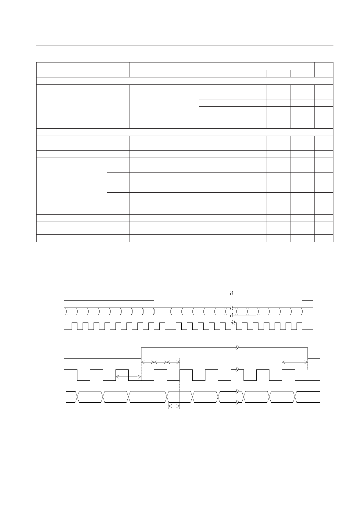
Control Timing and Data Format
To control the LC75412E and LC75412W input specified serial data to the CE, CL, and DI pins.
The data configuration consists of a total of 52 bits broken down into 8 address bits and 44 data bits.
CE
DI
D43 D42 D41 D40 D39 D38 D5 D4 D3 D2 D0 D1 A3 A2 A1 A0 B3 B2 B1 B0
CL
1µs
min
1µs
min
1µs min ≤ T
DEST
1µs
min
1µs
min
1µs
min
CE
DI
CL
Page 6
Address code (B0 to A3)
The LC75412E and 75412W use 8-bit address code and can be used in common with ICs that support SANYO’s CCB
serial bus.
Address Code
(LSB) (81HEX)
Control code allocation
Input Switching Control
No. 7053-6/21
LC75412E, 75412W
B0 B1 B2 B3 A0 A1 A2 A3
1 0 0 0 0 0 0 1
D0 D1 D2 Setting Setting
0 0 0 L1 (R1)
1 0 0 L2 (R2)
0 1 0 L3 (R3)
1 1 0 L4 (R4)
0 0 1 L5 (R5)
1 0 1 L6 (R6)
D3 Bit for IC testing: Normally set to 0
Input Gain Control
D4 D5 D6 D7 Operation
0 0 0 0 0dB
1 0 0 0 +1.25dB
0 1 0 0 +2.50dB
1 1 0 0 +3.75dB
0 0 1 0 +5.00dB
1 0 1 0 +6.25dB
0 1 1 0 +7.50dB
1 1 1 0 +8.75dB
0 0 0 1 +10.0dB
1 0 0 1 +11.25dB
0 1 0 1 +12.5dB
1 1 0 1 +13.75dB
0 0 1 1 +15.0dB
1 0 1 1 +16.25dB
0 1 1 1 +17.5dB
1 1 1 1 +18.75dB
Page 7
No. 7053-7/21
LC75412E, 75412W
Volume Control (0 to –40dB)
D8 D9 D10 D11 D12 D13 D14 D15 Operation
0 0 0 0 0 0 0 0 0dB
1 0 0 0 0 0 0 0 –1dB
0 1 0 0 0 0 0 0 –2dB
1 1 0 0 0 0 0 0 –3dB
0 0 1 0 0 0 0 0 –4dB
1 0 1 0 0 0 0 0 –5dB
0 1 1 0 0 0 0 0 –6dB
1 1 1 0 0 0 0 0 –7dB
0 0 0 1 0 0 0 0 –8dB
1 0 0 1 0 0 0 0 –9dB
0 1 0 1 0 0 0 0 –10dB
1 1 0 1 0 0 0 0 –11dB
0 0 1 1 0 0 0 0 –12dB
1 0 1 1 0 0 0 0 –13dB
0 1 1 1 0 0 0 0 –14dB
1 1 1 1 0 0 0 0 –15dB
0 0 0 0 1 0 0 0 –16dB
1 0 0 0 1 0 0 0 –17dB
0 1 0 0 1 0 0 0 –18dB
1 1 0 0 1 0 0 0 –19dB
0 0 1 0 1 0 0 0 –20dB
1 0 1 0 1 0 0 0 –21dB
0 1 1 0 1 0 0 0 –22dB
1 1 1 0 1 0 0 0 –23dB
0 0 0 1 1 0 0 0 –24dB
1 0 0 1 1 0 0 0 –25dB
0 1 0 1 1 0 0 0 –26dB
1 1 0 1 1 0 0 0 –27dB
0 0 1 1 1 0 0 0 –28dB
1 0 1 1 1 0 0 0 –29dB
0 1 1 1 1 0 0 0 –30dB
1 1 1 1 1 0 0 0 –31dB
0 0 0 0 0 1 0 0 –32dB
1 0 0 0 0 1 0 0 –33dB
0 1 0 0 0 1 0 0 –34dB
1 1 0 0 0 1 0 0 –35dB
0 0 1 0 0 1 0 0 –36dB
1 0 1 0 0 1 0 0 –37dB
0 1 1 0 0 1 0 0 –38dB
1 1 1 0 0 1 0 0 –39dB
0 0 0 1 0 1 0 0 –40dB
Page 8

No. 7053-8/21
LC75412E, 75412W
Volume Control (–41 to –∞dB)
D8 D9 D10 D11 D12 D13 D14 D15 Operation
1 0 0 1 0 1 0 0 –41dB
0 1 0 1 0 1 0 0 –42dB
1 1 0 1 0 1 0 0 –43dB
0 0 1 1 0 1 0 0 –44dB
1 0 1 1 0 1 0 0 –45dB
0 1 1 1 0 1 0 0 –46dB
1 1 1 1 0 1 0 0 –47dB
0 0 0 0 1 1 0 0 –48dB
1 0 0 0 1 1 0 0 –49dB
0 1 0 0 1 1 0 0 –50dB
1 1 0 0 1 1 0 0 –51dB
0 0 1 0 1 1 0 0 –52dB
1 0 1 0 1 1 0 0 –53dB
0 1 1 0 1 1 0 0 –54dB
1 1 1 0 1 1 0 0 –55dB
0 0 0 1 1 1 0 0 –56dB
1 0 0 1 1 1 0 0 –57dB
0 1 0 1 1 1 0 0 –58dB
1 1 0 1 1 1 0 0 –59dB
0 0 1 1 1 1 0 0 –60dB
1 0 1 1 1 1 0 0 –61dB
0 1 1 1 1 1 0 0 –62dB
1 1 1 1 1 1 0 0 –63dB
0 0 0 0 0 0 1 0 –64dB
1 0 0 0 0 0 1 0 –65dB
0 1 0 0 0 0 1 0 –66dB
1 1 0 0 0 0 1 0 –67dB
0 0 1 0 0 0 1 0 –68dB
1 0 1 0 0 0 1 0 –69dB
0 1 1 0 0 0 1 0 –70dB
1 1 1 0 0 0 1 0 –71dB
0 0 0 1 0 0 1 0 –72dB
1 0 0 1 0 0 1 0 –73dB
0 1 0 1 0 0 1 0 –74dB
1 1 0 1 0 0 1 0 –75dB
0 0 1 1 0 0 1 0 –76dB
1 0 1 1 0 0 1 0 –77dB
0 1 1 1 0 0 1 0 –78dB
1 1 1 1 0 0 1 0 –79dB
1 1 1 1 1 1 0 –∞
Page 9

No. 7053-9/21
LC75412E, 75412W
Tone Control
D16 D17 D18 D19 D40 Bass
D24 D25 D26 D27 D41 Treble
1 1 0 0 1 +18dB
0 1 0 0 1 +16dB
1 0 0 0 1 +14dB
0 1 1 0 0 +12dB
1 0 1 0 0 +10dB
0 0 1 0 0 +8dB
1 1 0 0 0 +6dB
0 1 0 0 0 +4dB
1 0 0 0 0 +2dB
0 0 0 0 0 0dB
1 0 0 1 0 –2dB
0 1 0 1 0 –4dB
1 1 0 1 0 –6dB
0 0 1 1 0 –8dB
1 0 1 1 0 –10dB
0 1 1 1 0 –12dB
1 0 0 1 1 –14dB
0 1 0 1 1 –16dB
1 1 0 1 1 –18dB
Fader Volume Control
D28 D29 D30 D31 Operation
0 0 0 0 0dB
1 0 0 0 –1dB
0 1 0 0 –2dB
1 1 0 0 –4dB
0 0 1 0 –6dB
1 0 1 0 –8dB
0 1 1 0 –10dB
1 1 1 0 –12dB
0 0 0 1 –14dB
1 0 0 1 –16dB
0 1 0 1 –18dB
1 1 0 1 –20dB
0 0 1 1 –30dB
1 0 1 1 –45dB
0 1 1 1 –60dB
1 1 1 1 –∞
Channel Selection Control
D32 D33 Operation
0 0
1 0 RCH
0 1 LCH
1 1 L/R simultaneously
D20 D21 D22 D23
0 0 0 0 Set to 0
Page 10

No. 7053-10/21
LC75412E, 75412W
Fader Rear/Front Control
D34 Setting
0 Rear
1 Front
Loudness Control
D35 Setting
0 OFF
1 ON
Test Mode Control
D42 D43 Setting
0 0 For IC testing. Always set to 0.
Zero-Cross Control
D36 D37 Setting
0 0 Data write through zero-cross detection
1 1 Zero-cross detection stopped (data write at falling edge of CE)
Zero-Cross Signal Detection Block Control
D38 D39 Setting
0 0 Selector
1 0 Volume
0 1 Tone
1 1 Fader
Page 11

No. 7053-11/21
LC75412E, 75412W
Pin Functions
Pin Name Pin No. Function Equivalent circuit
• Single-end input pins
L1
L2
L3
L4
L6
R1
R2
R3
R4
R6
54
53
52
51
55
59
60
61
62
58
VDD
LVref
RVref
• Input selector output pins
LSEL0
RSEL0
48
1
VDD
• Volume and equalizer input pins.
LVRIN
RVRIN
47
2
VDD
• Loudness pins. Connect high-pass compensation RC between
LCT (RCT) and LVRIN (RVRIN), and connect low-pass
compensation RC between LCT (RCT) and GND.
LCT
RCT
46
3
VDD
Continued on next page.
LVref
RVref
VDD
VDD
+
–
M
P
• Differential input pins
50
49
63
64
L5M
L5P
R5M
R5P
Page 12

No. 7053-12/21
LC75412E, 75412W
Continued from preceding page.
Pin Name Pin No. Function Equivalent circuit
Continued on next page.
• Equalizer F1 band filter configuration capacitor connection pins.
Connect capacitor between
LF1C1 (RF1C1) and LF1C2 (RF1C2)
LF1C2 (RF1C2) and LF1C3 (RF1C3)
LF1C1
LF1C2
LF1C3
RF1C1
RF1C2
RF1C3
42
41
40
7
8
9
VDD
FnC1
VDD
VDD
FnC3
VDD
FnC2
+
–
• Equalizer F3 band filter configuration capacitor connection pins.
Connect capacitor between
LF3C1 (RF3C1) and LF3C2 (RF3C2)
LF3C2 (RF3C2) and LF3C3 (RF3C3)
LF3C1
LF3C2
LF3C3
RF3C1
RF3C2
RF3C3
36
35
34
13
14
15
• Equalizer output pins
LTOUT
RTOUT
33
16
VDD
• Fader block input pins
• Drive at low impedance.
LFIN
RFIN
32
17
VDD
• No connect pin
NC
NC
NC
NC
NC
NC
NC
NC
NC
NC
NC
NC
NC
45
44
43
39
38
37
21
10
11
12
5
4
3
• Dedicated IC test pin.
• Normally this pin is used connected to GND.
TEST 28
VDD
Page 13

No. 7053-13/21
LC75412E, 75412W
Pin Name Pin No. Function Equivalent circuit
Continued from preceding page.
• Fader output pins. Attenuation is possible separately for the front
end and rear end. The attenuation amount is the same for L and
R.
LFOUT
LROUT
RFOUT
RROUT
31
30
18
19
VDD
• Connect a capacitor of a few tens of µF between Vref and AVSS
(VSS) as a VDD/2 voltage generator, current ripple
countermeasure.
Vref 57
VDD
LVref
RVref
• External muting control pin
• Setting this pin to V
SS
level sets forcibly fader volume block to
–∞ level.
MUTE 23
VDD
• Timer pin when there is no signal in the zero-cross circuit.
Forcibly set data when there is no zero-cross signal, from the time
the data is set until the timer ends.
TIM 20
VDD
• Input pin for serial data and clock used for control
CL
DI
26
25
VDD
• Chip enable pin. Data is written to the internal latch and the analog
switches are operated when the level changes from High to Low.
Data transfer is enabled when the level is High.
CE 24
• Analog system ground pins
LAVSS
RAVSS
29
22
• Power supply pinVDD 56
• Logic system ground pinDVSS 27
Page 14

Internal Equivalent Circuit Block Diagram
Selector Block Equivalent Circuit Block Diagram
No. 7053-14/21
LC75412E, 75412W
1.25dB
2.50dB
3.75dB
5.00dB
6.25dB
7.50dB
8.75dB
LSELO
0dB
+
-
50k
50k
50k
+
-
LVref
6.702k
5.804k
5.026k
4.352k
3.769k
3.264k
2.826k
2.447k
2.119k
1.835k
1.589k
1.376k
1.192k
1.032k
0.894k
5.774k
LVref
10.0dB
11.25dB
12.5dB
13.75dB
15.0dB
16.25dB
17.5dB
18.75dB
L3
LVref
LVref
LVref
INMUTE SW
L2
L1
50k
LVref
L4
R4=25k
R1=22.65k
R2=25k
R3=22.65k
LVref
L5P
L5M
50k
L6
Total resistance: 50 kΩ
Same for right channel
Unit (Resistance: Ω)
LVref
Page 15

Volume Block Equivalent Circuit Block Diagram
No. 7053-15/21
LC75412E, 75412W
R1=5434
LVRIN
1236
R85
LVref
1233
R84
1227
R82
1230
R83
1500
R81
1M
R86
LCT
R2=4845
R3=4319
R4=3850
R5=3431
–1dB
–2dB
–3dB
–4dB
–5dB
–6dB
–7dB
0dB
–8dB
–9dB
–10dB
–11dB
–12dB
–13dB
–14dB
–15dB
–16dB
–17dB
–18dB
–19dB
–20dB
–21dB
–22dB
–23dB
–24dB
–25dB
–26dB
–27dB
R6=3058
R7=2726
R8=2429
R9=2165
R10=1930
R11=1720
R12=1533
R13=1366
R14=1218
R15=1085
R16=967
R17=862
R18=768
R19=685
R20=610
R21=544
R22=485
R23=432
R24=385
R25=343
R26=306
R27=273
R28=243
R29=216
R30=193
R31=172
R32=153
–28dB
–29dB
–30dB
–31dB
–32dB
–33dB
–34dB
–35dB
–36dB
–37dB
–38dB
–39dB
–40dB
–41dB
–42dB
–43dB
–44dB
–45dB
–46dB
–47dB
–48dB
–49dB
–50dB
–51dB
–52dB
–53dB
–54dB
R33=839
R34=748
R35=667
R36=594
R37=530
R38=472
R39=421
R40=375
R41=334
R42=298
R43=266
R44=237
R45=211
R46=188
R47=168
R48=149
R49=133
R50=119
R51=106
R52=94
R53=84
R54=75
R55=133
R56=119
R57=106
R58=94
R59=84
–55dB
–56dB
–57dB
–58dB
–59dB
–60dB
–61dB
–62dB
–63dB
–64dB
–65dB
–66dB
–67dB
–68dB
–69dB
–70dB
–71dB
–72dB
–73dB
–74dB
–75dB
–76dB
–77dB
–78dB
–79dB
– ∞
R60=75
R61=134
R62=119
R63=106
R64=95
R65=84
R66=75
R67=134
R68=119
R69=106
R70=95
R71=85
R72=75
R73=134
R74=120
R75=107
R76=95
R77=85
R78=76
R79=67
R80=552
Total resistance of
48.746 kΩ over tap
Total resistance of
1.256 kΩ under tap
(LOUD OFF)
Total resistance of
7.662 kΩ under tap
(LOUD ON)
Same for right channel
Unit (Resistance: Ω)
To tone block
Page 16

Tone Control Block Equivalent Circuit Diagram
No. 7053-16/21
LC75412E, 75412W
SW3
SW4
LF3C1
SW1
SW2 SW3
SW4
LTOUT
18dB
16dB
14dB
12dB
10dB
LF1C1
8dB
6dB
4dB
2dB
0dB
SW1
SW2
2.189
2.756
3.470
4.368
5.498
6.923
8.715
10.972
13.813
0.655
18dB
16dB
14dB
12dB
10dB
8dB
6dB
4dB
2dB
0dB
2.189
2.756
3.470
4.368
5.498
6.923
8.715
10.972
13.813
0.655
LF1C2 LF1C3 LF3C3
3.90
LF3C2
3.90
+
–
+
–
+
–
Unit: kΩ
Total resistance: 59.359 kΩ
Same for right channel
During boost, SW 1 and SW 3 are ON, during cut SW 2 and SW 4 are ON,
and when 0 dB, 0 dB SW and SW 2 and SW 3 are ON.
Page 17

– R1 ÷ 2 = 3900 Ω
R3 =
10
G/20
– 1
R2
F1/F3 Band Circuit
The equivalent circuit and the formula for calculating the external RC with a mean frequency of 1 kHz are shown below.
• F1/F3 band equivalent circuit block diagram
1. Calculate R3 with G
+18 dB
= 18 dB:
2. Calculate C with the center frequency f0 = 1 kHz
No. 7053-17/21
LC75412E, 75412W
• Calculation example
Specification Mean frequency: f0 = 1 kHz
Gain during maximum boost: G
+18 dB
= 18 dB
Let us use R1 = 0.665 kΩ, R2 = 58.704 kΩ, and C1 = C2 = C.
R1 R2
R3
C2C1
2
1
0
(R1+R2)R3C1C2
f
π
=
0.01 µF
39359×390010002
1
(R1+R2)R3f02
1
ππ
≅
×
= = 0.010 × 10–6 =C
3. Calculate Q:
1.789
R3(R1+R2)
(R1+R2)R3 (2R3+R1)
1
≅
×
=Q
1 + G
+18 dB
= 20 × LOG
10
2R3+R1
R2
Page 18

Fader Volume Block Equivalent Circuit Block Diagram
No. 7053-18/21
LC75412E, 75412W
LFIN
5.437k
When FADER = "1", S2 and S3 are ON.
When FADER = "0", S1 and S4 are ON.
Unit: Ω
Total resistance: 50 kΩ
Same for right channel
4.846k
8.169k
4.094k
LFOUT
LVref
–1dB
–2dB
0dB
S1
S2
S3
S4
6.489k
5.154k
–6dB
–8dB
–4dB
3.252k
2.583k
2.052k
3.419k
–12dB
–14dB
–10dB
1.630k
1.295k
–18dB
–20dB
–16dB
1.300k
0.231k
–45dB
–60dB
–∞dB
–30dB
0.050k
LROUT
When –∞ data is sent to the main volume, S1 and S2
become open, and S3 and S4 simultaneously become ON.
Page 19

Usage Cautions
(1) Data transmission at power ON
• The status of internal analog switches is unstable at power ON. Therefore, perform muting or some other
countermeasure until the data has been set.
(2) Description of zero-cross switching circuit operation
The LC75412E and 75412W have a function to switch zero-cross comparator signal detection locations, enabling the
selection of the optimum detection location for blocks whose data is to be updated. Basically, the switching noise can
be minimized by inputting the signal immediately following the block whose data is to be updated to the zero-cross
comparator, so it is necessary to switch the detection location every time.
LC75412E, 75412W Zero-Cross Detection Circuit
No. 7053-19/21
LC75412E, 75412W
Volume Tone
Switch
Fader
Zero-cross
comparator
Selector
(3) Zero-cross switching control method
The zero-cross switching control method consists of setting the zero-cross control bits to the zero-cross detection
mode (D36, D37 = 0), and specifying the detection blocks (D38, D39) before transmitting the data. These control bits
are latched immediately following data transfer, that is to say beforehand in sync with the falling edge of CE, so when
updating data of volumes, etc., it is possible to perform mode setting and zero-cross switching with one data transfer.
An example of control when updating the data of the volume block is shown below.
Zero-cross detection
mode setting
Volume block
setting
D36 D37 D38 D39
0 0 1 0
(4) Zero-cross timer setting
If the input signal becomes lower than the zero-cross comparator detection sensitivity, or if only low-frequency
signals are input, zero-cross detection continues to be impossible, and data is not latched during this time.
The zero-cross timer can set a time for forcible latch during such a status when zero-cross detection is not possible.
For example, to set 25 ms,
using T = 0.69CR and C = 0.033 µF,
we obtain
Normally, a value between 10 ms and 50 ms is set.
R=
1.1 MΩ
25 ×10
–3
0.69 × 0.033 × 10
–6
Page 20

No. 7053-20/21
LC75412E, 75412W
(5) Cautions related to serial data transfer
1. To ensure that the high-frequency digital signals transferred to the CL, DI, and CE pins do not spill over to the
analog signal block, either guard these signal lines with a ground pattern, or perform transmission using shielded
wires.
2. The data format of the LC75412E and 75412W uses 8-bit addresses and 44-bit data. When sending data using
multiples of 8 (when sending 48 bits), use the method described in Figure 1.
Method for Receiving Data Using Multiple of 8 of LC75412E and 75412W
Figure 1
D43D42D41D40D39D38D37D36D3D2D1D0XXXX
Test mode control
Input switching controlDummy data
X : don’t care
(6) Note on usage of external muting
When using external mute function, take adequate countermeasures against noise to prevent malfunction.
Input Gain Step Characteristics
Level — dB
ILC05454
0
5
10
15
20
0 2 4 1086 12 14 16 18 20
V
DD
= 9 V
V
IN
= –20 dBV
f = 1 kHz
Overall
20 kHz
1 kHz
Output Level Characteristics
Level — dB
Frequency, f — HzStep setting
ILC05455
--60
10
--10
--30
--20
--40
--50
0
10 100 10k1k
V
DD
= 9 V, V
IN
= 0, V
R
= 0 to –54 dB
Overall
2 3 5 7 2 3 5 7 2 3 5 7 2 3 5
100k
7
Loudness Characteristics
Level — dB
Frequency, f — Hz
ILC05456
--60
10
--10
--30
--20
--40
--50
0
V
DD
= 9 V, V
IN
= 0, V
R
= 0 to –54 dB
Loudness ON, Overall
100k10 100 10k1k
2 3 5 7 2 3 5 7 2 3 5 7 2 3 5 7
Feder Step Characteristics
Level — dB
Step setting — dB
ILC05457
--100
--90
--80
--70
--60
--50
--40
--30
--20
--10
0
--∞ --70 --60 --50 --40 --30 --20 --10 0
V
DD
= 9 V
V
IN
= 0
f = 1 kHz
Overall
f = 20 kHz
f = 1 kHz
Page 21

PS No. 7053-21/21
LC75412E, 75412W
This catalog provides information as of Octomber, 2001. Specifications and information herein are subject
to change without notice.
Specifications of any and all SANYO products described or contained herein stipulate the performance,
characteristics, and functions of the described products in the independent state, and are not guarantees
of the performance, characteristics, and functions of the described products as mounted in the customer’s
products or equipment. To verify symptoms and states that cannot be evaluated in an independent device,
the customer should always evaluate and test devices mounted in the customer’s products or equipment.
SANYO Electric Co., Ltd. strives to supply high-quality high-reliability products. However, any and all
semiconductor products fail with some probability. It is possible that these probabilistic failures could
give rise to accidents or events that could endanger human lives, that could give rise to smoke or fire,
or that could cause damage to other property. When designing equipment, adopt safety measures so
that these kinds of accidents or events cannot occur. Such measures include but are not limited to protective
circuits and error prevention circuits for safe design, redundant design, and structural design.
In the event that any or all SANYO products (including technical data, services) described or contained
herein are controlled under any of applicable local export control laws and regulations, such products must
not be exported without obtaining the export license from the authorities concerned in accordance with the
above law.
No part of this publication may be reproduced or transmitted in any form or by any means, electronic or
mechanical, including photocopying and recording, or any information storage or retrieval system,
or otherwise, without the prior written permission of SANYO Electric Co., Ltd.
Any and all information described or contained herein are subject to change without notice due to
product/technology improvement, etc. When designing equipment, refer to the “Delivery Specification”
for the SANYO product that you intend to use.
Information (including circuit diagrams and circuit parameters) herein is for example only; it is not
guaranteed for volume production. SANYO believes information herein is accurate and reliable, but
no guarantees are made or implied regarding its use or any infringements of intellectual property rights
or other rights of third parties.
0
--5
--10
--15
--20
Level — dB
--25
--30
--35
--40
1.0
7
5
3
2
0.1
7
5
3
2
0.01
7
5
3
Total harmonic distortion, THD — %
2
0.001
10
F1 Band Characteristics
V
= 9 V
DD
= –20 dBV
V
IN
Overall
2 3 5 7
2 3 5 7
10010
Frequency, f — Hz
1k
2 3 5 7
10k
2 3 5 7
THD — Frequency Characteristics
V
= 9 V
DD
80 kHz LPF
Overall
= 0 dBV
V
IN
= –10 dBV
V
IN
2 3
75 2 31k75 2 3
100
Frequency, f — Hz
75 2 3
10k
ILC05458
75
ILC05460
100k
100k
0
V
DD
V
IN
--5
Overall
--10
--15
--20
Level — dB
--25
--30
--35
--40
1.0
V
7
5
80 kHz LPF
3
Overall
2
0.1
7
5
3
2
0.01
7
5
3
Total harmonic distortion, THD — %
2
0.001
--40 --35 --30 --25 --20 --15 --10 --5 0 5
F3 Band Characteristics
= 9 V
= –20 dBV
2 3 5 7
2 3 5 7
10010
Frequency, f — Hz
1k
2 3 5 7
10k
THD — Input Level Characteristics
= 9 V
DD
20 kHz
10 kHz
Input level — dBV
2 3 5 7
ILC05459
1 kHz
ILC05461
100k
 Loading...