

Page 1
Specifications
Absolute Maximum Ratings at Ta = 25°C, VSS= 0 V
CMOS LSI
Ordering number : EN5056A
63096HA (OT)/71895HA (OT) No. 5056-1/17
SANYO Electric Co.,Ltd. Semiconductor Bussiness Headquarters
TOKYO OFFICE Tokyo Bldg., 1-10, 1 Chome, Ueno, Taito-ku, TOKYO, 110 JAPAN
Single-Chip Electronic Volume Control System
LC75395E
Overview
The LC75395E is an electronic volume control that
provides volume, balance, five-band equalization and
input switching functions. These functions are controlled
from serial input data.
Functions
• Volume control: The volume control provides 25
attenuation positions: from 0 dB to –17.5 dB in 1.25 dB
steps, from –17.5 dB to –25 dB in 2.5 dB steps, from
–25 dB to –36.25 dB in 3.75 dB steps and with settings
for –41.25 dB, –50 dB, –60 dB and –∞.
A balance function can be implemented by controlling
the left and right channels independently.
• Equalizer: The equalizer function supports ±10 dB
control in 2 dB steps in each of the five bands. Of the
five bands, four provide peaking characteristics, and one
provides shelving characteristics.
• Selector: The selector function selects one of four inputs
for each of the left and right channels. An arbitrary
amplification level can be set for each input signal using
external components.
• Serial data input: All controls can be set from serial
input data (CCB format)
Features
• On-chip buffer amplifiers to minimize the number of
external components
• Silicon-gate CMOS process for minimal switching noise
• On-chip circuit to generate the VDD/2 reference voltage
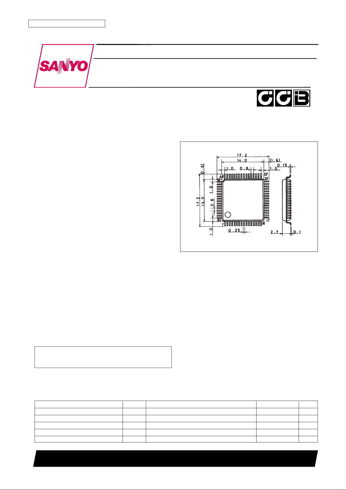
Package Dimensions
unit: mm
3159-QFP64E
• CCB is a trademark of SANYO ELECTRIC CO., LTD.
• CCB is SANYO’s original bus format and all the bus
addresses are controlled by SANYO.
Parameter Symbol Conditions Ratings Unit
Maximum supply voltage V
DD
max V
DD
12 V
Maximum input voltage V
IN
max CL, DI, CE, L1 to L4, R1 to R4, LTIN, RTIN, LVRIN, RVRIN VSS– 0.3 to VDD+ 0.3 V
Allowable power dissipation Pd max Ta ≤ 85°C 310 mW
Operating temperature Topr –30 to +85 °C
Storage temperature Tstg –40 to +125 °C
[LC75395E]
SANYO: QIP64E
Page 2
Allowable Operating Ranges at Ta = 25°C, VSS= 0 V
Electrical Characteristics at Ta = 25°C, VDD= 10 V, VSS= 0 V
Input Amplifier Characteristics at Ta = 25°C, VDD– VSS= 10 V
No. 5056-2/17
LC75395E
Parameter Symbol Conditions min typ max Unit
Supply voltage V
DD
V
DD
6.0 11.0 V
Input high level voltage V
IH
CL, DI, CE 4.0 V
DD
V
Input low level voltage V
IL
CL, DI, CE V
SS
1.0 V
Input voltage amplitude V
IN
CL, DI, CE, L1 to L4, R1 to R4, LTIN, RTIN,
V
SS
V
DD
Vp-p
LVRIN, RVRIN
Input pulse width t
øW
CL 1.0 µs
Setup time t
SETUP
CL, DI, CE 1.0 µs
Hold time t
HOLD
CL, DI, CE 1.0 µs
Operating frequency fopg CL 500 kHz
Parameter Symbol Conditions min typ max Unit
[Input Block]
Input resistance Rin L1 to L4, R1 to R4 1 MΩ
Clipping level Vcl LSELO, RSELO: THD = 1.0% 2.65 Vrms
Output load resistance R
L
LSELO, RSELO 3 kΩ
[Volume Control Block]
Input resistance Rin LVRIN, RVRIN 21 35 49 kΩ
[Equalizer Control Block]
Control range Geq Max, boost/cut ±8 ±10 ±12 dB
Step resolution Estep 1 2 3 dB
Internal feedback resistance Rfeed 17 28 39 kΩ
[Overall Characteristics]
Total harmonic distortion
THD (1) V
IN
= 1 Vrms, f = 1 kHz, with all controls flat overall 0.0033 %
THD (2) V
IN
= 1 Vrms, f = 20 kHz, with all controls flat overall 0.012 %
Crosstalk CT
V
IN
= 1 Vrms, f = 1 kHz, with all controls flat overall
86 dB
Rg = 1 kΩ
Output at maximum attenuation V
O
min
V
IN
= 1 Vrms, f = 1 kHz, with the main volume
–84 dB
control at –∞
V
N
(1) With all controls flat overall (IHF-A), Rg = 1 kΩ 3.9 µV
Output noise voltage
V
N
(2)
With all controls flat overall (DIN-AUDIO),
5.4 µV
Rg = 1 kΩ
Current drain I
DD
VDD– VSS= 11 V 25 33 mA
Input high level current I
IH
CL, DI, CE: VIN= 11 V 10 µA
Input low level current I
IL
CL, DI, CE: VIN= 0 V –10 µA
Parameter Symbol Conditions min typ max Unit
Input offset voltage V
IO
–10 +10 mV
Input offset current I
IO
VSS≤ VIN≤ V
DD
±10 nA
Open-loop voltage gain A
O
80 dB
0 dB bandwidth f
T
2.5 MHz
Allowable load resistance R
L
3 kΩ
Page 3
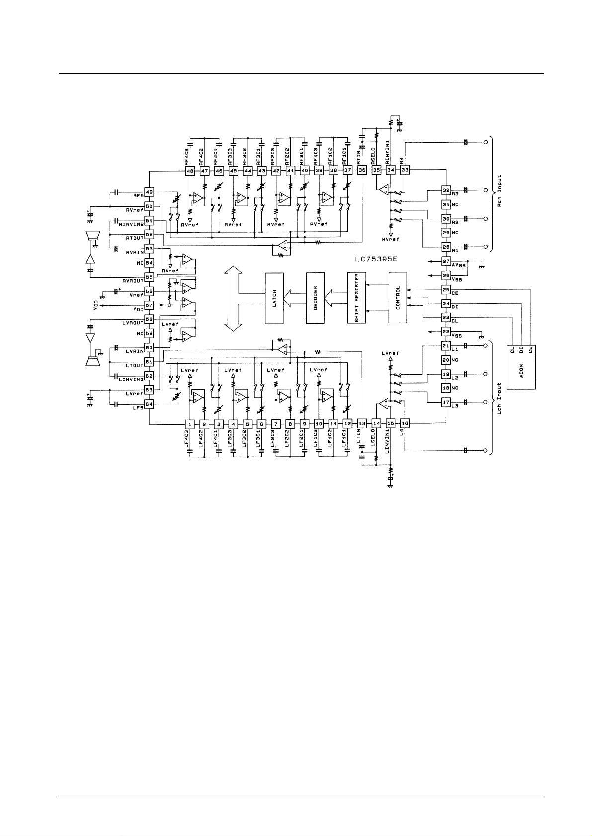
Equivalent Circuit Block Diagram and Sample Application Circuit
Note: If at all possible, use bipolar capacitors for all capacitors that do not have a polarity specified.
No. 5056-3/17
LC75395E
A03544
Page 4
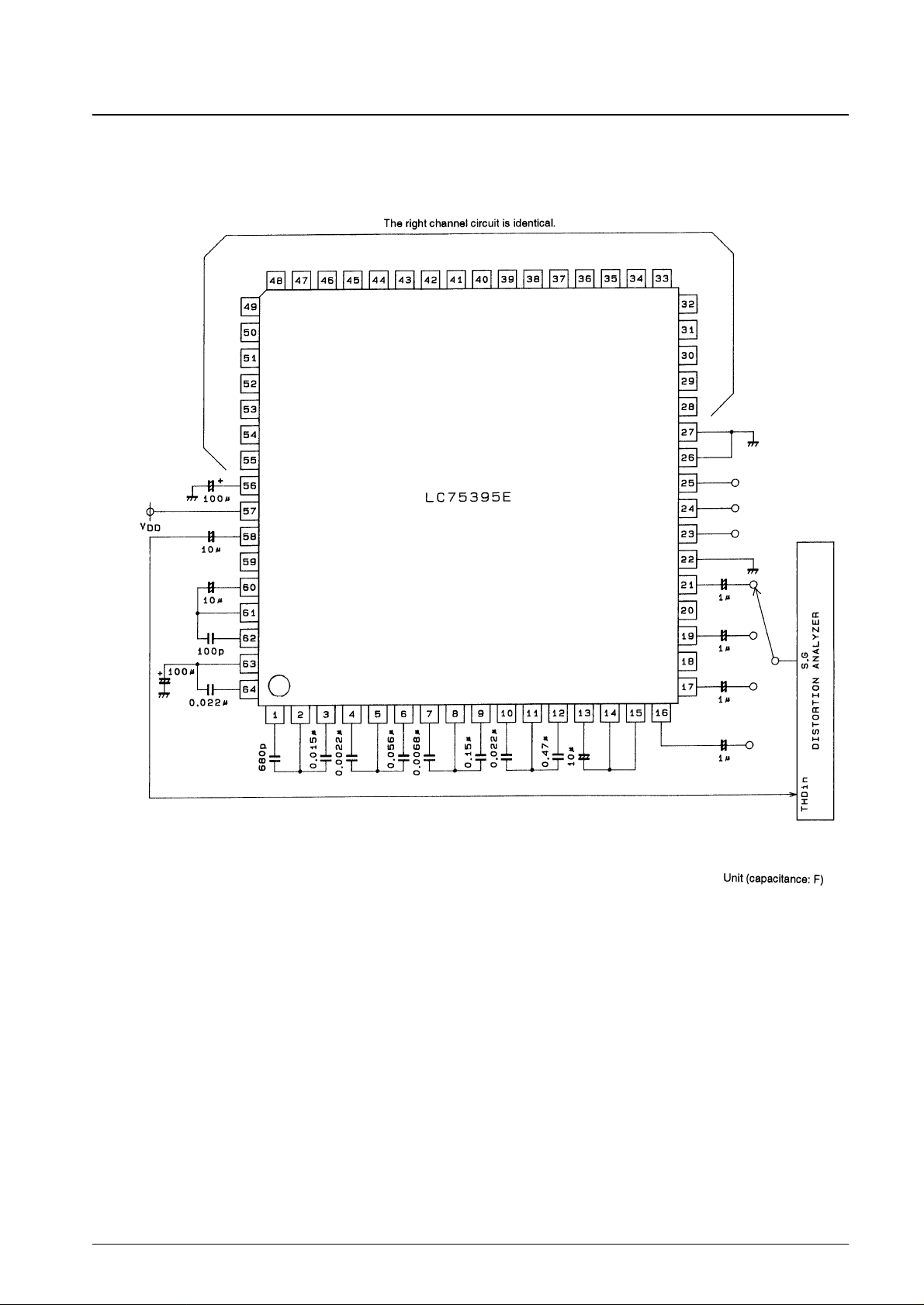
Test Circuits
1. Total Harmonic Distortion
No. 5056-4/17
LC75395E
A03545
Page 5
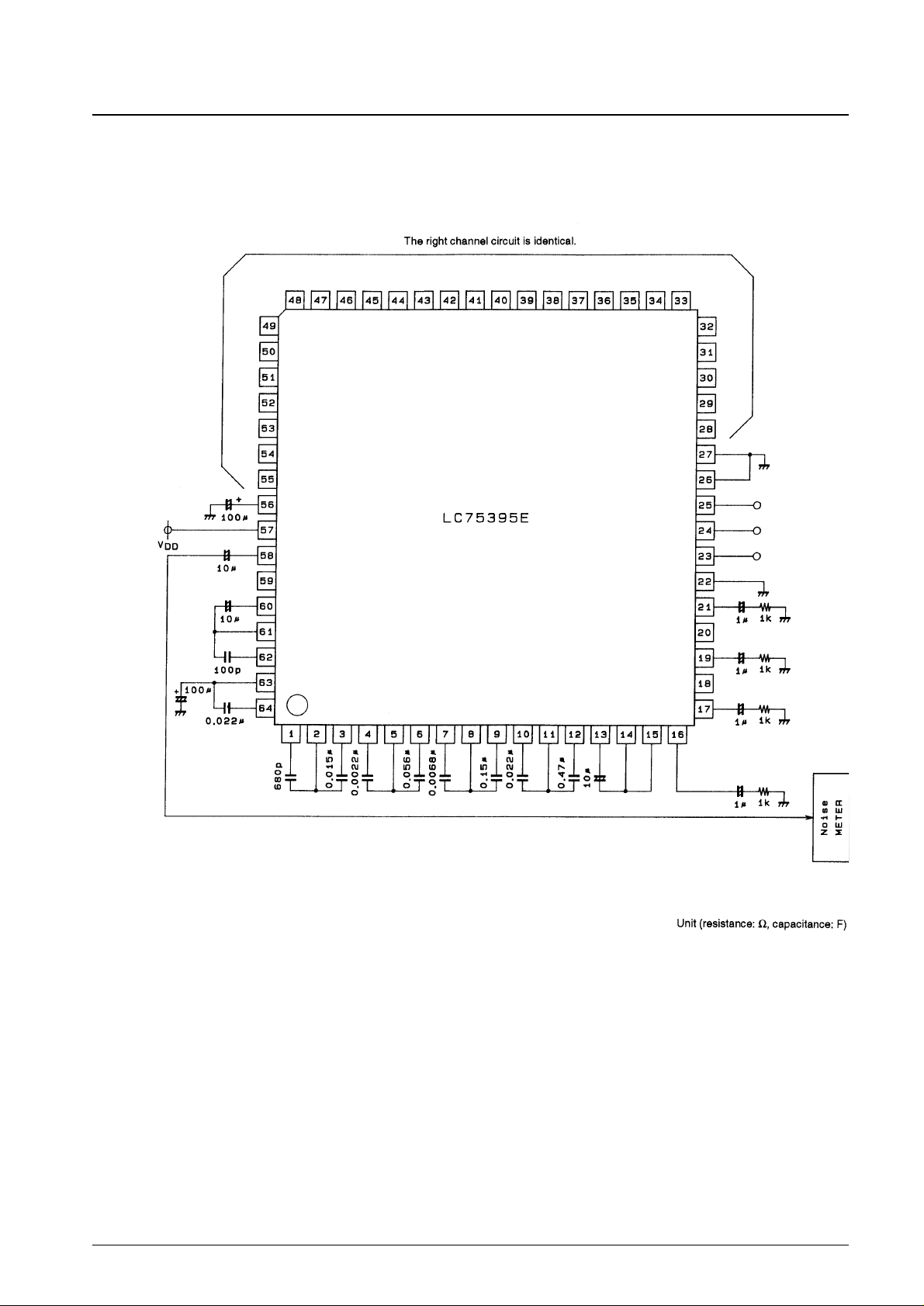
Test Circuits
2. Output Noise Voltage
No. 5056-5/17
LC75395E
A03546
Page 6
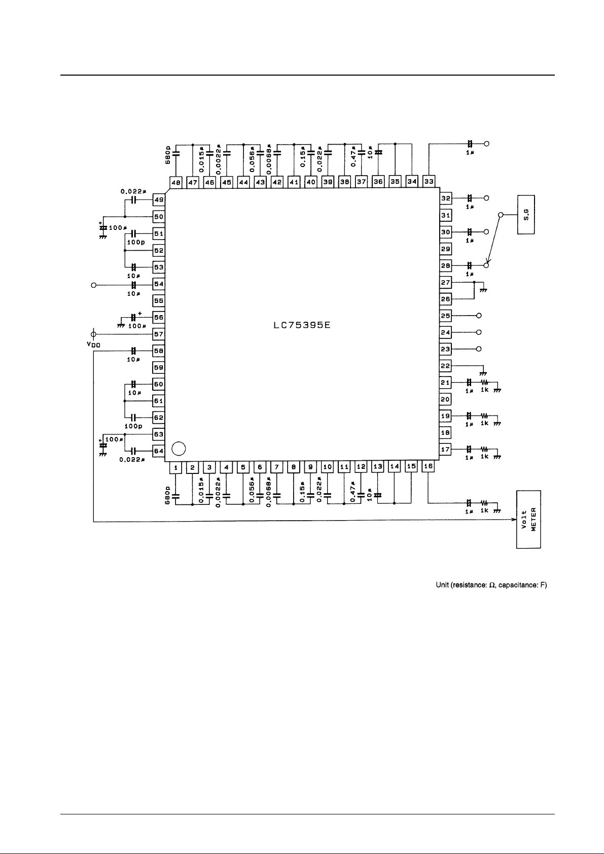
Test Circuits
3. Crosstalk
No. 5056-6/17
LC75395E
A03547
Page 7

Pin Assignment
No. 5056-7/17
LC75395E
A03548
Page 8

Pin Functions
No. 5056-8/17
LC75395E
Pin No. Symbol Function Note
12
11
10
37
38
39
9
8
7
40
41
42
6
5
4
43
44
45
3
2
1
46
47
48
13
36
14
35
64
49
21
19
17
16
28
30
32
33
57
22, 26
27
LF1C1
LF1C2
LF1C3
RF1C1
RF1C2
RF1C3
LF2C1
LF2C2
LF2C3
RF2C1
RF2C2
RF2C3
LF3C1
LF3C2
LF3C3
RF3C1
RF3C2
RF3C3
LF4C1
LF4C2
LF4C3
RF4C1
RF4C2
RF4C3
LTIN
RTIN
LSELO
RSELO
LF5
RF5
L1
L2
L3
L4
R1
R2
R3
R4
V
DD
V
SS
AV
SS
The left channel F1 band control block.
These are external capacitor connections.
The right channel F1 band control block.
These are external capacitor connections.
The left channel F2 band control block.
These are external capacitor connections.
The right channel F2 band control block.
These are external capacitor connections.
The left channel F3 band control block.
These are external capacitor connections.
The right channel F3 band control block.
These are external capacitor connections.
The left channel F4 band control block.
These are external capacitor connections.
The right channel F4 band control block.
These are external capacitor connections.
Tone control inputs
These must be driven by low-impedance circuits.
Input selector outputs
F5 band control block.
These are external capacitor connections.
Signal inputs
Power supply
Internal logic system ground
Internal operational amplifier ground
Continued on next page.
A03549
A03550
A03551
A03552
A03553
Page 9

Continued from preceding page.
No. 5056-9/17
LC75395E
Pin No. Symbol Function Note
56
63
50
15
34
62
51
61
52
60
53
58
55
25
24
23
18
20
29
31
54
59
Vref
LVref
RVref
LINVIN1
RINVIN1
LINVIN2
RINVIN2
LTOUT
RTOUT
LVRIN
RVRIN
LVROUT
RVROUT
CE
DI
CL
NC
NC
NC
NC
NC
NC
V
DD
/2 voltage generation block. A capacitor must be
inserted between Vref and V
SS
to suppress power supply
ripple.
Common pins for the volume control, tone control and
input switching blocks. Since capacitors inserted between
LVref (or RVref) and V
SS
become the residual resistance
when the volume control is set at maximum attenuation,
the values of these capacitors must be chosen carefully.
A voltage higher than V
DD
must never be applied.
Inverting inputs for the operational amplifiers that set the
input gain.
Inverting inputs for the graphic equalizer operational
amplifiers. Unnecessary frequency bands can be
excluded and oscillation prevented by inserting arbitrary
capacitors between the INVIN2 and TOUT pins.
Tone control outputs
Volume control inputs
These must be driven by low-impedance circuits.
Volume control outputs
Chip enable
Data is read into the internal latches and the analog
switches operate when this pin goes from high to low.
Data transfer is enabled when this pin is high.
Serial data and clock connections for chip control
Unused pins
A04449
A03555
A03556
A03557
A03558
A03559
A03560
A03561
Page 10

Input Block Internal Equivalent Circuit Diagram
Volume Control Block Internal Equivalent Circuit Diagram
No. 5056-10/17
LC75395E
A03562
A03563
Page 11

Equalizer Control Block Internal Equivalent Circuit (bands F1 to F4)
External Capacitor Calculations
The LC75395E supports four bands with peaking characteristics and one band with shelving characteristics.
1. Peaking Characteristics (bands F1 to F4)
The external capacitor functions as the structural element of a simulated inductor. The equivalent circuit and the
calculations required to achieve the desired center frequency are shown below.
• Equivalent circuit for the simulated inductor
No. 5056-11/17
LC75395E
A03564
A03565
Page 12

• Sample Calculation
Specifications 1) Center frequency FO= 107 Hz
2) Q at maximum boost: Q
+10 dB
= 0.8
➀ Derive the sharpness (QO) of the simulated inductor itself.
QO= (R1 + R4)/R1 × Q
+10 dB
≠ 4.270
➁ Derive C1.
C1 = 1/2πFOR1QO≠ 0.536 (µF)
➂ Derive C2.
C2 = QO/2πFOR2 ≠ 0.021 (µF)
• Sample values for C1 and C2
2. Shelving Characteristics (band F5)
To achieve ±10 dB (in 2 dB steps) at the target frequency, use an external capacitor C3 which has an impedance of
650 Ω.
No. 5056-12/17
LC75395E
Center frequency C1 C2
F
O
(Hz) (F) (F)
107 0.536 µ 0.021 µ
340 0.169 µ 6663 p
1070 0.054 µ 2117 p
3400 0.017 µ 666 p
Page 13

Control System Timing and Data Format
The LC75395E is controlled by inputting stipulated data to the CE, CL, and DI pins. The data consists of a total of 40
bits, of which 8 bits are address and 32 bits are data.
No. 5056-13/17
LC75395E
A03566
Page 14

No. 5056-14/17
LC75395E
A03730
A03731
Page 15

No. 5056-15/17
LC75395E
A03732
A03733
A03734
A03735
Page 16

No. 5056-16/17
LC75395E
Usage Notes
1. The states of the internal analog switches are undefined when power is first applied. Muting should be applied
externally until control data has been transferred and stored.
2. The signal lines for the CL, DI and CE pins should either be covered by the pattern ground or be formed from shielded
cable to prevent the high-frequency digital signals transmitted over these lines from entering the analog system.
A03736
A03737
A03738
A03739
Page 17

No. 5056-17/17
LC75395E
This catalog provides information as of November, 1997. Specifications and information herein are subject to
change without notice.
■ No products described or contained herein are intended for use in surgical implants, life-support systems, aerospace
equipment, nuclear power control systems, vehicles, disaster/crime-prevention equipment and the like, the failure of
which may directly or indirectly cause injury, death or property loss.
■ Anyone purchasing any products described or contained herein for an above-mentioned use shall:
➀ Accept full responsibility and indemnify and defend SANYO ELECTRIC CO., LTD., its affiliates, subsidiaries and
distributors and all their officers and employees, jointly and severally, against any and all claims and litigation and all
damages, cost and expenses associated with such use:
➁ Not impose any responsibility for any fault or negligence which may be cited in any such claim or litigation on
SANYO ELECTRIC CO., LTD., its affiliates, subsidiaries and distributors or any of their officers and employees
jointly or severally.
■ Information (including circuit diagrams and circuit parameters) herein is for example only; it is not guaranteed for
volume production. SANYO believes information herein is accurate and reliable, but no guarantees are made or implied
regarding its use or any infringements of intellectual property rights or other rights of third parties.
 Loading...