

Page 1
CMOS LSI
Ordering number :EN*5201A
LC75391, 75391M
SANYO Electric Co.,Ltd. Semiconductor Bussiness Headquarters
TOKYO OFFICE Tokyo Bldg., 1-10, 1 Chome, Ueno, Taito-ku, TOKYO, 110-8534 JAPAN
Single-Chip Electronic Volume Control System
N3095HA (OT) No. 5201-1/13
Overview
The LC75391 and LC75391M are single-chip electronic
volume and tone control systems that support volume
control, tone control, and input and output signal
switching functions controlled by serial input data.
Functions
• Input and output signal switching: The four I/O switches
can be set to on or off independently.
• Volume control: Independent control of the left and
right channels can be used to implement a balance
function.
0 to –20 dB in 2 dB steps, –20 to –32 dB in 3 dB steps,
–32 to –53 dB in 4 dB steps, –52 to –70 dB in 4.5 dB
steps, and –∞.
• Tone controls: Four frequency characteristic types
selectable by setting internal switches.
Also supports a buffer function that requires no external
components.
• Two general-purpose output ports: These ports allow
this LSI to control motorized volume controls and
general-purpose logic.
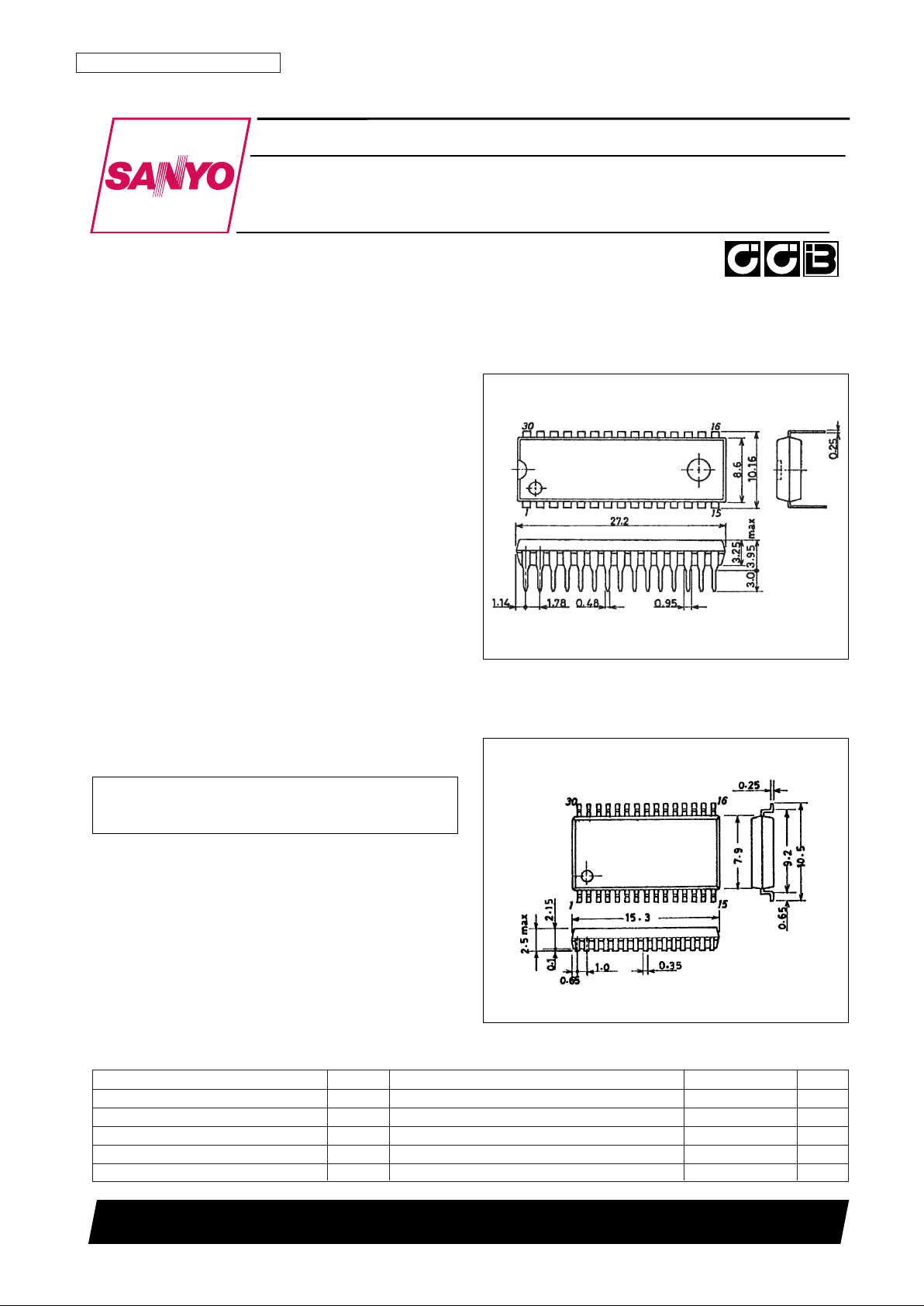
Package Dimensions
unit: mm
3196-DIP30SD
SANYO: DIP30SD
[LC75391]
• CCB is a trademark of SANYO ELECTRIC CO., LTD.
• CCB is SANYO’s original bus format and all the bus
addresses are controlled by SANYO.
unit: mm
3216-MFP30S
SANYO: MFP30S
[LC75391M]
Specifications
Absolute Maximum Ratings at Ta = 25°C, VSS= 0 V
Parameter Symbol Conditions Ratings Unit
Maximum supply voltage V
DD
max V
DD
12 V
Maximum input voltage V
IN
max CL, DI, CE, L1 to L4, R1 to R4 VSS– 0.3 to VDD+ 0.3 V
Allowable power dissipation Pd max Ta ≤ 85°C 160 mW
Operating temperature Topr –40 to +85 °C
Storage temperature Tstg –50 to +125 °C
Page 2
Allowable Operating Ranges at Ta = 25°C, VSS= 0 V
Electrical Characteristics at Ta = 25°C, VDD= 10 V, VSS= 0 V
No. 5201-2/13
LC75391, 75391M
Parameter Symbol Conditions min typ max Unit
Supply voltage V
DD
V
DD
5.5 11.0 V
Input high-level voltage V
IH
CL, DI, CE 4.0 V
DD
V
Input low-level voltage V
IL
CL, DI, CE V
SS
1.0 V
Output high-level voltage V
OH
PA, PB: IO= 5 mA VDD– 2 V
DD
V
Output low-level voltage V
OL
PA, PB: IO= 5 mA V
SS
2.0 V
Input voltage amplitude V
IN
L1 to L4, R1 to R4 V
SS
V
DD
Vp-p
Input pulse width t
øW
CL 1.0 µs
Setup time t
set up
CL, DI, CE 1.0 µs
Hold time t
hold
CL, DI, CE 1.0 µs
Operating frequency fopg CL 500 kHz
Parameter Symbol Conditions min typ max Unit
[Input Block]
Input resistance Rin L1 to L4, R1 to R4 500 kΩ
[Overall Characteristics]
THD (1)
V
IN
= 100 mVrms, f = 1 kHz, overall, buffer mode off,
0.013 %
Total harmonic distortion
flat state
THD (2)
V
IN
= 100 mVrms, f = 20 kHz, overall, buffer mode off,
0.013 %
flat state
Crosstalk CT
VIN= 1 Vrms, f = 1 kHz, overall, Rg = 1 kΩ,
81 dB
buffer mode off, flat state
Maximum attenuation V
O
min
V
IN
= 1 Vrms, f = 1 kHz, main volume at –∞,
–80 dB
buffer mode on
V
N
(1)
Flat overall (IHF-A), Rg = 1 kΩ, buffer mode off,
15 µV
Output noise voltage
flat state
V
N
(2)
Flat overall (DIN-AUDIO), Rg = 1 kΩ, buffer mode off,
22 µV
flat state
Current drain I
DD
VDD– VSS= 11 V 7 10 mA
Input high-level current I
IH
CL, DI, CE, VIN= 10 V 10 µA
Input low-level current I
IL
CL, DI, CE, VIN= 0 V –10 µA
Page 3
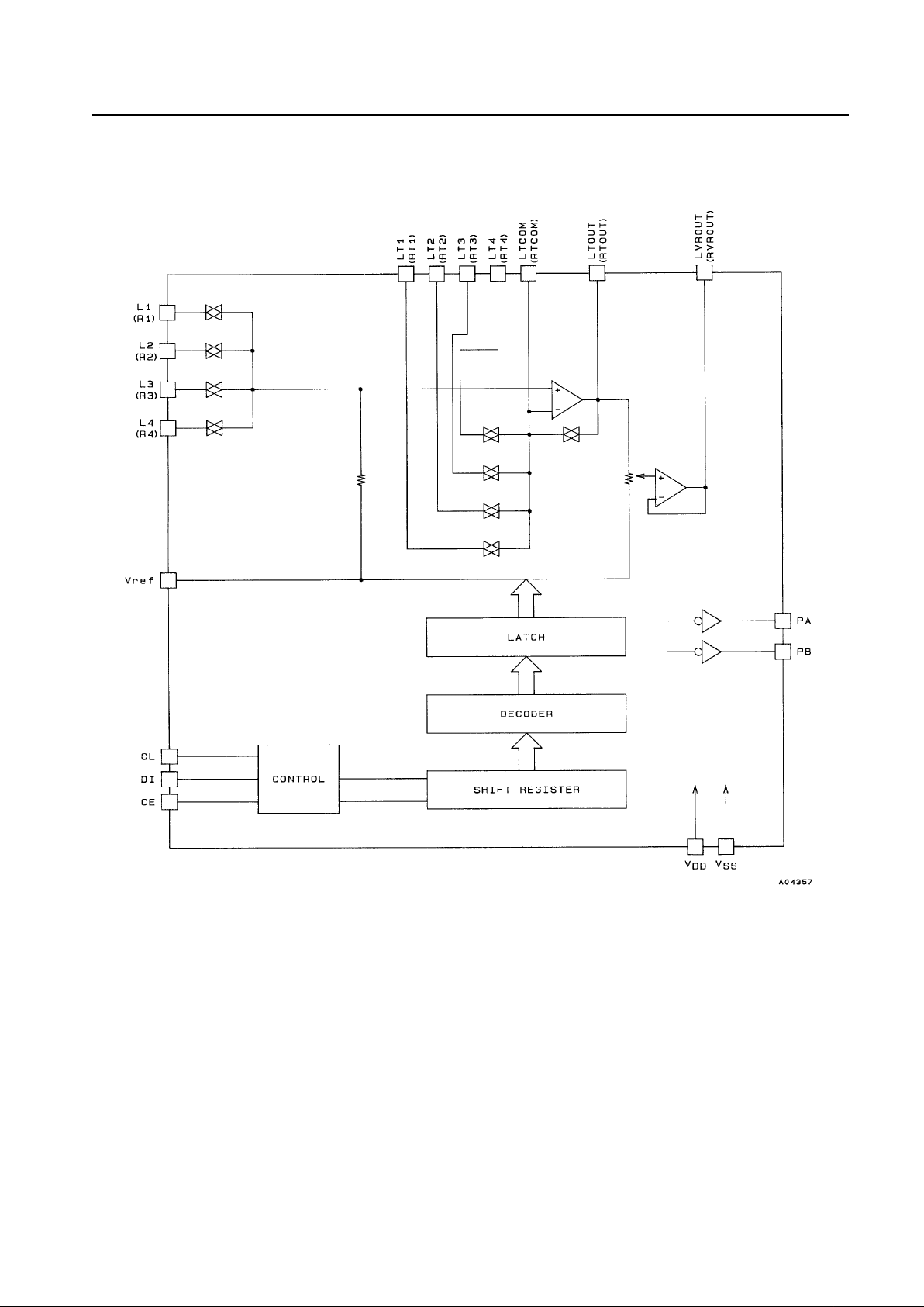
Equivalent Circuit Block Diagram
No. 5201-3/13
LC75391, 75391M
Page 4
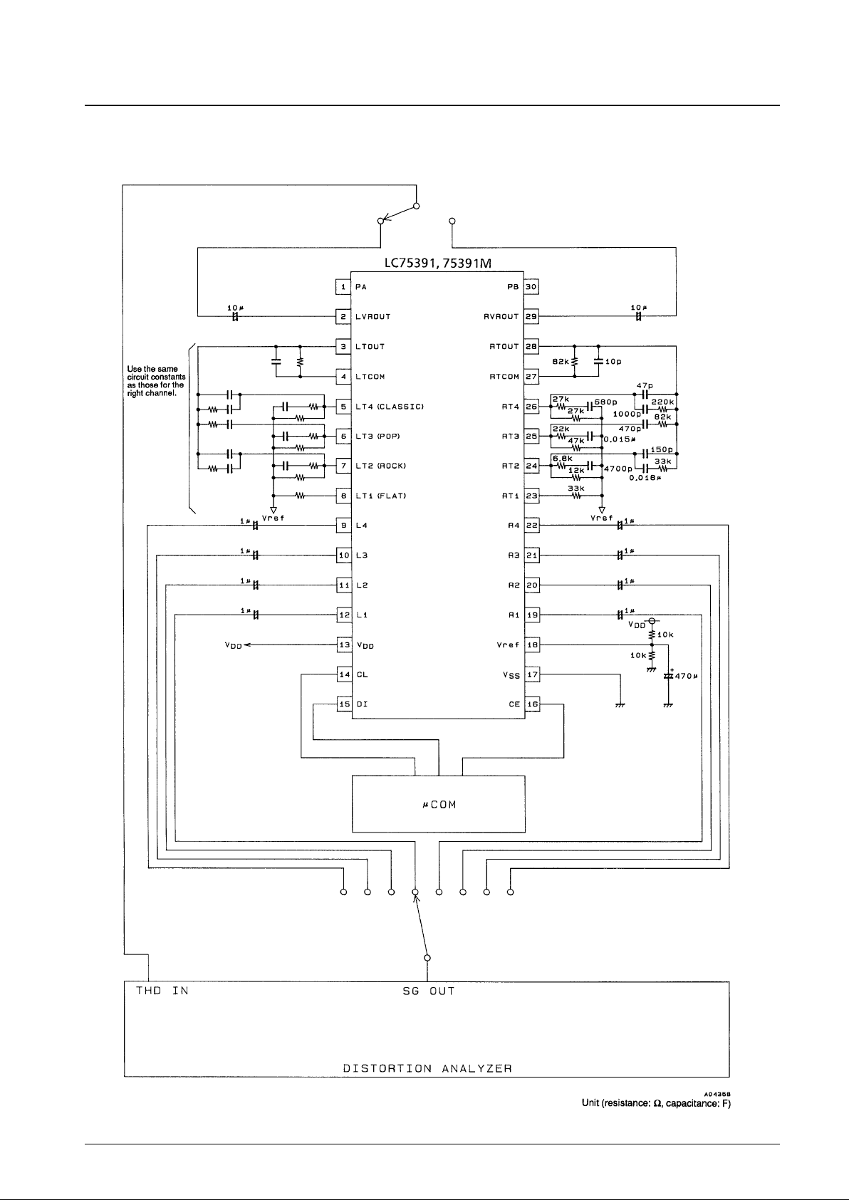
Test Circuits
1. Total harmonic distortion
No. 5201-4/13
LC75391, 75391M
Page 5

2. Output noise voltage
No. 5201-5/13
LC75391, 75391M
Page 6

3. Crosstalk
No. 5201-6/13
LC75391, 75391M
Page 7

Pin Assignment
Pin Functions
No. 5201-7/13
LC75391, 75391M
Pin No. Symbol Function
1
30
2
29
3
28
4
27
PA
PB
LVROUT
RVROUT
LTOUT
RTOUT
LTCOM
RTCOM
Digital CMOS output port
Volume control circuit outputs
Tone control circuit outputs
Tone control circuit operational amplifier inverting inputs
Continued on next page.
Circuit configuration
Page 8

Continued from preceding page.
No. 5201-8/13
LC75391, 75391M
Pin No. Symbol Function
8
7
6
5
23
24
25
26
12
11
10
9
19
20
21
22
13
18
17
14
15
16
LT1
LT2
LT3
LT4
RT1
RT2
RT3
RT4
L1
L2
L3
L4
R1
R2
R3
R4
V
DD
Vref
V
SS
CL
DI
CE
Connections for the external components that determine the tone
control pattern
Audio signal inputs and outputs
Power supply
Analog system ground
Ground
Serial data and clock inputs for device control
Chip enable
Data is read into internal latches and all analog switches change state
when this input changes from high to low.
Data transfer is enabled when this input is high.
Circuit configuration
Page 9

Volume Control Equivalent Circuit
No. 5201-9/13
LC75391, 75391M
Page 10

Control System Timing and Data Formats
The LC75391 is controlled by applying the stipulated data to the CE, CL, and DI pins. The data structure consists of a
total of 32 bits, of which 8 bits are address and 24 bits are data.
Note: The bits D20, D21, and D22 are test mode selection bits. These bits must be set to 0 by user applications.
No. 5201-10/13
LC75391, 75391M
Page 11

Application Circuit Example 1 (3-input type)
Usage Notes
1. The internal analog switch states are undefined when power is first applied. Signals should be muted externally until
the control data has been set up.
2. Cover the CL, DI, and CE pin signal lines with the ground pattern or use shielded cable for those lines to prevent the
high-frequency digital signals transmitted to the CL, DI, and CE pins from entering the analog system as noise.
3. Use bipolar capacitors if at all possible for capacitors for which no polarity is indicated.
4. We recommend making large changes in the electronic volume control setting, such as from 0 dB to –∞ dB, by using
several intermediate steps as shown in the example below. This can reduce the switching noise associated with large
changes.
Example: 0 dB → –10 dB → –20 dB → –40 dB → –70 dB → –∞
No. 5201-11/13
LC75391, 75391M
Page 12

Application Circuit Example 2 (4-input type)
Usage Notes
1. The internal analog switch states are undefined when power is first applied. Signals should be muted externally until
the control data has been set up.
2. Cover the CL, DI, and CE pin signal lines with the ground pattern or use shielded cable for those lines to prevent the
high-frequency digital signals transmitted to the CL, DI, and CE pins from entering the analog system as noise.
3. If at all possible, use bipolar capacitors for capacitors which have no polarity indicated.
4. We recommend using several intermediate steps as shown in the example below to make large changes in the
electronic volume control setting, such as from 0 dB to –∞ dB. This can reduce the switching noise associated with
these large changes.
Example: 0 dB → –10 dB → –20 dB → –40 dB → –70 dB → –∞
No. 5201-12/13
LC75391, 75391M
Page 13

PS No. 5201-13/13
LC75391, 75391M
This catalog provides information as of November, 1995. Specifications and information herein are subject to
change without notice.
■ No products described or contained herein are intended for use in surgical implants, life-support systems, aerospace
equipment, nuclear power control systems, vehicles, disaster/crime-prevention equipment and the like, the failure of
which may directly or indirectly cause injury, death or property loss.
■ Anyone purchasing any products described or contained herein for an above-mentioned use shall:
➀ Accept full responsibility and indemnify and defend SANYO ELECTRIC CO., LTD., its affiliates, subsidiaries and
distributors and all their officers and employees, jointly and severally, against any and all claims and litigation and all
damages, cost and expenses associated with such use:
➁ Not impose any responsibility for any fault or negligence which may be cited in any such claim or litigation on
SANYO ELECTRIC CO., LTD., its affiliates, subsidiaries and distributors or any of their officers and employees
jointly or severally.
■ Information (including circuit diagrams and circuit parameters) herein is for example only; it is not guaranteed for
volume production. SANYO believes information herein is accurate and reliable, but no guarantees are made or implied
regarding its use or any infringements of intellectual property rights or other rights of third parties.
 Loading...