

Page 1

CMOS LSI
Ordering number : EN5588
22798HA (OT) No. 5588-1/21
SANYO Electric Co.,Ltd. Semiconductor Bussiness Headquarters
TOKYO OFFICE Tokyo Bldg., 1-10, 1 Chome, Ueno, Taito-ku, TOKYO, 110-8534 JAPAN
Electronic Volume Control
for Car Stereo Systems
LC75373E
Overview
The LC75373E is an electronic volume control that can
implement volume, balance, fader, bass/treble + super
bass, loudness, input switching, and input/output level
control functions with a minimal number of external
components.
Functions
• Volume: Provides 81 positions, from 0 dB to –79 dB (in
1-dB steps) and –∞. A balance function can be
implemented by controlling the left and right channels
independently.
• Fader: This function can attenuate either the rear or the
front outputs over 16 positions. (From 0 to –20 dB in
2-dB steps, from –20 to –25 dB in one 5-dB step, from
–25 to –45 dB in 10-dB steps, –60 dB, and –∞.)
• Bass/treble: Forms an NF-type tone control circuit with
the addition of external capacitors. The base and treble
controls each have 15 positions.
• Input gain: The input signal can be amplified from 0 dB
to +18.75 dB in 1.25 dB steps.
• Output gain: One of two output of 0 dB and + 6.5 dB
can be selected for fader output.
• Input switch: The signal can be selected from one of
four inputs for each of the left and right channels.
• Super bass: The position of super bass can be controlled
in 11 steps.
Features
• On-chip buffer amplifiers for a minimum of external
components.
• Built-in reference voltage generation circuit
• Serial data input: Supports CCB format communication
with the system controller.
Package Dimensions
unit: mm
3148-QFP44MA
SANYO: QIP44MA
[LC75373E]
• CCB is a trademark of SANYO ELECTRIC CO., LTD.
• CCB is SANYO’s original bus format and all the bus
addresses are controlled by SANYO.
Specifications
Absolute Maximum Ratings at Ta = 25°C, VSS= 0 V
Parameter Symbol Conditions Ratings Unit
Maximum supply voltage V
DD
max V
DD
11 V
Maximum input voltage V
IN
max CL, DI, CE VSS– 0.3 to VDD+ 0.3 V
Operating temperature Topr –40 to +85 °C
Storage temperature Tstg –50 to +125 °C
Page 2
Allowable Operating Ranges at Ta = 25°C, VSS= 0 V
Electrical Characteristics at Ta = 25°C, VDD= 8 V, VSS= 0 V
Note: Values in parenthesis are targets and will be fixed after evaluation.
No. 5588-2/21
LC75373E
Parameter Symbol Conditions min typ max Unit
Supply voltage V
DD
V
DD
6.0 10.5 V
Input high-level voltage V
IH
CL, DI, CE 4.0 V
DD
V
Input low-level voltage V
IL
CL, DI, CE V
SS
1.0 V
Input voltage amplitude V
IN
CL, DI, CE, LVRIN, RVRIN, L1 to L4, R1 to R4
V
SS
V
DD
Vp-p
LFIN, RFIN, LSIN, RSIN
Input pulse width t
øW
CL 1 µs
Setup time tsetup CL, DI, CE 1 µs
Hold time thold CL, DI, CE 1 µs
Operating frequency fopg CL 500 kHz
Parameter Symbol Conditions min typ max Unit
[Input Block]
Maximum input gain Gin max +18.75 dB
Step resolution Gstep +1.25 dB
[Output Block]
Maximum output gain Gout max +6.5 dB
[Volume Control Block]
Step resolution ATstep 1 dB
Step error ATerr
step = 0 to –20 dB –1 0 +1 dB
step = –20 to –50 dB –3 0 +3 dB
[Fader Volume Block]
step =0 to –20 dB 2
Step resolution ATstep step = –20 to –25 dB 5 dB
step = –25 to –45 dB 10
Step error ATerr
step = 0 to –45 dB –2 0 +2 dB
step = –45 to –60 dB –3 0 +3 dB
Output load resistance R
L
10 kΩ
[Bass/Treble Control Block]
Bass control range Gbass Max. boost/cut ±9 ±10.5 ±12 dB
Treble control range Gtre Max. boost/cut ±8 ±10.5 ±13 dB
[Super Bass Block 1 (Type GEQ)]
Control range Crange Max. boost +17 dB
Step resolution ATstep +1.7 dB
[Super Bass Block 2 (Type T)]
Control range Crange Max. boost +20 dB
Step resolution ATstep +2.0 dB
[Overall Characteristics]
Total harmonic distortion THD V
IN
= 1 Vrms, f = 1 kHz, all settings flat overall 0.003 0.01 %
Crosstalk CT
V
IN
= 1 Vrms, f = 1 kHz, all settings flat overall,
80.5 dB
Rg = 1 kΩ
Output at maximum attenuation V
O
min VIN= 1 Vrms, f = 1 kHz, main volume at –∞ –80 dB
Output noise voltage
V
N
1 All settings flat overall (IHF-A), Rg = 1 kΩ 8 µV
V
N
2 All settings flat overall (DIN-AUDIO), Rg = 1 kΩ 10 µV
Input high-level current I
IH
CL, DI, CE: VIN= 8 V 10 µA
Input low-level current I
IL
CL, DI, CE: VIN= 0 V –10 µA
Page 3
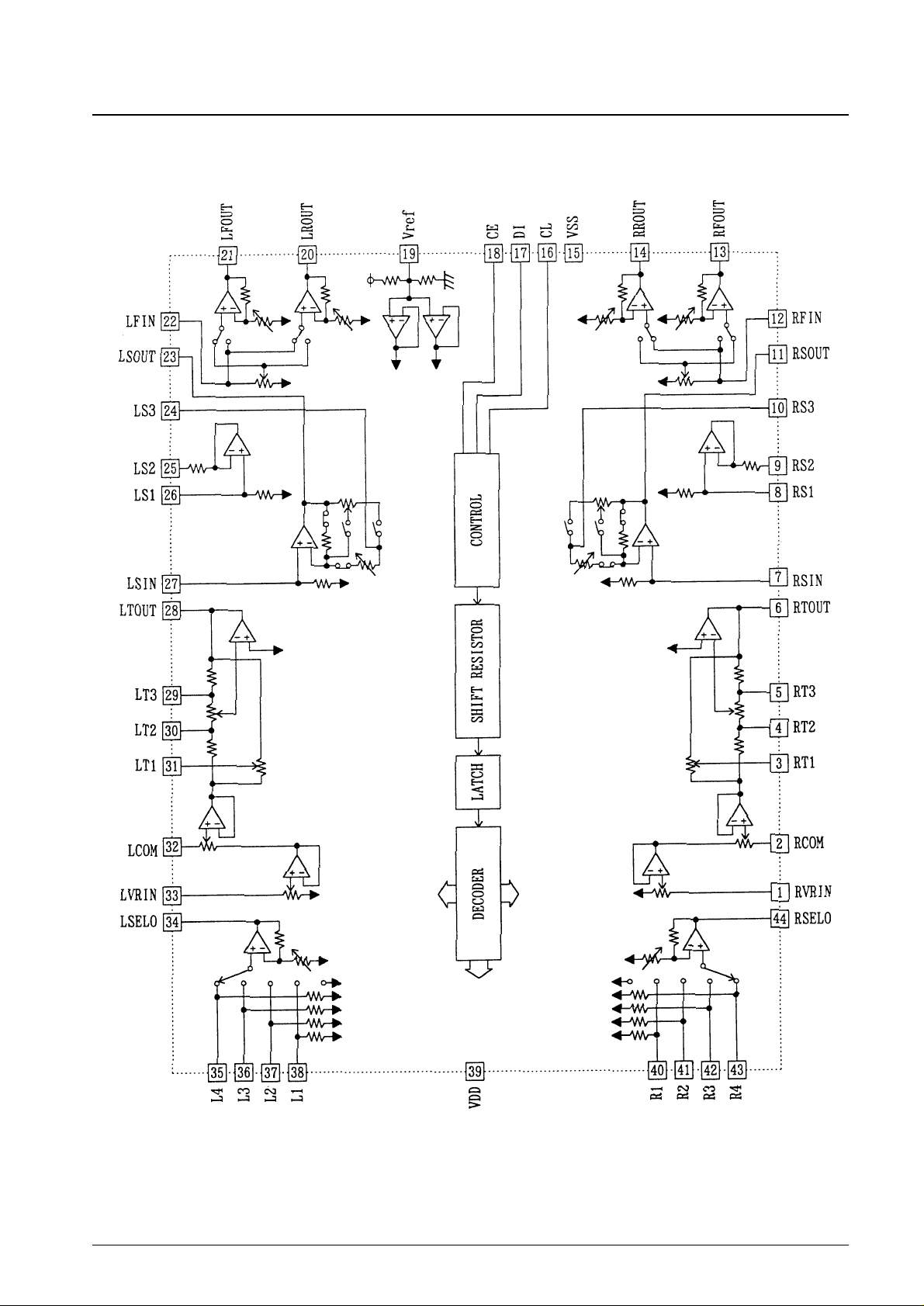
Equivalent Circuit Block Diagram
No. 5588-3/21
LC75373E
Page 4
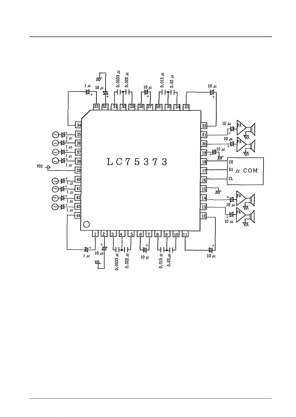
Sample Application Circuit
1. When super bass circuit 1 (Type GEQ) is used
No. 5588-4/21
LC75373E
Unit (capacitance: F)
Page 5
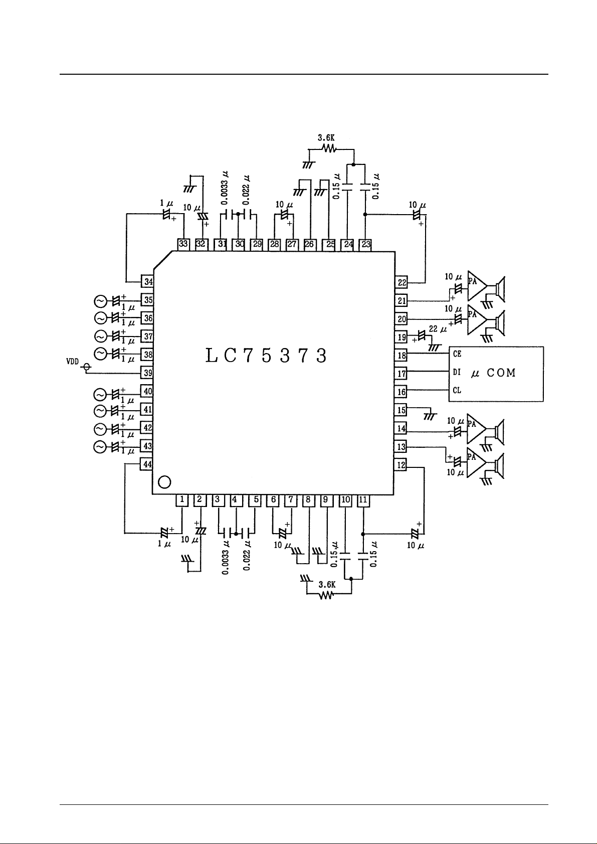
2. When super bass circuit 2 (Type T) is used
No. 5588-5/21
LC75373E
Unit (capacitance: F)
Unit (resistance: Ω)
Page 6
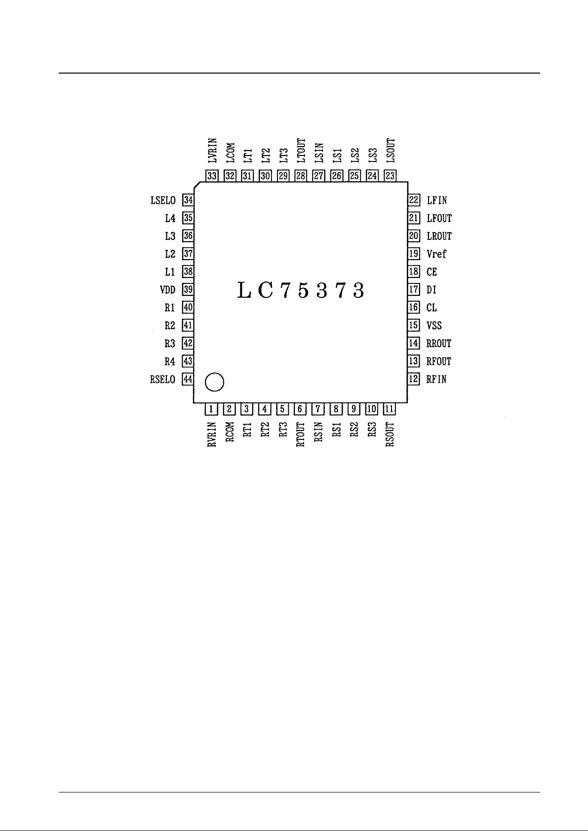
Pin Assignment
No. 5588-6/21
LC75373E
Top view
Page 7
No. 5588-7/21
LC75373E
Pin Functions
Pin No. Symbol Function Note
19
20
21
14
13
22
12
28
6
31
30
29
3
4
5
26
25
24
8
9
10
33
1
Vref
LROUT
LFOUT
RROUT
RFOUT
LFIN
RFIN
LTOUT
RTOUT
LT1
LT2
LT3
RT1
RT2
RT3
LS1
LS2
LS3
RS1
RS2
RS3
LVRIN
RVRIN
• 1/2 V
DD
voltage generation block. A capacitor must be connected between
Vref and V
SS
to suppress power supply ripple.
• Fader outputs. The front and rear systems can be attenuated independently.
• Fader inputs
• Must be driven from low-impedance circuits.
• Tone control outputs
• Connections for the bass and treble compensation capacitors for the tone
control circuit
Connect high-band compensation capacitors between T1 and T2.
Connect low-band compensation capacitors between T2 and T3.
• Super bass compensation capacitors
• 4-dB volume control inputs
• These inputs must be driven from low-impedance circuits.
Continued on next page.
Page 8

No. 5588-8/21
LC75373E
Continued from preceding page.
Pin No. Symbol Function Note
34
44
38
37
36
35
40
41
42
43
39
15
18
16
17
32
2
27
7
11
23
LSELO
RSELO
L1
L2
L3
L4
R1
R2
R3
R4
V
DD
V
SS
CE
CL
DI
LCOM
RCOM
LSIN
RSIN
RSOUT
LSOUT
• Outputs from the input selector
• Signal inputs
Power supply connection
Ground
Chip enable. Data is latched internally at the point this pin goes from high to
low. The analog switches operate at that point. Data transfer is enabled when
this pin is high.
Inputs for the serial data and clock used for LSI control.
1-dB block common outputs
• Super bass inputs
• These inputs must be driven by low-impedance circuits.
• Super bass outputs
Page 9

Input Block Equivalent Circuit
No. 5588-9/21
LC75373E
Page 10

Main Volume Control Equivalent Circuit
No. 5588-10/21
LC75373E
Page 11

Tone Control Block Equivalent Circuit
No. 5588-11/21
LC75373E
Page 12

Super Bass Block Equivalent Circuit
Note: Concerning super bass switching control
• If the Q for super bass 1 (Type GEQ) is to be set to a relatively large value
SW1.............on (Note that this switch should be set to the off position only if STEP 0 data was sent.)
SW2.............on
SW3.............off
SW4.............off
• If the Q for super bass 2 (Type T) can be set to a relatively small value without problem
SW1.............off
SW2.............off
SW3.............on
SW4.............on
No. 5588-12/21
LC75373E
Page 13

Super Bass Block Circuit 1 External Capacitor Calculation Example
The LC75373E external capacitors function as the structural elements for simulated inductances. This section presents
the equivalent circuits and the formulas used to calculate the desired center frequencies.
Simulated Inductance Equivalent Circuit
Sample Calculations
Specifications: Center frequency: F0 = 100 Hz
Q at maximum boost: Qmax = 1.05
① Determine the sharpness Q0 of the simulated inductance itself.
Q0 = * Qmax ≈ 2.6481
➁Determine C1.
C1 = ≈ 0.60 (µF)
➂ Determine C2
C2 = ≈ 0.014 (µF)
*: See the super bass block equivalent circuit diagram for the values of the internal resistors.
No. 5588-13/21
LC75373E
(RT2 + Rfeed)
RT2
1
2* π * F0 * RT2 * Q0
Q0
2* π * F0 * RT3
Page 14

Fader Volume Control Block Equivalent Circuit
No. 5588-14/21
LC75373E
Page 15

Control System Timing and Data Format
The LC75373E is controlled by applying serial data in the stipulated format to the CE, CL, and DI pins. The data
consists of 52 bits, of which 8 bits are the chip address and 44 bits are the data.
Note: 1. The bits D36 to D43 are LSI test bits and must be set to 0.
2. Concerning super bass switching
If the Q for super bass 1 is to be set to a relatively large value
If the Q for super bass 2 can be set to a relatively small value without problem
No. 5588-15/21
LC75373E
Page 16

No. 5588-16/21
LC75373E
Page 17

No. 5588-17/21
LC75373E
Page 18
No. 5588-18/21
LC75373E
Page 19

No. 5588-19/21
LC75373E
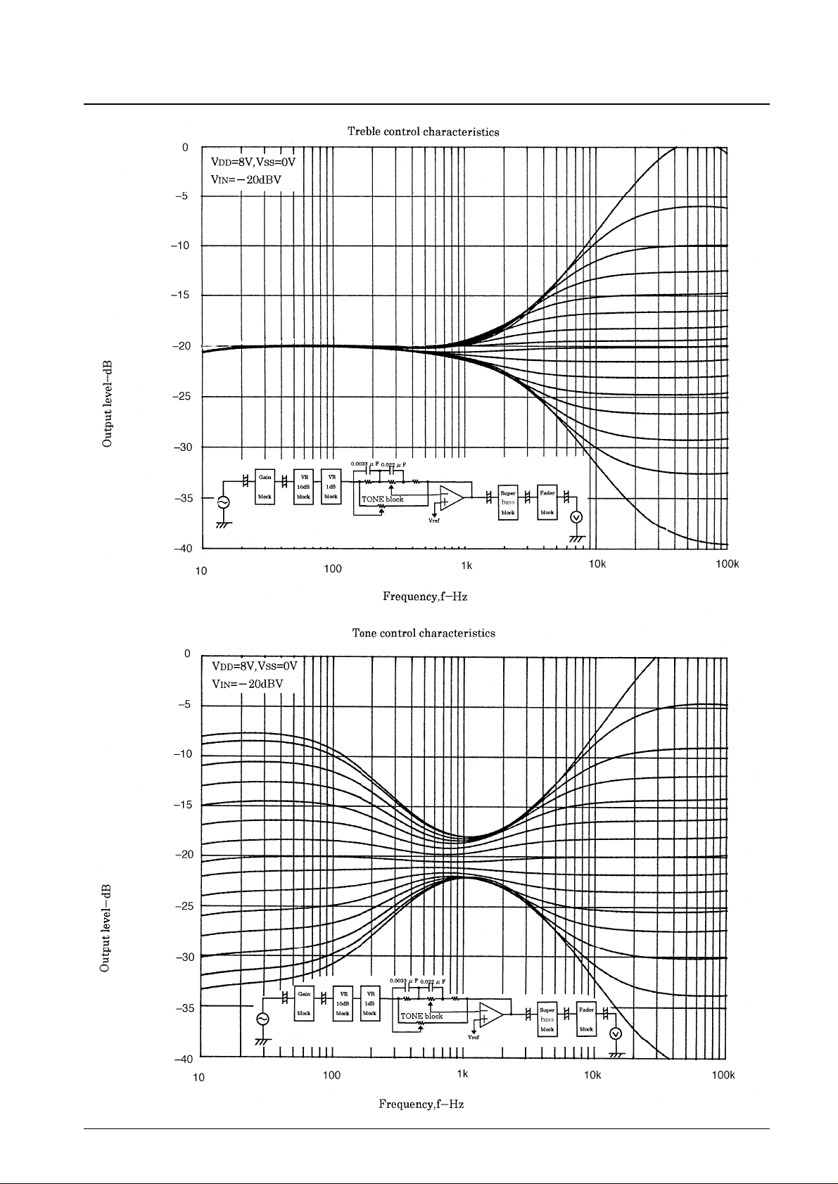
Super bass 1 Type GEQ, control characteristics
Super bass 2 Type T, control characteristics
Page 20

No. 5588-20/21
LC75373E
0.01
-30-40 -20 -10 0 10 20
30
0.1
1
Total harmonic distortion, THD-%
Outut leve, VO–dBV
f=1kHz
THD-Output level characteristics
f=20kHz
VDD=8V, VSS=0V
80-kHz low-pass weighting
overall
Gain
block
TONE
block
VR
10dB
block
VR
1dB
block
Super
bass
block
Fader
block
THD
meter
0.01
-30-40 -20 -10 0 10 20
30
0.1
1
Total harmonic distortion, THD-%
Outut leve, VIN–dBV
f=1kHz
THD-Output level characteristics
f=20kHz
VDD=8V, VSS=0V
80-kHz low-pass weighting
overall
Gain
block
TONE
block
VR
10dB
block
VR
1dB
block
Super
bass
block
Fader
block
THD
meter
THD—Input level characteristicsTHD—Output level characteristics
Total harmonic distortion, THD—%
Total harmonic distortion, THD—%
Input level, VIN—dBVOutput level, VO—dBV
Total harmonic distortion, THD—%
Page 21

PS No. 5588-21/21
LC75373E
Usage Notes
1. The states of the internal analog switches are undefined when power is first applied. Use an external muting circuit or
other technique to mute the outputs until correct control data has been set up in the LC75373E.
2. Either cover the lines connected to the CL, DI, and CE pins with the ground pattern or use shielded cable for those
lines to prevent the high-frequency digital signals on those lines from entering the analog system.
This catalog provides information as of February, 1998. Specifications and information herein are subject to
change without notice.
■ No products described or contained herein are intended for use in surgical implants, life-support systems, aerospace
equipment, nuclear power control systems, vehicles, disaster/crime-prevention equipment and the like, the failure of
which may directly or indirectly cause injury, death or property loss.
■ Anyone purchasing any products described or contained herein for an above-mentioned use shall:
➀ Accept full responsibility and indemnify and defend SANYO ELECTRIC CO., LTD., its affiliates, subsidiaries and
distributors and all their officers and employees, jointly and severally, against any and all claims and litigation and all
damages, cost and expenses associated with such use:
➁ Not impose any responsibility for any fault or negligence which may be cited in any such claim or litigation on
SANYO ELECTRIC CO., LTD., its affiliates, subsidiaries and distributors or any of their officers and employees
jointly or severally.
■ Information (including circuit diagrams and circuit parameters) herein is for example only; it is not guaranteed for
volume production. SANYO believes information herein is accurate and reliable, but no guarantees are made or implied
regarding its use or any infringements of intellectual property rights or other rights of third parties.
 Loading...