

Page 1
Ordering number : EN5330
41596HA (OT) No. 5330-1/18
Overview
The LC75372E is an electronic volume control that can
implement volume, balance, fader, bass/treble, loudness,
input switching, and input level control functions with a
minimal number of external components.
Features
• Volume: Provides 81 positions, from 0 dB to –79 dB (in
1-dB steps) and –∞. A balance function can be
implemented by controlling the left and right channels
independently.
• Fader: This function can attenuate either the rear or the
front outputs over 16 positions. (From 0 to –20 dB in
2-dB steps, from –20 to –25 dB in one 5-dB step, from
–25 to –45 dB in 10-dB steps, –60 dB, and –∞.)
• Bass/treble: Forms an NF-type tone control circuit (LUX
type) with the addition of external capacitors. The base
and treble controls each have 15 positions.
• Loudness: The volume resistor ladders are tapped
starting at the –20-dB position. A loudness function can
be implemented by adding external RC circuits at these
taps.
• The signal can be selected from one of three inputs for
each of the left and right channels. The input signals can
be amplified from 0 to +18 dB in 6-dB steps.
• On-chip buffer amplifiers for a minimum of external
components.
• Minimal switching noise due to fabrication in a silicongate CMOS process.
• Built-in reference voltage generation circuit
• Serial data input: Supports CCB format communication
with the system controller.
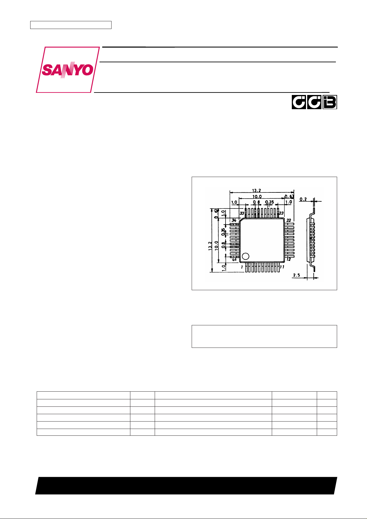
Package Dimensions
unit: mm
3148-QFP44MA
SANYO: QIP44MA
[LC75372E]
LC75372E
SANYO Electric Co.,Ltd. Semiconductor Bussiness Headquarters
TOKYO OFFICE Tokyo Bldg., 1-10, 1 Chome, Ueno, Taito-ku, TOKYO, 110-0005 JAPAN
Electronic Volume Control
for Car Stereo Systems
CMOS LSI
• CCB is a trademark of SANYO ELECTRIC CO., LTD.
• CCB is SANYO’s original bus format and all the bus
addresses are controlled by SANYO.
Specifications
Absolute Maximum Ratings at Ta = 25°C, VSS= 0 V
Parameter Symbol Conditions Ratings Unit
Maximum supply voltage V
DD
max V
DD
11 V
Maximum input voltage V
IN
max CL, DI, CE, LIN, RIN, LFIN, RFIN, L1 to L3, R1 to R3 VSS– 0.3 to VDD+ 0.3 V
Allowable power dissipation Pd max Ta ≤ 85°C 260 mW
Operating temperature Topr –40 to +85 °C
Storage temperature Tstg –50 to +125 °C
Page 2
Allowable Operating Ranges at Ta = 25°C, VSS= 0 V
Electrical Characteristics at Ta = 25°C, VDD= 9 V, VSS= 0 V
No. 5330-2/18
LC75372E
Parameter Symbol Conditions min typ max Unit
Supply voltage V
DD
V
DD
6.0 10.0 V
Input high-level voltage V
IH
CL, DI, CE 4.0 V
DD
V
Input low-level voltage V
IL
CL, DI, CE V
SS
1.0 V
Input voltage amplitude V
IN
CL, DI, CE, LIN, RIN, LFIN, RFIN, L1 to L3, R1 to R3 V
SS
V
DD
Vp-p
Input pulse width t
øW
CL 1 µs
Setup time tsetup CL, DI, CE 1 µs
Hold time thold CL, DI, CE 1 µs
Operating frequency fopg CL 500 kHz
Parameter Symbol Conditions min typ max Unit
[Input Block]
Input resistance Rin L1 to L3, R1 to R3 30 50 70 kΩ
Minimum input gain Gin min –2 0 +2 dB
Maximum input gain Gin max +16.0 +18.0 +20.0 dB
Step resolution Gstep +6.0 dB
[Volume Control Block]
Input resistance
Rv10 L10dBIN, R10dBIN: 10-dB steps, loudness off 30 50 70 kΩ
Rv1 LIN, RIN: 1-dB steps 12 20 28 kΩ
Step resolution ATstep 1 dB
Step error ATerr
step = 0 to –20 dB –1 0 +1 dB
step = –20 to –50 dB –3 0 +3 dB
[Fader Volume Block]
Input resistance Rfed LFIN, RFIN 12 20 28 kΩ
step = 0 to –20 dB 2 dB
Step resolution ATstep step = –20 to –25 dB 5 dB
step = –25 to –45 dB 10 dB
Step error ATerr
step = 0 to –45 dB –2 0 +2 dB
step = –45 to –60 dB –3 0 +3 dB
Output load resistance R
L
LFOUT, LROUT, RFOUT, RROUT 10 kΩ
[Bass/Treble Control Block]
Bass control range Gbass Max. boost/cut ±9 ±10.5 ±12 dB
Treble control range Gtre Max. boost/cut ±8 ±10.5 ±13 dB
[Overall Characteristics]
Total harmonic distortion
THD (1) V
IN
= 1 Vrms, f = 1 kHz, all settings flat overall 0.045 %
THD (2) V
IN
= 1 Vrms, f = 20 kHz, all settings flat overall 0.040 %
Crosstalk CT
V
IN
= 1 Vrms, f = 1 kHz, all settings flat overall,
80 dB
Rg = 1 kΩ
Output at maximum attenuation V
O
min
V
IN
= 1 Vrms, f = 1 kHz, main volume at –∞ –78 dB
V
IN
= 1 Vrms, f = 1 kHz, main volume at –∞, INMUTE –81 dB
Output noise voltage
V
N
(1) All settings flat overall (IHF-A), Rg = 1 kΩ 15 30 µV
V
N
(2) All settings flat overall (DIN-AUDIO), Rg = 1 kΩ 20 40 µV
Current drain I
DD
VDD– VSS= 10 V 25 30 mA
Input high-level current I
IH
CL, DI, CE: VIN= 9 V 10 µA
Input low-level current I
IL
CL, DI, CE: VIN= 0 V –10 µA
Maximum input level V
CL
All settings flat overall, measurement point; fader output
2 Vrms
THD = 1%, RL = 10 KΩ
Page 3
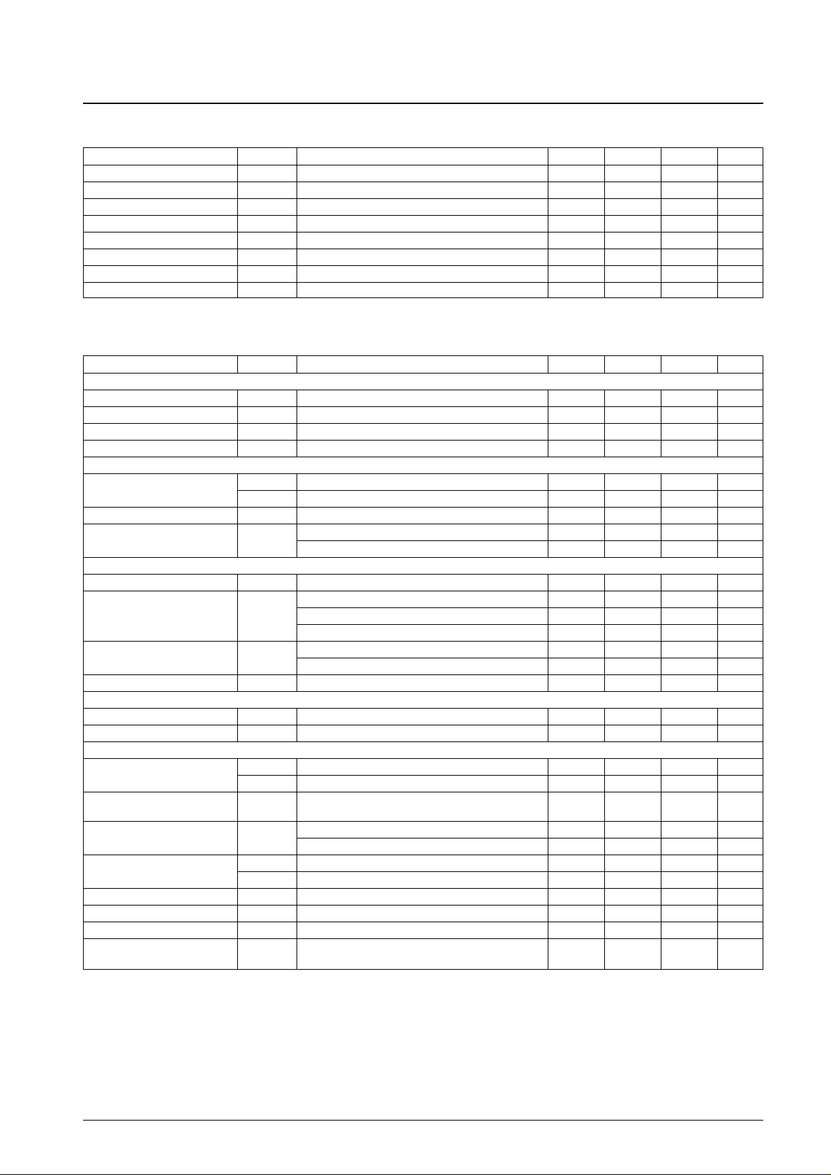
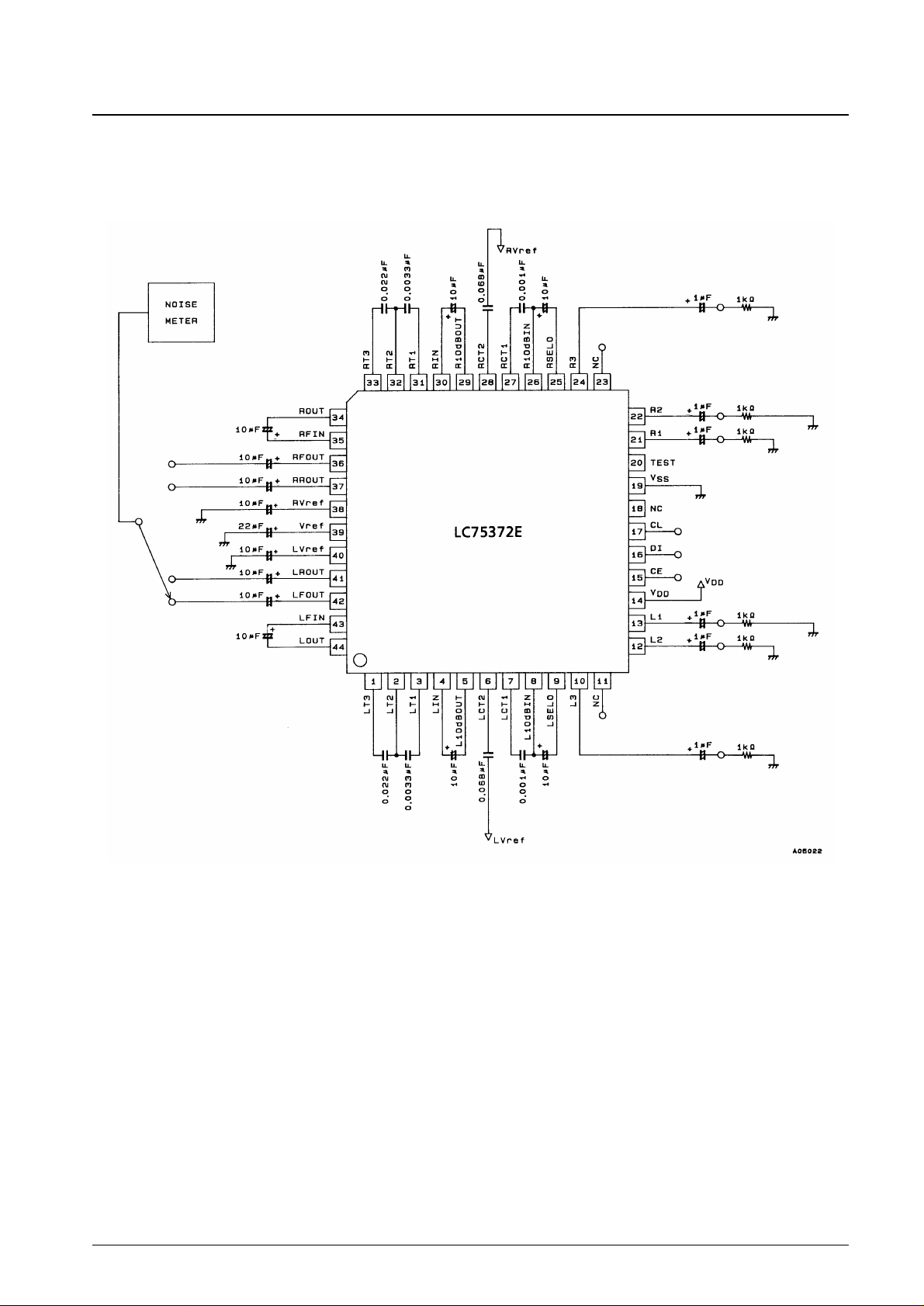
Equivalent Circuit Block Diagram and Sample Application Circuit
No. 5330-3/18
LC75372E
Page 4
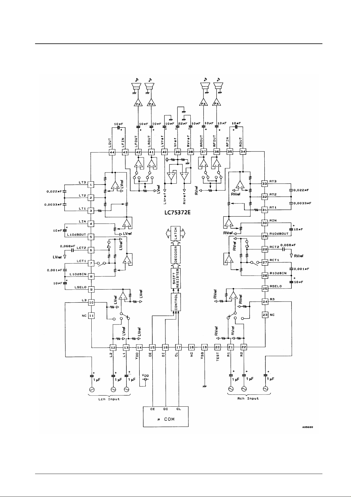
Electrical Characteristics Test Circuits
1. Total harmonic distortion
No. 5330-4/18
LC75372E
Page 5
2. Output noise voltage
No. 5330-5/18
LC75372E
Page 6
3. Crosstalk
No. 5330-6/18
LC75372E
Page 7

Pin Assignment
No. 5330-7/18
LC75372E
Page 8

Pin Functions
No. 5330-8/18
LC75372E
Pin No. Symbol Equivalent I/O circuit Function
40
38
39
41
42
37
36
43
35
44
34
3
2
1
31
32
33
7
6
27
28
LVref
RVref
Vref
LROUT
LFOUT
RROUT
RFOUT
LFIN
RFIN
LOUT
ROUT
LT1
LT2
LT3
RT1
RT2
RT3
LCT1
LCT2
RCT1
RCT2
• Common pins for the main volume block, fader volume block, tone block, gain
control block, and input switching block.
• Since the capacitors connected between LVref/RVref and V
SS
become the
residual resistance when the volume control is at maximum attenuation, the
values of these capacitors must be chosen carefully.
• The applied voltage must never exceed V
DD
.
0.488 V
DD
voltage generation block. A capacitor must be connected between
Vref and V
SS
to suppress power supply ripple.
• Fader outputs. The front and rear systems can be attenuated independently.
The amount of attenuation is the same in the left and right channels.
• Low impedance operational amplifier outputs
• Fader inputs
• Must be driven from low-impedance circuits.
Tone control outputs
Connections for the bass and treble compensation capacitors for the tone
control circuit
Connect high-band compensation capacitors between T1 and T2.
Connect low-band compensation capacitors between T2 and T3.
Loudness pins. Connect high-band compensation capacitors between
LCT1/RCT1 and L10dBIN/R10dBIN, and connect low-band compensation
capacitors between LCT2/RCT2 and LVref/RVref.
Continued on next page.
Page 9

Continued from preceding page.
No. 5330-9/18
LC75372E
Pin No. Symbol Equivalent I/O circuit Function
8
26
9
25
13
12
10
21
22
24
14
19
15
16
17
20
5
29
4
30
11
18
23
L10dBIN
R10dBIN
LSELO
RSELO
L1
L2
L3
R1
R2
R3
V
DD
V
SS
CE
DI
CL
TEST
L10dBOUT
R10dBOUT
LIN
RIN
NC
• 10-dB volume control inputs
• These inputs must be driven from low-impedance circuits.
Outputs from the input selector
Signal inputs
Power supply connection
Ground
Chip enable. Data is latched internally at the point this pin goes from high to
low. The analog switches operate at that point. Data transfer is enabled when
this pin is high.
Inputs for the serial data and clock used for LSI control.
Test input (Must be left open during normal operation.)
10-dB block outputs
• 1-dB block inputs
• These inputs must be driven by low-impedance circuits.
No-connection pins.
Page 10

Input Block Equivalent Circuit
Main Volume Control Equivalent Circuit
No. 5330-10/18
LC75372E
Page 11

Tone Control Block Equivalent Circuit
No. 5330-11/18
LC75372E
Page 12

Fader Volume Control Block Equivalent Circuit
No. 5330-12/18
LC75372E
Page 13

Sample Calculation of the Loudness Circuit External Constants
First, see the LC75372E 10-dB step internal equivalent circuit shown on page 10. Figure 1 shows a circuit to which the
loudness circuit external components have been added, and which has been simplified for this calculation. The sample
calculation below uses this circuit diagram to acquire a 5-dB boost at f = 100 Hz.
(f = 100 Hz, 5-dB boost)
Assuming that the resistors and capacitors in Figure 1 have the following values:
R1 = R2 = 50 kΩ
R3 = 5 kΩ
And C1 = Z1 and C2 = Z2.
Then:
From the above equations we find:
Z1 ≠ 891.5 kΩ and Z2 = 880 Ω.
Therefore, the specifications will be met if capacitors that have these impedances at f = 1 kHz are connected externally.
The result is that C1 = 178.5 pF and C2 = 0.18 µF.
Figure 1
R2 (R3 + Z2)
R2 + R3 + Z2
R1 · Z1
R1 + Z1
V
OUT
=
(at = 1 kHz)
= –20 dB
+
R2 (R3 + Z2)
R2 + R3 + Z2
R2 (R3 + 10 · Z2)
R2 + R3 + 10 · Z2
R1 · 10 · Z1
R1 + 10 · Z1
V
OUT
=
(at = 100 Hz)
= –15 dB
+
R2 (R3 + 10 · Z2)
R2 + R3 + 10 · Z2
No. 5330-13/18
LC75372E
Page 14

Control System Timing and Data Format
The LC75372E is controlled by applying data in the stipulated format to the CE, CL, and DI pins. The data consists of
40 bits, of which 8 bits are the chip address and 32 bits are the data.
Note: The bits D19 and D28 to D31 are LSI test bits, and must be set to 0.
No. 5330-14/18
LC75372E
Page 15

No. 5330-15/18
LC75372E
Page 16

No. 5330-16/18
LC75372E
Page 17

No. 5330-17/18
LC75372E
Page 18

PS No. 5330-18/18
LC75372E
Usage Notes
1. The states of the internal analog switches are undefined when power is first applied. Use an external muting circuit or
other technique to mute the outputs until correct control data has been set up in the LC75372E.
2. Either cover the lines connected to the CL, DI, and CE pins with the ground pattern or use shielded cable for those
lines to prevent the high-frequency digital signals on those lines from entering the analog system.
3. Muting by input switching must be used in conjunction with the volume control setting when the maximum volume
control attenuation (the VOL = –∞ position) is used.
This catalog provides information as of April, 1996. Specifications and information herein are subject to change
without notice.
■ No products described or contained herein are intended for use in surgical implants, life-support systems, aerospace
equipment, nuclear power control systems, vehicles, disaster/crime-prevention equipment and the like, the failure of
which may directly or indirectly cause injury, death or property loss.
■ Anyone purchasing any products described or contained herein for an above-mentioned use shall:
➀ Accept full responsibility and indemnify and defend SANYO ELECTRIC CO., LTD., its affiliates, subsidiaries and
distributors and all their officers and employees, jointly and severally, against any and all claims and litigation and all
damages, cost and expenses associated with such use:
➁ Not impose any responsibility for any fault or negligence which may be cited in any such claim or litigation on
SANYO ELECTRIC CO., LTD., its affiliates, subsidiaries and distributors or any of their officers and employees
jointly or severally.
■ Information (including circuit diagrams and circuit parameters) herein is for example only; it is not guaranteed for
volume production. SANYO believes information herein is accurate and reliable, but no guarantees are made or implied
regarding its use or any infringements of intellectual property rights or other rights of third parties.
 Loading...