

Page 1
Ordering number : EN6089
41399RM (OT) No. 6089-1/10
Overview
The LC7536M is an electronic volume control that
implements volume, balance, and loudness functions with
a minimum number of external components, and can be
controlled electronically with serial data.
Functions
• Volume: 81 positions from 0 to –79 dB (in 1-dB steps)
and –∞. Since the left and right channels can
be controlled separately, a balance function can
be implemented easily.
• Loudness: A tap is output from the –20 dB position of a
5 dB step volume control resistor ladder. A
loudness function can be implemented by
connecting an external RC circuit.
• S (select): Up to two LC7536M ICs can be used on the
same bus.
• Serial data input: The LC7536M supports control and
communication in the CCB format.
Features
• High voltage handling capability: ±16 V.
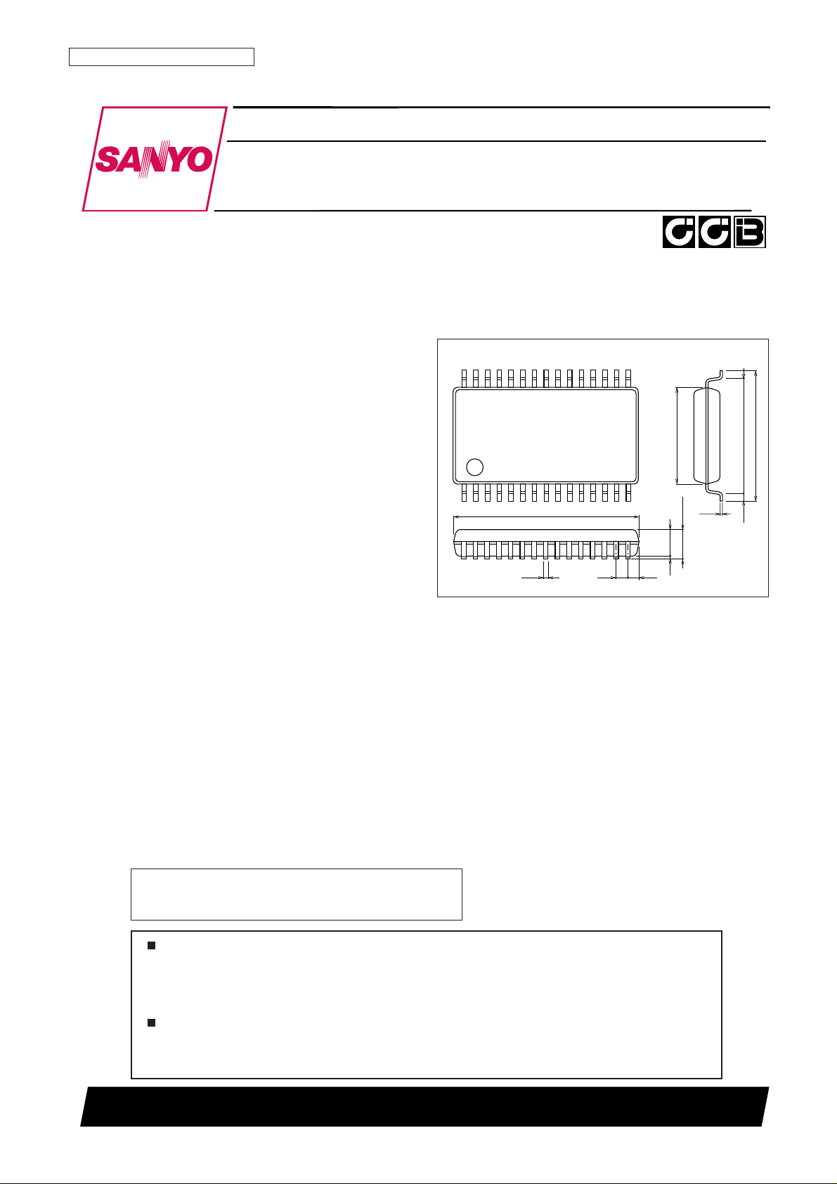
Package Dimensions
unit: mm
3216A-MFP30S
0.15
15.3
115
30 16
0.651.00.35
2.5max
2.15
0.1
0.65
7.9
9.2
10.5
SANYO: MFP30S
[LC7536M]
LC7536M
SANYO Electric Co.,Ltd. Semiconductor Company
TOKYO OFFICE Tokyo Bldg., 1-10, 1 Chome, Ueno, Taito-ku, TOKYO, 110-8534 JAPAN
Serially Controlled Electronic Volume Control that
Handles High Voltages
CMOS IC
Any and all SANYO products described or contained herein do not have specifications that can handle
applications that require extremely high levels of reliability, such as life-support systems, aircraft’s
control systems, or other applications whose failure can be reasonably expected to result in serious
physical and/or material damage. Consult with your SANYO representative nearest you before using
any SANYO products described or contained herein in such applications.
SANYO assumes no responsibility for equipment failures that result from using products at values that
exceed, even momentarily, rated values (such as maximum ratings, operating condition ranges, or other
parameters) listed in products specifications of any and all SANYO products described or contained
herein.
• CCB is a trademark of SANYO ELECTRIC CO., LTD.
• CCB is SANYO’s original bus format and all the bus
addresses are controlled by SANYO.
Page 2
No. 6089-2/10
LC7536M
Parameter Symbol Conditions Ratings Unit
V
DD
max VEE≤ VSS< VCC< V
DD
VSSto VSS+ 18 V
Maximum supply voltage V
EE
max VEE≤ VSS< VCC< V
DD
VSS– 18 to V
SS
V
V
CC
max VEE≤ VSS< VCC< V
DD
VSSto VSS+ 7 V
V
IN
max1 CL, DI, CE 0 to VCC+ 0.3 V
Maximum input voltage V
IN
max2 L5dBIN, R5dBIN, L1dBIN, R1dBIN VEE– 0.3 to VDD+ 0.3 V
V
IN
max3 S VCC– 0.3 to VDD+ 0.3 V
Allowable power dissipation Pd max Ta ≤ 75°C 250 mW
Operating temperature Topr –30 to +75 °C
Storage temperature Tstg –40 to +125 °C
Specifications
Absolute Maximum Ratings at Ta = 25°C, VSS= 0 V
Parameter Symbol Conditions
Ratings
Unit
min typ max
V
DD
V
DD
VCC+ 4.5 16 V
Supply voltage V
EEVEE
–16 0 V
V
CC
V
CC
4.5 5 5.5 V
High-level input voltage
V
IH
1 CL, DI, CE 0.8 V
CC
V
CC
V
V
IH
2 S
0.8 × (VDD– VCC) + V
CC
V
DD
V
Low-level input voltage
V
IL
1 CL, DI, CE V
SS
0.2 V
CC
V
V
IL
2 S V
CC
0.2 × (VDD– VCC) + V
CC
V
Input voltage amplitude V
IN
L5dBIN, R5dBIN, L1dBIN, R1dBIN
V
EE
V
DD
Vp-p
Input pulse width tøW CL 1 µs
Setup time t
setup
CL, DI, CE 1 µs
Hold time t
hold
CL, DI, CE 1 µs
Operating frequency fopg CL 500 kHz
Allowable Operating Ranges at Ta = –30 to +75°C, VSS= 0 V
Parameter Symbol Conditions
Ratings
Unit
min typ max
THD1
V
IN
= 1 Vrms, f = 1 kHz, all controls flat overall,
0.004 %
Total harmonic distortion
V
DD
– VEE= 32 V
THD2
V
IN
= 0.1 Vrms, f = 1 kHz, all controls flat overall,
0.02 %
V
DD
– VEE= 32 V
Crosstalk C
T
VIN= 1 Vrms, f = 1 kHz, VDD– VEE= 32 V,
–75 –60 dB
All controls flat overall, Rg = 1 kΩ
Output at maximum attenuation Vo min
VIN= 1 V rms, f = 20 kHz, volume control set at –∞,
–98 dB
V
DD
– VEE= 32 V
Output noise voltage V
N
All controls flat overall, Rg = 1 kΩ, IHF–A,
2 10 µV
V
DD
– VEE= 32 V
Total resistance
Rvol1 The 5-dB step volume block 75 kΩ
Rvol2 The 1-dB step volume block 20 kΩ
L5dBIN, R5dBIN, LCT1, RCT1, LCT2, RCT2, L5dBOUT,
Output off leakage current I
OFF
R5dBOUT, L1dBIN, R1dBIN, L1dBOUT, R1dBOUT, –10 +10 µA
LVM, RVM
High-level input current I
IH
CL, DI, CE, VIN= V
CC
+10 µA
Low-level input current I
IL
CL, DI, CE, VIN= V
SS
–10 µA
Current drain
I
DD
VDD= 16 V 1 mA
I
CC
VDD= 5.5 V 1 mA
Electrical Characteristics at Ta = 25°C, VSS= 0 V
Page 3
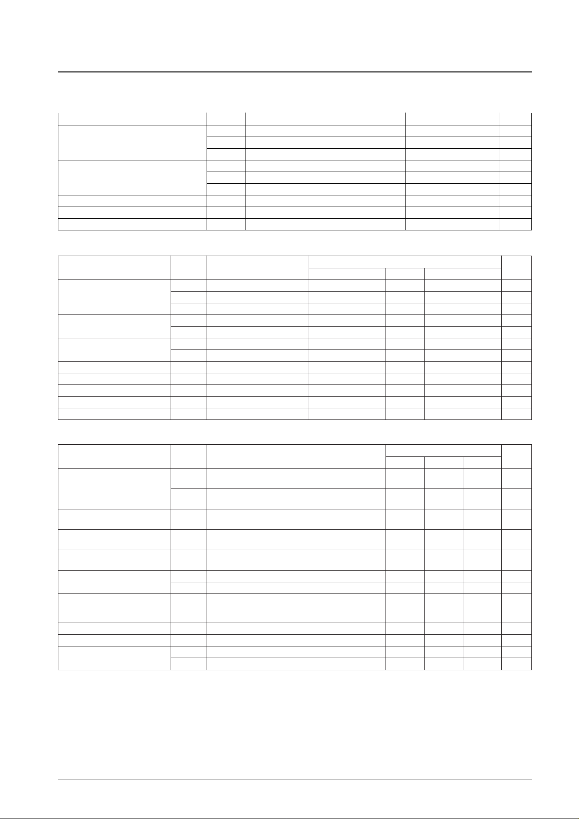
Equivalent Circuit
Sample Application Circuit
No. 6089-3/10
LC7536M
L5dBIN
LCT1
LCT2
LVM
L5dBOUT
L1dBIN
L1dBOUT
S
CE
CL
DI
R5dBIN
RCT1
RCT2
RVM
R5dBOUT
R1dBIN
R1dBOUT
V
DD
V
CC
V
SS
V
EE
LATCHL
CONTROL
LEVEL SHIFT
SHIFT REGISTER
C
D
A11989
+
+ +
+
+
L5dBIN R5dBIN
LCT1
RCT1
LCT2
RCT2
L5dBOUT
R5dBOUT
L1dBIN
R1dBIN
L1dBOUT
R1dBOUT
LVM RVM
S
CE
DI
CL
V
DD
V
CC
CE
V
CC
V
DD
DI
V
SS
CL
µ-COM
S
V
EE
V
CC
V
DD
V
EE
+–
+ –
LC7536M #1
LC7536M #2
10 µF
10 µF
1 µF
10 µF
1 µF
1 MΩ
100 kΩ
1 MΩ
0.001 µF
0.068 µF
POWER
AMP
SPEKER
A11990
Control
SPEAKER
Level shift
Latch
Shift register
Page 4

No. 6089-4/10
LC7536M
Internal Resistor Equivalent Circuit
The right channel is identical.
Test Circuit
• Total harmonic distortion
0 dB
L5dBOUT
20.570 kΩ
–5 dB
11.567 kΩ
–10 dB
6.505 kΩ
–15 dB
3.658 kΩ
–20 dB
15.868 kΩ
–25 dB
0 dB
1.407 kΩ
–1 dB
1.802 kΩ
–2 dB
1.684 kΩ
–3 dB
1.558 kΩ
–4 dB
13.548 kΩ
–∞
8.923 kΩ
5.30 kΩ
–30 dB
5.018 kΩ
–35 dB
2.822 kΩ
–40 dB
1.587 kΩ
–45 dB
0.892 kΩ
–50 dB
0.502 kΩ
–55 dB
0.282 kΩ
–60 dB
0.159 kΩ
–65 dB
0.089 kΩ
–70 dB
0.050 kΩ
–75 dB
0.065 kΩ
–∞
L1dBIN
L5dBIN L1dBOUT
LCT1
LCT2
LVM
A11991
1302293284275266257248239221021112012191318141715
16
+ +
+
+ +
10 µF
10 µF
0.001 µF
0.068 µF
1 µF
10 µF
1 µF
1 MΩ
100 kΩ
1 MΩ
V
EE
V
CC
V
DD
S.G DISTORTION ANALYZER THDin
LC7536M
A11992
The right channel is identical.
Distortion analyzer
Page 5

No. 6089-5/10
LC7536M
• Output noise voltage
Pin Assignment
1302293284275266257248239221021112012191318141715
16
+ +
+
+ +
10 µF
10 µF
0.001 µF
0.068 µF
1 µF
10 µF
1 µF
1 MΩ
1 kΩ
100 kΩ
1 MΩ
V
EE
V
CC
V
DD
Noise METER
LC7536M
A11993
• Crosstalk
+
1302293284275266257248239221021112012191318141715
16
+ +
+
+ +
10 µF
10 µF
0.001 µF
0.068 µF
1 µF
10 µF
1 µF
1 MΩ
1 kΩ
100 kΩ
1 MΩ
V
EE
V
CC
V
DD
Volt METER
S.G
+
+
+ +
10 µF
1 µF
10 µF
10 µF
1 µF
0.001 µF
0.068 µF
1 MΩ
1 MΩ
100 kΩ
LC7536M
A11994
1302293284275266257248239221021112012191318141715
16
LC7536M
A11995
NC
L5dBIN
LCT1
LCT2
L5dBOUT
NC
L1dBIN
L1dBOUT
LVM
V
EE
NC
S
V
DD
V
SS
NC NC
CL
DI
CE
NC
VCCRVM
R1dBOUT
R1dBIN
NC
R5dBOUT
RCT2
RCT1
R5dBIN
NC
(Top view)
The right channel is identical.
Noise meter
Volt meter
Page 6

No. 6089-6/10
LC7536M
Pin Functions
Pin No. Pin Function Equivalent circuit
• 5-dB step attenuator inputs
These inputs must be driven by low-impedance circuits.
2 L5dBIN
V
DD
A11996
29 R5dBIN
• Loudness circuit connections
Connect high-band compensation capacitors between the
CT1 and 5dBIN pins, and connect low-band compensation
capacitors between the CT2 and VM pins.
3 LCT1
CT2
V
DD
A11997
CT1
V
DD
A11998
28 RCT1
• 5-dB step attenuator outputs
These signals should be received by loads of about 47 kΩ
to 1 MΩ.
5 L5dBOUT
V
DD
A11999
26 R5dBOUT
• 1-dB step attenuator inputs
These inputs must be driven by low-impedance circuits.
7 L1dBIN
V
DD
A12000
24 R1dBIN
• 1-dB step attenuator outputs
These signals should be received by loads of about 47 kΩ
to 1 MΩ.
8 L1dBOUT
V
DD
A12001
• Common pins for the volume controls. The printed circuit
board pattern for these pins should be designed to have as
low an impedance as possible. Since LVM, RVM, and V
SS
are not connected internally in the IC, they may be
connected to separate external circuits that meet their
individual specifications.
Since the capacitors between the VM pins and the power
supply when a single power supply is used become the
residual resistance components at maximum attenuation,
care is required in determining the values of these
capacitors.
9 LVM
22 RVM
V
VM
5dBIN
V
DD
A12002
• Selects the address code of data during formatted.
When this pin is connected to V
DD
, the IC accepts data
when the address code is 9, and when connected to V
CC
,
it accepts data when the address code is 8.
12 S
V
DD
A12003
• Inputs for the serial data that controls the IC. The input
signals must have an amplitude of 0 to 5 V.
17 CL
18 DI
19 CE
V
DD
A12004
• Power supply connections. These pins must be connected
to the corresponding power supply. Applications must be
designed so that V
CC
is not applied before VDD.
10
V
EE
• Unused pins. These pins must be left open.
1, 6, 11,
15, 16,
20, 25,
30
NC
23 R1dBOUT
13
V
DD
14
V
SS
21
V
CC
4 LCT2
27 RCT2
Page 7

Control System Timing and Data Format
To control the LC7536M, apply the stipulated data signals to the CL, DI, and CE pins. The data consists of 20 bits, of
which 4 bits are the address and 16 bits are the data.
No. 6089-7/10
LC7536M
A1 A2 A3 D0 D1 D2 D3 D4 D5 D6 D11 D12 D13 D14 D15A0DI
CE
CL
CE
CL
DI
1 µs
min
1 µs min
1 µs
min
1 µs
min
1 µs
min
1 µs ≤ T
DST
A12005
A0 A1 A2 A3 D0 D1 D2 D3 D4 D5 D6 D7 D8 D9 D10 D11 D12 D13 D14 D15
0
1
0
0
0
1
0
0
0
0
0
0
–75 dB
D0 D1 D2 D3
–70 dB
–65 dB
1 1 0 0
–60 dB
0 0 1 0
–55 dB
1 0 1 0
–50 dB
0 1 1 0
–45 dB
1 1 1 0
–40 dB
0 0 0 1
–35 dB
1 0 0 1
–30 dB
0 1 0 1
–25 dB
1 1 0 1
–20 dB
0 0 1 1
–15 dB
1 0 1 1
–10 dB
0 1 1 1
–5 dB
1 1 1 1
0 dB
0
0
1
0
1
1
0
0
0
–∞
D4 D5 D6
–4 dB
–3 dB
0 0 1
–2 dB
1 0 1
–1 dB
0 1 1
0 dB
1000001
1
V
DD
A0 A1 A2 A3
V
CC
Don’t care
Address code
S pin
Right channel 5-dB step control
Set state
Right channel 1-dB step control
Set state
Loudness control
1: On
0: Off
Left channel 5-dB step control
(Identical to the right channel)
Don’t care
Left channel 1-dB step control
(Identical to the right channel)
Page 8

No. 6089-8/10
LC7536M
V
DD
= 16 V
V
EE
=
-
16 V
V
SS
= 0 V
VM = 0 V
V
IN
=
-
10 dBV
80 kHz L.P.F
V
DD
= 16 V
V
EE
=
-
16 V
V
SS
= 0 V
VM = 0 V
V
IN
=
-
10 dBV
80 kHz L.P.F
V
DD
= 16 V, V
EE
= -16 V
V
SS
= 0 V, VM = 0 V
V
IN
= 0 dBV
V
DD
= 16 V
V
EE
=
-
16 V
V
SS
= 0 V
VM = 0 V
V
IN
= 0 dBV
f = 1 kHz
RL = 100 kΩ
0dB
-
10dB
-
20dB
-
30dB
-100
-
∞ -70 -60 -50 -40 -30 -20 -10 0
-120
-80
-60
-40
-20
0
-25
-30
-20
-15
-10
-5
0
5
10
32 5 7 32 5 7 32 5 7 32 5 7
10 100 1k 100k10k
32 5 732 5 732 5 732 5 7
1.0
0.1
10
0.01
3
2
5
7
3
2
5
7
3
2
5
7
3
2
5
7
0.001
0.0001
100 1k 100k10k
3
2
5
7
32 5 732 5 732 5 732 5 7
1.0
10
3
2
5
7
0.1
3
2
5
7
0.01
0.001
100 1k 100k10k
LA6462
LC7536M
CT1
CT2
V
DD
+16 V
–16 V
+16 V
–16 V
V
EE
V
SS
L/RVM
LA6462
1 MΩ
1 MΩ
0.001 µF0.068 µF
+
-
+
-
LA6462
LC7536M
CT1
CT2
V
DD
+16 V
–16 V
V
EE
V
SS
L/RVM
LA6462
1 MΩ
1 MΩ
0.001 µF0.068 µF
+
-
+
-
LA6462
LC7536M
CT1
CT2
V
DD
+16 V
–16 V
V
EE
V
SS
L/RVM
LA6462
1 MΩ
1 MΩ
0.001 µF0.068 µF
+
-
+
-
LA6462
LC7536M
V
DD
V
EE
V
SS
L/RVM
1 MΩ
+
-
Volume Control Step Characteristics
Volume attenuation, — dB
Step, — dB
Loudness Characteristics
Total Harmonic Distortion — Frequency Characteristics (1)
Total Harmonic Distortion — Frequency Characteristics (2)
Output level, — dBV
Total harmonic distortion, THD — %
Total harmonic distortion, THD — %
Frequency, f — Hz
Frequency, f — Hz
Frequency, f — Hz
Level meter
The level meter input impedance
is 100 KΩ.
Level meter
Distortion meter
Distortion meter
With the volume control
at the –20 dB setting
With the volume control
at the 0 dB setting
With the volume control
at the –10 dB setting
With the volume control
at the 0 dB setting
Page 9

No. 6089-9/10
LC7536M
V
DD
= 16 V
V
EE
=
-
16 V
VM = 0 V
V
SS
= 0 V
80 kHz L.P.F
VR = 0 dB
position
V
DD
= 16 V
V
EE
=
-
16 V
VM = 0 V
V
SS
= 0 V
80 kHz L.P.F
VR =
-
20 dB position
VM = 0 V
V
SS
= 0 V
V
IN
= 0 dBV
80 kHz L.P.F
VR = 0 dB
VM = 0 V
V
SS
= 0 V
V
IN
= 0 dBV
80 kHz L.P.F
VR =
-
20 dB
3
2
5
7
3
2
5
7
3
2
5
7
3
2
5
7
3
2
5
7
3
2
5
7
3
2
5
7
3
2
5
7
201816
0.01
7
5
3
2
7
5
3
2
0.1
0.001
22 24 26 28 30 32
f=1kHz
f=20kHz
f=1kHz
f=20kHz
f=1kHz
f=1kHz
f=20kHz
f=20kHz
201816
1.0
0.1
0.01
2
3
5
7
2
3
5
7
22 24 26 28 30 32
-30 -25-50
0.0001
0.001
0.01
0.1
1.0
-45 -40 -35 -20 -15 -10 -5 0 5 10 15 20 25 30
-30 -25-50
0.001
0.01
0.1
1.0
10
-45 -40 -35 -20 -15 -10 -5 0 5 10 15 20 25 30
LA6462
LC7536M
CT1
CT2
V
DD
+16 V
–16 V
V
EE
V
SS
L/RVM
LA6462
1 MΩ
1 MΩ
0.001 µF0.068 µF
+
-
+
-
LA6462
LC7536M
CT1
CT2
V
DD
+16 V
–16 V
V
EE
V
SS
L/RVM
LA6462
1 MΩ
1 MΩ
0.001 µF0.068 µF
+
-
+
-
LA6462
LC7536M
CT1
CT2
V
DD
+16 V
–16 V
V
EE
V
SS
L/RVM
LA6462
1 MΩ
1 MΩ
0.001 µF0.068 µF
+
-
+
-
LA6462
LC7536M
CT1
CT2
V
DD
+16 V
–16 V
V
EE
V
SS
L/RVM
LA6462
1 MΩ
1 MΩ
0.001 µF0.068 µF
+
-
+
-
Total Harmonic Distortion — Supply Voltage Characteristics (1)
Total Harmonic Distortion — Supply Voltage Characteristics (2)
Total Harmonic Distortion — Input Level Characteristics (1)
Total Harmonic Distortion — Input Level Characteristics (2)
Total harmonic distortion, THD — %Total harmonic distortion, THD — %
Total harmonic distortion, THD — %Total harmonic distortion, THD — %
Supply voltage, VDD- VEE— V
Supply voltage, V
DD
- VEE— V
Input level, V
IN
— dBV
Input level, VIN— dBV
Distortion meter
Distortion meter
Distortion meter
Distortion meter
Page 10

PS No. 6089-10/10
LC7536M
Usage Notes
• The states of the internal analog switches are undefined when power is first applied. Applications should apply muting
to the analog signal system externally until control data has been transferred to the IC.
• To prevent noise from the high-frequency digital signals on the CL, DI, and CE pin lines from entering the analog
signal system, either shielded lines should be used for these lines, or they should be covered by the ground pattern.
This catalog provides information as of April, 1999. Specifications and information herein are subject to
change without notice.
Specifications of any and all SANYO products described or contained herein stipulate the performance,
characteristics, and functions of the described products in the independent state, and are not guarantees
of the performance, characteristics, and functions of the described products as mounted in the customer’s
products or equipment. To verify symptoms and states that cannot be evaluated in an independent device,
the customer should always evaluate and test devices mounted in the customer’s products or equipment.
SANYO Electric Co., Ltd. strives to supply high-quality high-reliability products. However, any and all
semiconductor products fail with some probability. It is possible that these probabilistic failures could
give rise to accidents or events that could endanger human lives, that could give rise to smoke or fire,
or that could cause damage to other property. When designing equipment, adopt safety measures so
that these kinds of accidents or events cannot occur. Such measures include but are not limited to protective
circuits and error prevention circuits for safe design, redundant design, and structural design.
In the event that any or all SANYO products (including technical data, services) described or contained
herein are controlled under any of applicable local export control laws and regulations, such products must
not be exported without obtaining the export license from the authorities concerned in accordance with the
above law.
No part of this publication may be reproduced or transmitted in any form or by any means, electronic or
mechanical, including photocopying and recording, or any information storage or retrieval system,
or otherwise, without the prior written permission of SANYO Electric Co., Ltd.
Any and all information described or contained herein are subject to change without notice due to
product/technology improvement, etc. When designing equipment, refer to the “Delivery Specification”
for the SANYO product that you intend to use.
Information (including circuit diagrams and circuit parameters) herein is for example only; it is not
guaranteed for volume production. SANYO believes information herein is accurate and reliable, but
no guarantees are made or implied regarding its use or any infringements of intellectual property rights
or other rights of third parties.
 Loading...