

Page 1

Overview
The LC7535M is an electronic volume and loudness
control IC that provides volume, balance, and loudness
functions with a minimal number of external components
and that can be controlled electronically.
Functions
• Volume: Provides 81 positions from 0 dB to –79 dB in
1-dB steps and –∞. A balance function can be
implemented by controlling the left and right volume
levels independently.
• Loudness: A loudness function can be implemented by
attaching external capacitors at the output tap provided
at the –20-dB position in the 5-dB step volume control.
• S (select) pin: Up to two LC7535M chips can be used on
the same bus.
• Serial data input: The LC7535M supports
communication with the controller in the CCB format.
Feature
• High voltage-handling capacity: ±16 V.
Package Dimensions
unit: mm
3216A-MFP30S
CMOS IC
53098RM (OT) No. 5760-1/9
SANYO: MFP30S
[LC7535M]
SANYO Electric Co.,Ltd. Semiconductor Bussiness Headquarters
TOKYO OFFICE Tokyo Bldg., 1-10, 1 Chome, Ueno, Taito-ku, TOKYO, 110-8534 JAPAN
Electronic Volume/Loudness Control with Serial Data
Control and High Voltage-Handling Capacity
LC7535M
Ordering number : EN5760
• CCB is a trademark of SANYO ELECTRIC CO., LTD.
• CCB is SANYO’s original bus format and all the bus
addresses are controlled by SANYO.
Parameter Symbol Conditions Ratings Unit
V
DD
max VEE≤ VSS< VCC< V
DD
VSSto VSS+ 18 V
Maximum supply voltage V
EE
max VEE≤ VSS< VCC< V
DD
VSS– 18 to V
SS
V
V
CC
max VEE≤ VSS< VCC< V
DD
VSSto VSS+ 7 V
V
IN
max1 CL, DI, CE 0 to VCC+ 0.3 V
Maximum input voltage V
IN
max2 L5dBIN, R5dBIN, L1dBIN, R1dBIN VEE– 0.3 to VDD+ 0.3 V
V
IN
max3 S VCC– 0.3 to VDD+ 0.3 V
Allowable power dissipation Pd max Ta ≤ 75°C 250 mW
Operating temperature Topr –30 to +75 °C
Storage temperature Tstg –40 to +125 °C
Specifications
Absolute Maximum Ratings at Ta = 25°C, VSS= 0 V
Parameter Symbol Conditions
Ratings
Unit
min typ max
V
DDVDD
VCC+ 4.5 16 V
Supply voltage V
EE
V
EE
–16 0 V
V
CCVCC
4.5 5 5.5 V
Input high-level voltage
V
IH
1 CL, DI, CE 0.8 V
CC
V
CC
V
V
IH
2 S 0.8 × (VDD– VCC) + V
CC
V
DD
V
Input low-level voltage
V
IL
1 CL, DI, CE V
SS
0.2 V
CC
V
V
IL
2S V
CC
0.2 × (VDD– VCC) + V
CC
V
Allowable Operating Ranges at Ta = 25°C, VSS= 0 V
Continued on next page.
Page 2
No. 5760-2/9
LC7535M
Continued from preceding page.
Parameter Symbol Conditions
Ratings
Unit
min typ max
Input voltage amplitude V
IN
L5dBIN, R5dBIN, L1dBIN, R1dBIN V
EE
V
DD
Vp-p
Input pulse width t
øw
CL 1 µs
Setup time t
set up
CL, DI, CE 1 µs
Hold time t
hold
CL, DI, CE 1 µs
Operating frequency t
opg
CL 500 kHz
Parameter Symbol Conditions
Ratings
Unit
min typ max
Total harmonic distortion THD
V
IN
= 1 Vrms, f = 1 kHz,
0.002 %
With all tone control settings flat, V
DD
– VEE= 30 V
V
IN
= 1 Vrms, f = 1 kHz,
Crosstalk C
T
With all tone control settings flat, RG = 1 kΩ, 70 dB
V
DD
– VEE= 30 V
Output at maximum attenuation V
Omin
VIN= 1 V rms, f = 1 kHz, with the volume set at –∞,
–95 dB
V
DD
– VEE= 30 V
Output noise voltage V
N
With all tone control settings flat, Rg = 1 kΩ
2 10 µV
IHF-A, V
DD
– VEE= 30 V
Total resistance
Rvol1 5-dB volume control block 75 kΩ
Rvol2 1-dB volume control block 20 kΩ
L5dBIN, R5dBIN, LCT1, RCT1, LCT2, RCT2, L5dBOUT,
Output off leakage current I
OFF
R5dBOUT, L1dBIN, R1dBIN, L1dBOUT, R1dBOUT, LVM, –10 +10 µA
RVM
Input high-level current I
IH
CL, DI, CE : VIN= V
CC
10 µA
Input low-level current I
IL
CL, DI, CE : VIN= V
SS
–10 µA
Current drain
I
DD
VDD= 16 V 1 mA
I
CC
VCC= 5.5 V 1 mA
Electrical Characteristics at Ta = 25°C, VSS= 0 V
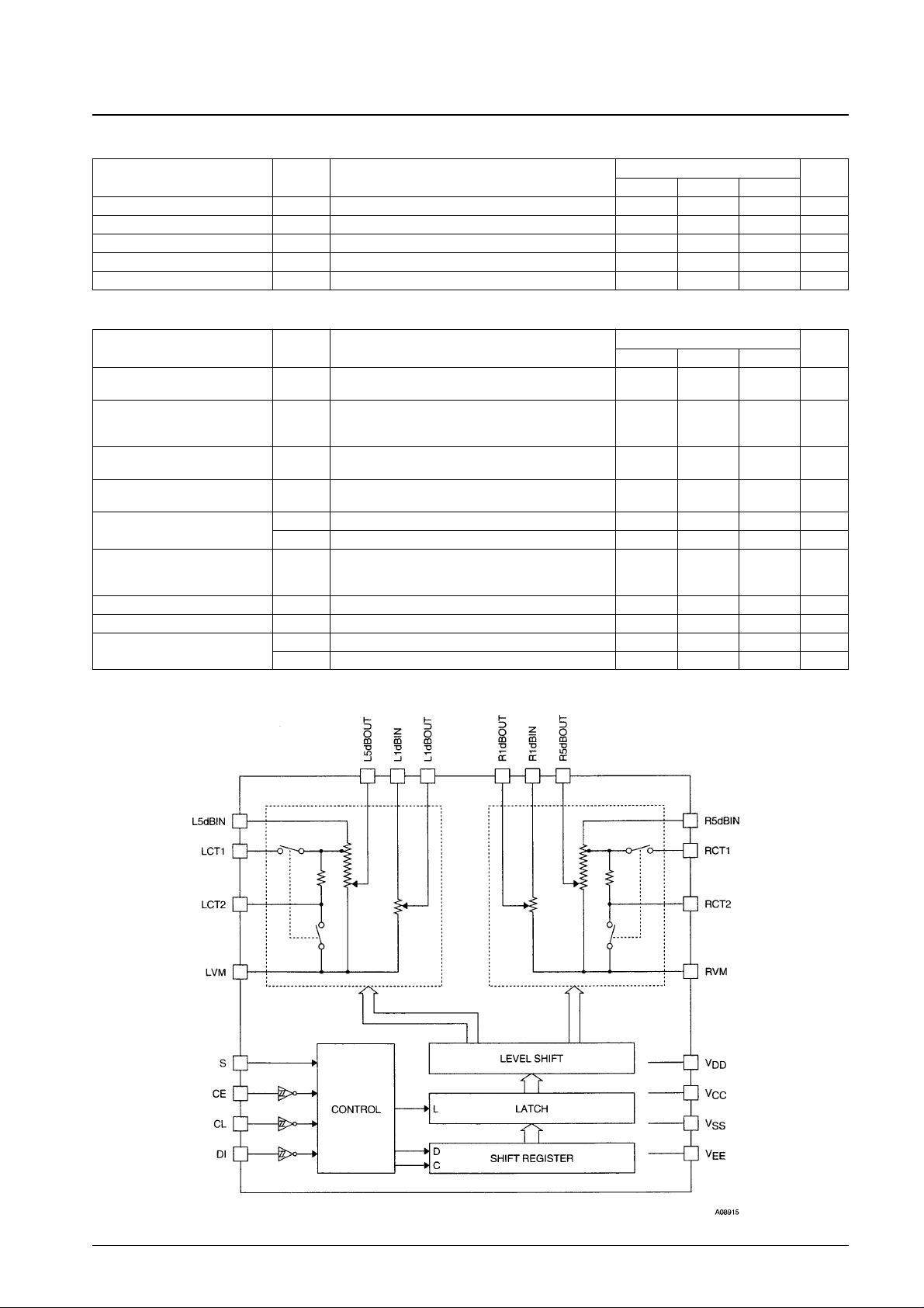
Equivalent Circuit
Page 3

Sample Application Circuit
No. 5760-3/9
LC7535M
Test Circuit
Total Harmonic Distortion
With an identical circuit for the right channel
Page 4

Output Noise Voltage
No. 5760-4/9
LC7535M
Crosstalk
Pin Assignment
With an identical circuit for the right channel
Page 5

No. 5760-5/9
LC7535M
Pin Descriptions
Pin No. Pin Function Equivalent circuit
• 5-dB step attenuator inputs
These inputs must be driven by low-impedance circuits.
2 L5dBIN
29 R5dBIN
• Loudness circuit connections
Connect the high-band compensation capacitors between the CT1 and 5dBIN pins, and
connect the low band compensation capacitors between the CT2 and the V
M
pins.
• 5-dB step attenuator outputs
These outputs must be accepted by circuits with an impedance of between 47 kΩ and 1 MΩ.
3 LCT1
28 RCT1
4 LCT2
27 RCT2
5 L5dBOUT
26 R5dBOUT
• 1-dB step attenuator inputs
These inputs must be driven by low-impedance circuits.
7 L1dBIN
24 R1dBIN
• 1-dB step attenuator outputs
These outputs must be accepted by circuits with an impedance of between 47 kΩ and 1 MΩ.
8 L1dBOUT
23 R1dBOUT
• Common connections for the volume control circuit. The impedance of the printed circuit board
pattern connected to these pins must be kept as low as possible. Since the LV
M
, RVM, and V
SS
pins are not connected internally, they must be connected externally as required by the various
specifications. When a single-sided power supply is used, the capacitors between V
M
and V
SS
become the residual resistance when the volume control is set at its maximum attenuation. This
means that care is required in selecting the values of these capacitors.
9
LV
M
• Selection input for the address code in the data format. If this pin is connected to VDD, data will
be accepted when the address code is 9, and if connected to V
CC
, data will be accepted when
the address code is 8.
12 S
22
RV
M
• Input pins for the serial data used to control the device.
These inputs must have an amplitude of 0 to 5 V. In applications in which any of microcontroller
CL, DI, or CE may go high in backup mode (when V
DD
= VCC= 0 V), the signal lines must have
series resistors of at least 2 kΩ inserted.
17 CL
• Power supply connections. All these pins must be connected to the corresponding power
supply voltage. When power is first applied, the V
CC
voltage must not rise before VDD.
10
V
EE
18 DI
19 CE
• Unconnected (NC) pins
Do not connect any signals or devices to these pins.
1, 6, 11,
15, 16,
20, 25,
30
NC
13
V
DD
14
V
SS
21
V
CC
Page 6

Control System Timing and Data Format
The stipulated serial data must be input to the CL, DI, and CE pins to control the LC7535M. The data consists of a total
of 20 bits, of which 4 bits are address and 16 bits are data.
No. 5760-6/9
LC7535M
Address code
Right channel 5-dB step control
Right channel 1-dB step control
Note *: To minimize switching
noise, applications should
input dummy data in the
following sequence: –79 dB
→ dummy → –∞
S pin
Set state
Set state
Loudness
1: On
0: Off
Left channel 5-dB step control
(identical to the right channel)
Left channel 1-dB step control
(identical to the right channel)
Dummy *
Page 7

No. 5760-7/9
LC7535M
Loudness Characteristics
VSS= VM= 0 V, loudness on
Frequency, f — Hz
Output level — dB
Overall
Step — dB
Volume attenuation — dB
Volume Step Characteristics
THD – Frequency Characteristics (1)
80-kHz low-pass weighting
80-kHz low-pass weighting
Volume control set to -20 dB
Volume control set to 0 dB
Volume control set to -10 dB
Volume control set to 0 dB
Frequency, f — Hz
Total harmonic distortion, THD — %
Frequency, f — Hz
Total harmonic distortion, THD — %
THD – Frequency Characteristics (2)
Page 8

No. 5760-8/9
LC7535M
80-kHz low-pass weighting
Flat overall
Power-supply voltage, VDD– VEE— V
Total harmonic distortion, THD — %
THD – Power-Supply Voltage Characteristics (1)
Volume control set to –20 dB
80-kHz low-pass weighting
Power-supply voltage, VDD– VEE— V
Total harmonic distortion, THD — %
THD – Power-Supply Voltage Characteristics (2)
80-kHz low-pass weighting
Flat overall
Input level, VIN– dBV
Total harmonic distortion, THD — %
THD – Input Level Characteristics (1)
80-kHz low-pass weighting
Volume control set to –20 dB
Input level, VIN– dBV
Total harmonic distortion, THD — %
THD – Input Level Characteristics (2)
Page 9

PS No. 5760-9/9
LC7535M
This catalog provides information as of May, 1998. Specifications and information herein are subject to change
without notice.
■ No products described or contained herein are intended for use in surgical implants, life-support systems, aerospace
equipment, nuclear power control systems, vehicles, disaster/crime-prevention equipment and the like, the failure of
which may directly or indirectly cause injury, death or property loss.
■ Anyone purchasing any products described or contained herein for an above-mentioned use shall:
➀ Accept full responsibility and indemnify and defend SANYO ELECTRIC CO., LTD., its affiliates, subsidiaries and
distributors and all their officers and employees, jointly and severally, against any and all claims and litigation and all
damages, cost and expenses associated with such use:
➁ Not impose any responsibility for any fault or negligence which may be cited in any such claim or litigation on
SANYO ELECTRIC CO., LTD., its affiliates, subsidiaries and distributors or any of their officers and employees
jointly or severally.
■ Information (including circuit diagrams and circuit parameters) herein is for example only; it is not guaranteed for
volume production. SANYO believes information herein is accurate and reliable, but no guarantees are made or implied
regarding its use or any infringements of intellectual property rights or other rights of third parties.
Usage Notes
• The state of the internal analog switches are undefined when power is first applied. Applications should apply external
muting to the output signal until the control data has been set up.
• To prevent the high-frequency digital signals transmitted over the CL, DI, and CE pin lines from entering the analog
signal system, these lines should either be covered by the ground pattern or shielded cables should be used.
80-kHz low-pass weighting
Flat overall
Output level, VO– dBV
Total harmonic distortion, THD — %
THD – Output Level Characteristics (1)
80-kHz low-pass weighting
Volume control set to –20 dB
Output level, VO– dBV
Total harmonic distortion, THD — %
THD – Output Level Characteristics (2)
 Loading...