

Page 1
Ordering number : ENN6867
20901RM (OT) No. 6867-1/28
Overview
The LC75343M is an electronic volume system that can
control the volume, balance, 2-band equalizer, super bass,
and input switching functions by serial data input.
Functions
• Volume: 0 dB to –78 dB (1-dB step) and –∞ (64
positions)
0 dB to –50 dB (1-dB step), –50 dB to –70 dB
(2-dB step), –70-dB to –78 dB (4-dB step)
Balance function with separate L/R control
• Treble: ±10-dB control in 2-dB steps is possible.
Shelving characteristic.
• Bass*: ±10-dB control in 2-dB steps is possible. Peaking
characteristics.
• Super bass*: +10-dB control in 2-dB steps is possible.
Peaking characteristics.
(+/–10 dB control in 2-dB steps is possible
depending on software support and the
application. Peaking characteristics.)
• Selector: 5 input signals can be selected both for
L and R
• Input gain: 0 dB to +30 dB (2-dB step) amplification is
possible for the input signal.
• General-purpose amp (ATT): 2 on-chip general-purpose
amplifiers
(0-dB to –18-dB in 2-dB
steps and –∞ 11 positions
attenuate control is
possible, depending on
software support and the
application)
Note*: Regarding (Bass) and (Super bass) above, MID
and BASS functions can also be realized by
changing the capacitor capacitance.
Features
• On-chip buffer amplifier cuts down number of external
components
• Low switching noise generated by on-chip switch due to
use of silicon gate CMOS process
• On-chip reference voltage circuit for analog ground
• Controls performed with serial data input (CCB)
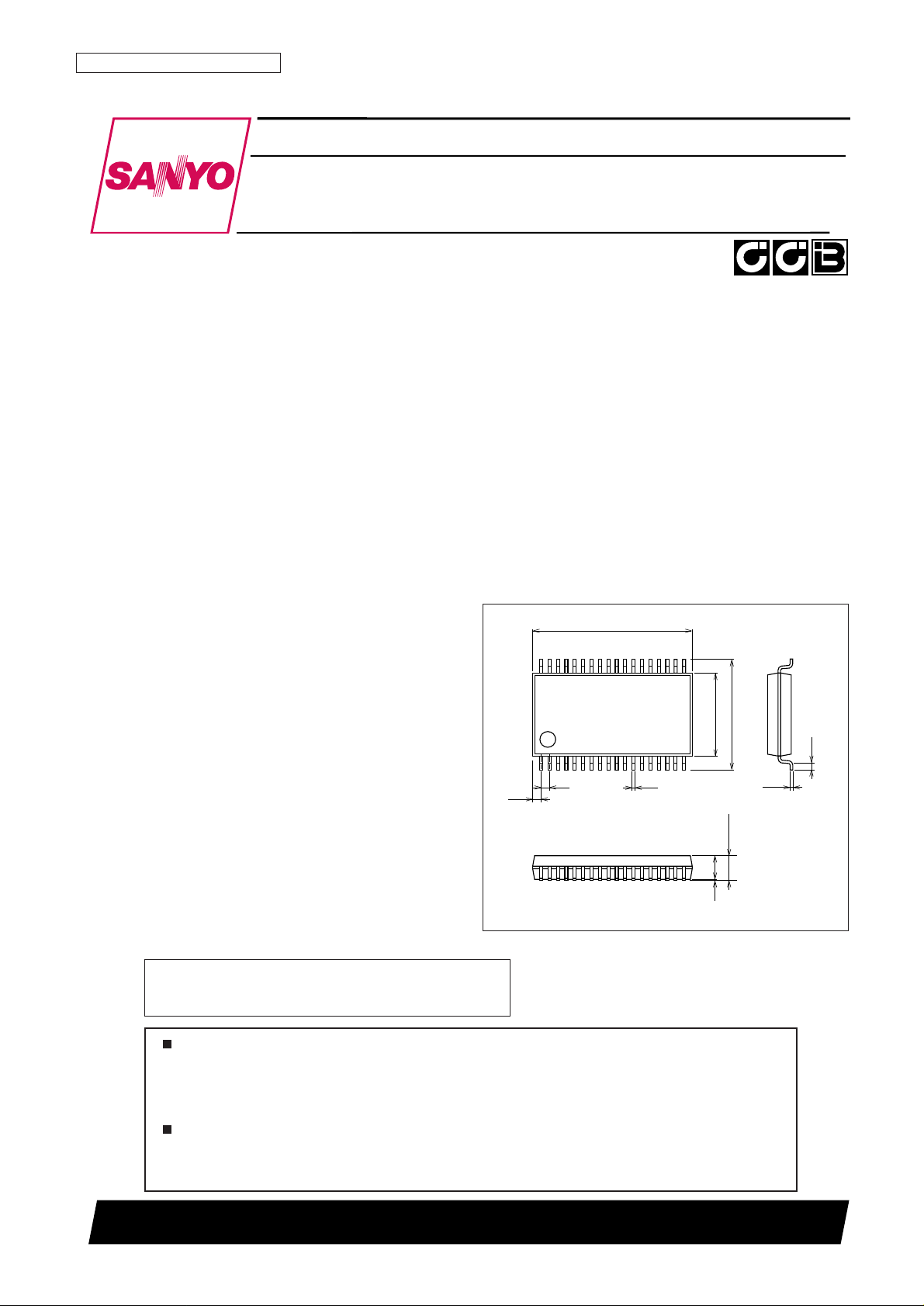
Package Dimensions
unit: mm
3263-MFP36SDJ (375 mil)
1
18
36 19
0.8
15.2
0.3
0.65
10.5
7.9
0.25
(0.8)
2.45max
0.1
(2.25)
SANYO: MFP36SDJ (375 mil)
[LC75343M]
LC75343M
SANYO Electric Co.,Ltd. Semiconductor Company
TOKYO OFFICE Tokyo Bldg., 1-10, 1 Chome, Ueno, Taito-ku, TOKYO, 110-8534 JAPAN
Electronic Volume Control System on-Chip
CMOS IC
Any and all SANYO products described or contained herein do not have specifications that can handle
applications that require extremely high levels of reliability, such as life-support systems, aircraft’s
control systems, or other applications whose failure can be reasonably expected to result in serious
physical and/or material damage. Consult with your SANYO representative nearest you before using
any SANYO products described or contained herein in such applications.
SANYO assumes no responsibility for equipment failures that result from using products at values that
exceed, even momentarily, rated values (such as maximum ratings, operating condition ranges, or other
parameters) listed in products specifications of any and all SANYO products described or contained
herein.
• CCB is a trademark of SANYO ELECTRIC CO., LTD.
• CCB is SANYO’s original bus format and all the bus
addresses are controlled by SANYO.
Page 2
Pin Assignment
No. 6867-2/28
LC75343M
LC75343M
1
2
3
4
5
6
7
8
9
10
11
12
13
14
15
16
17
18
36
35
34
33
32
31
30
29
28
27
26
25
24
23
22
21
20
19
DI
CE
VSS
LOPOUT
LINM
LINP
LOUT
LSB
LBASS2
LBASS1
LTRE
LVRIN
LSEL0
L5
L4
L3
L2
L1
CL
VDD
ROPOUT
RINM
RINP
ROUT
RSB
RBASS2
RBASS1
RTRE
RVRIN
RSEL0
R5
R4
R3
R2
R1
Vref
Page 3
No. 6867-3/28
LC75343M
Sample Application Circuit
• General-Purpose Op-Amp Specifications)
654 213635
µCOM
34 33 323
2.2 µF
2.2 µF
PA
PA
7
8
9
10
11
12
13
14 15 16 17 18 19 21 22 23 24
25
26
27
28
29
30
31
20
7.6 kΩ
CCB
interface
Control
circuit
L5
1 µFL41 µF
L3
1 µFL21 µFL11 µF
Vref
RVref
LVref
LINP
RINP
LINM
RINM
LOPOUT
ROPOUT
VSS
CE
DI
CL
VDD
22 µF
R1
1 µFR21 µFR31 µFR41 µF
R5
1 µF
Control
circuit
Logic
circuit
f0 = 100 Hz
0.1 µF
0.1 µF
0.1 µF
0.1 µF
0.1 µF
0.1 µF
LOUT
LSB
7.6 kΩ
f0 = 100 Hz
7.6 kΩ
f0 = 100 Hz
7.6 kΩ
f0 = 100 Hz
2700 pF
1 µF
2700 pF
0.1 µF
0.1 µF
1 µF
LBASS2
LBASS1
LTRE
LVRIN
LSEL0
ROUT
RSB
RTRE
RVRIN
RSEL0
RBASS2
RBASS1
Page 4
No. 6867-4/28
LC75343M
• ATT Control Specifications
654 213635
µCOM
34 33 323
2.2 µF
1 µF
1 µF
2.2 µF
7
8
9
10
11
12
13
14 15 16 17 18 19 21 22 23 24
25
26
27
28
29
30
31
20
7.6 kΩ
CCB
interface
Control
circuit
L5
1 µFL41 µF
L3
1 µFL21 µFL11 µF
Vref
RVref
LVref
LINP
RINP
LINM
RINM
LOPOUT
ROPOUT
VSS
CE
DI
CL
VDD
22 µF
R1
1 µFR21 µFR31 µFR41 µF
R5
1 µF
Control
circuit
Logic
circuit
f0 = 100 Hz
0.1 µF
0.1 µF
LOUT
LSB
7.6 kΩ
f0 = 100 Hz
7.6 kΩ
f0 = 100 Hz
7.6 kΩ
f0 = 100 Hz
2700 pF
1 µF
2700 pF
0.1 µF
0.1 µF
1 µF
LBASS2
LBASS1
LTRE
LVRIN
LSEL0
ROUT
RSB
RTRE
RVRIN
RSEL0
RBASS2
RBASS1
PA
PA
0.1 µF
0.1 µF
0.1 µF
0.1 µF
Page 5
No. 6867-5/28
LC75343M
• 3-Band Specifications
654 213635
µCOM
34 33 323
2.2 µF
2.2 µF
7
8
9
10
11
12
13
14 15 16 17 18 19 21 22 23 24
25
26
27
28
29
30
31
20
7.6 kΩ
*Bass function specs
CCB
interface
Control
circuit
L5
1 µF
L4
1 µF
L3
1 µFL21 µFL11 µF
Vref
RVref
LVref
LINP
RINP
LINM
RINM
LOPOUT
ROPOUT
VSS
CE
DI
CL
VDD
22 µF
R1
1 µFR21 µFR31 µFR41 µF
R5
1 µF
Control
circuit
Logic
circuit
f0 = 100 Hz
0.1 µF
0.1 µF
LOUT
LSB
7.6 kΩ
f0 = 1 kHz
7.6 kΩ
f0 = 100 Hz
7.6 kΩ
f0 = 1 kHz
2700 pF
1 µF
2700 pF
0.01 µF
0.01 µF
1 µF
LBASS2
LBASS1
LTRE
LVRIN
LSEL0
ROUT
RSB
RTRE
RVRIN
RSEL0
RBASS2
RBASS1
PA
PA
0.1 µF
0.1 µF
0.01 µF
0.01 µF
*MID function specs
*Bass function specs
*MID function specs
Page 6
No. 6867-6/28
LC75343M
Parameter Symbol Pin Name Conditions Ratings Unit
Maximum supply voltage V
DD
max V
DD
10.5 V
CE, DI, CL –0.3 to +10.5
Maximum input voltage VINmax
L1 to L5, R1 to R5,
V
LVRIN, RVRIN, LINP, V
SS
– 0.3 to VDD+ 0.3
RINP, LINM, RINM
Allowable power dissipation Pdmax
Ta ≤ 75°C, independent IC
520 mW
Operating temperature Topr –30 to +75 °C
Storage temperature Tstg –40 to +125 °C
Specifications
Absolute Maximum Ratings at Ta = 25°C, VSS= 0 V
Parameter Symbol Pin Name Conditions
Ratings
Unit
min typ max
Supply voltage V
DDVDD
4.5 9 V
Input high-level voltage V
IH
CL, DI, CE 2.0 9 V
Input low-level voltage V
IL
CL, DI, CE
7.5 ≤ V
DD
≤ 9VSS0.8
V
4.5 ≤ V
DD
≤ 7.5 V
SS
0.3
L1 to L5, R1 to R5,
Input amplitude voltage V
IN
LVRIN, RVRIN, LINP, V
SS
V
DD
Vp-p
RINP, LINM, RINM
Input pulse width tøW CL 1 µs
Setup time tsetup CL, DI, CE 1 µs
Hold time thold CL, DI, CE 1 µs
Operating frequency fopg CL 500 kHz
Allowable Operating Ranges at Ta = –30 to +75°C, VSS= 0 V
Parameter Symbol Pin Name Conditions
Ratings
Unit
min typ max
Maximum input gain Ginmax +30 dB
Step resolution Gstep +2 dB
Input resistance Rin
L1, L2, L3, L4, L5
50 kΩ
R1, R2, R3, R4, R5
Clipping level Vcl LSEL0, RSEL0 THD = 1.0%, f = 1 kHz 2.50 Vrms
Output load resistance Rl LSEL0, RSEL0 10 kΩ
Electrical Characteristics at Ta = 25°C, VDD= 8 V, VSS= 0 V
Input block
Parameter Symbol Pin Name Conditions
Ratings
Unit
min typ max
Input resistance Rin LVRIN, RVRIN 50 kΩ
Volume block
Parameter Symbol Pin Name Conditions
Ratings
Unit
min typ max
Control range Geq max. boost/cut ±8 ±10 ±12 dB
Step resolution Estep 1 2 3 dB
Internal feedback resistance Rfeed 51.7 kΩ
Treble band equalizer control block
Page 7
No. 6867-7/28
LC75343M
Parameter Symbol Pin Name Conditions
Ratings
Unit
min typ max
Control range Geq max. boost/cut ±8 ±10 ±12 dB
Step resolution Estep 1 2 3 dB
Internal feedback resistance Rfeed 33.1 kΩ
Bass (mid) band equalizer control block
Parameter Symbol Pin Name Conditions
Ratings
Unit
min typ max
Control range (super bass specs)
Geq
max. boost +8 +10 +12 dB
Control range (3-band specs) max. boost/cut ±8 ±10 ±12 dB
Step resolution Estep 1 2 3 dB
Internal feedback resistance Rfeed 33.1 kΩ
Super bass (bass) band equalizer control block
Parameter Symbol Conditions
Ratings
Unit
min typ max
Total harmonic distortion
0.006 0.01 %
(General-purpose op-amp specs)
THD V
IN
= 1 Vrms, f = 1 KHz, total flat overall
Total harmonic distortion
0.007 0.01 %
(ATT, 3-band specs)
Crosstalk
80 dB
(General-purpose op-amp specs)
CT V
IN
= 1 Vrms, f = 1 KHz, Rg = 1 kΩ, total flat overall
Crosstalk
80 dB
(ATT, 3-band specs)
Output noise voltage
9.3 µV
(General-purpose op-amp specs)
VN Flat overall, 80 kHz L.P.F
Output noise voltage
10.4 µV
(ATT, 3-band specs)
Maximum attenuated output
–90 dB
(General-purpose op-amp specs)
Vomin Flat overall, f = 1 kHz
Maximum attenuated characteristics
–90 dB
(ATT, 3-band specs)
Curent drain I
DD
VDD– VSS= +9 V 40 mA
Input high-level current I
IH
CL, DI, CE: VIN= 9 V 10 µA
Input low-level current I
IL
CL, DI, CE: VIN= 0 V –10 µA
General
Parameter Symbol Pin Name Conditions
Ratings
Unit
min typ max
Input resistance Rin LINP, RINP 50 kΩ
General-purpose/ATT op-amp block
Page 8
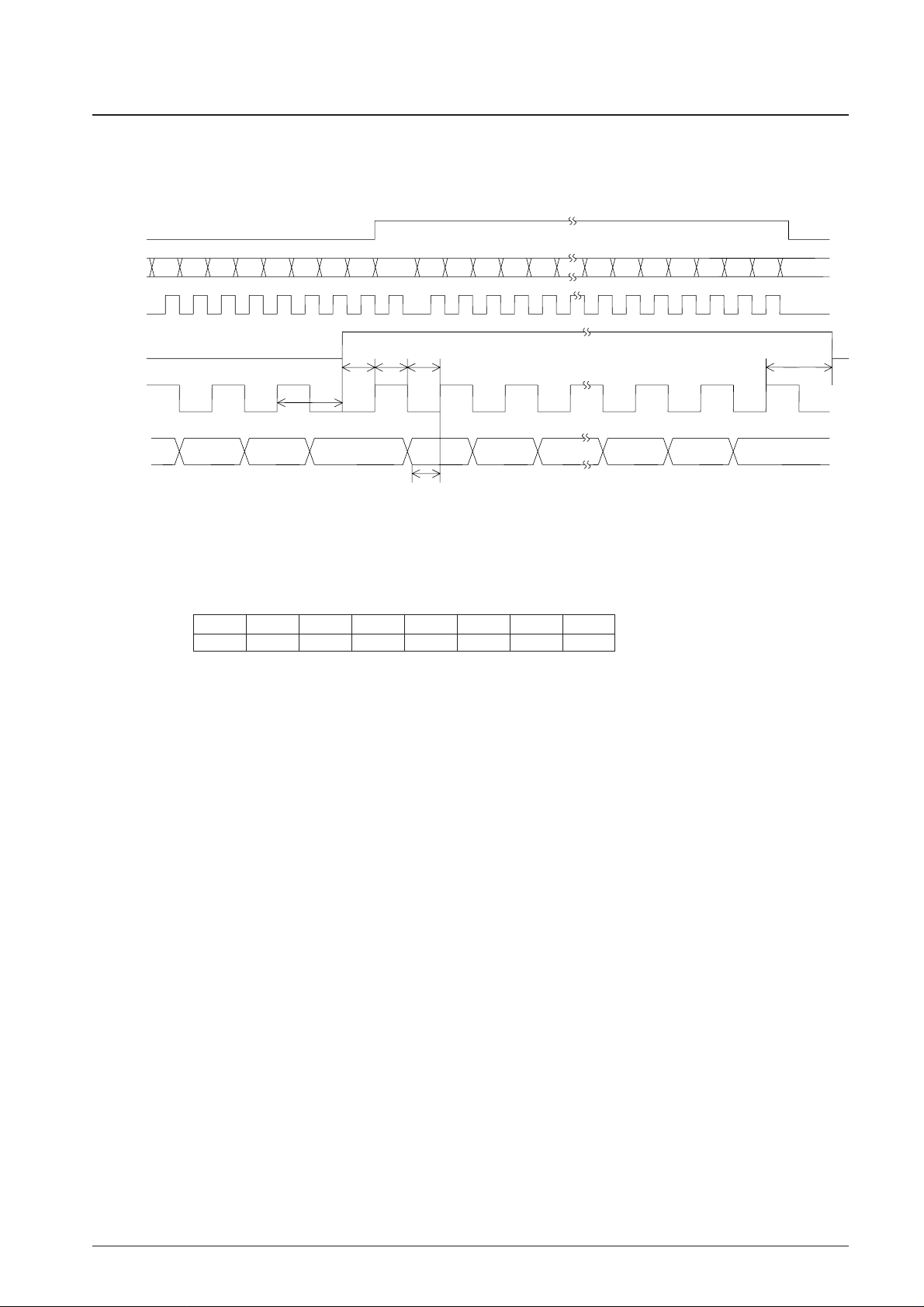
Control Timing and Data Format
To control the LC75343M, input specified serial data to the CL, DI, and CE pins. The data configuration consists of a
total of 40 bits broken down into 8 address bits and 32 data bits.
No. 6867-8/28
LC75343M
CE
B0 B1 B2 B3 A0 A1 A2 A3
1 µs
min
1 µs
min
1 µs
min
1 µs ≤ T
DEST
1 µs
min
1 µs
min
D0 D1 D2 D3 D4 D5
D25 D26 D27 D28 D29 D30 D31
DI
DI
CL
CL
CE
Address Code (B0 to A3)
The LC75343M has an 8-bit address code and common specifications with a SANYO serial bus CCB IC are
possible.
Address code
(LSB)
(82HEX)
B0 B1 B2 B3 A0 A1 A2 A3
01000001
Page 9
Control Code Allocation
General-purpose op-amp, ATT control specifications (D3 = 0)
Input switching control
(L1, L2, L3, L4, L5, R1, R2, R3, R4, R5)
No. 6867-9/28
LC75343M
D0 D1 D2 D3 Operation
0 0 0 0 L1 (R1) on
1 0 0 0 L2 (R2) on
0 1 0 0 L3 (R3) on
1 1 0 0 L4 (R4) on
0 0 1 0 L5 (R5) on
1 0 1 0 Analog ground connection
0110
Test mode
1110
Must not be used in normal operation.
3-band specifications (D3 = 1)
Input switching control
(L1, L2, L3, L4, L5, R1, R2, R3, R4, R5)
D0 D1 D2 D3 Operation
0 0 0 0 L1 (R1) on
1 0 0 0 L2 (R2) on
0 1 0 0 L3 (R3) on
1 1 0 0 L4 (R4) on
0 0 1 0 L5 (R5) on
1 0 1 0 Analog ground connection
0110
Test mode
1110
Must not be used in normal operation.
Input gain control
D4 D5 D6 D7 Operation
0000 0 dB
1 0 0 0 +2 dB
0 1 0 0 +4 dB
1 1 0 0 +6 dB
0 0 1 0 +8 dB
1 0 1 0 +10 dB
0 1 1 0 +12 dB
1 1 1 0 +14 dB
0 0 0 1 +16 dB
1 0 0 1 +18 dB
0 1 0 1 +20 dB
1 1 0 1 +22 dB
0 0 1 1 +24 dB
1 0 1 1 +26 dB
0 1 1 1 +28 dB
1 1 1 1 +30 dB
Page 10

No. 6867-10/28
LC75343M
Volume control
D8 D9 D10 D11 D12 D13 Operation
000000 0 dB
100000 –1 dB
010000 –2 dB
110001 –3 dB
001000 –4 dB
101000 –5 dB
011000 –6 dB
111000 –7 dB
000100 –8 dB
100100 –9 dB
0 1 0 1 0 0 –10 dB
1 1 0 1 0 0 –11 dB
0 0 1 1 0 0 –12 dB
1 0 1 1 0 0 –13 dB
0 1 1 1 0 0 –14 dB
1 1 1 1 0 0 –15 dB
0 0 0 0 1 0 –16 dB
1 0 0 0 1 0 –17 dB
0 1 0 0 1 0 –18 dB
1 1 0 0 1 0 –19 dB
0 0 1 0 1 0 –20 dB
1 0 1 0 1 0 –21 dB
0 1 1 0 1 0 –22 dB
1 1 1 0 1 0 –23 dB
0 0 0 1 1 0 –24 dB
1 0 0 1 1 0 –25 dB
0 1 0 1 1 0 –26 dB
1 1 0 1 1 0 –27 dB
0 0 1 1 1 0 –28 dB
1 0 1 1 1 0 –29 dB
0 1 1 1 1 0 –30 dB
1 1 1 1 1 0 –31 dB
0 0 0 0 0 1 –32 dB
1 0 0 0 0 1 –33 dB
0 1 0 0 0 1 –34 dB
1 1 0 0 0 1 –35 dB
0 0 1 0 0 1 –36 dB
1 0 1 0 0 1 –37 dB
0 1 1 0 0 1 –38 dB
1 1 1 0 0 1 –39 dB
0 0 0 1 0 1 –40 dB
1 0 0 1 0 1 –41 dB
0 1 0 1 0 1 –42 dB
1 1 0 1 0 1 –43 dB
0 0 1 1 0 1 –44 dB
1 0 1 1 0 1 –45 dB
0 1 1 1 0 1 –46 dB
1 1 1 1 0 1 –47 dB
0 0 0 0 1 1 –48 dB
1 0 0 0 1 1 –49 dB
0 1 0 0 1 1 –50 dB
Continued on next page.
Page 11

No. 6867-11/28
LC75343M
Continued from preceding page.
Channel selection
Treble control
D14 D15 Operation
1 0 Right channel
0 1 Left channel
1 1 L/R simultaneous
D8 D9 D10 D11 D12 D13 Operation
1 1 0 0 1 1 –52 dB
0 0 1 0 1 1 –54 dB
1 0 1 0 1 1 –56 dB
0 1 1 0 1 1 –58 dB
1 1 1 0 1 1 –60 dB
0 0 0 1 1 1 –62 dB
1 0 0 1 1 1 –64 dB
0 1 0 1 1 1 –66 dB
1 1 0 1 1 1 –68 dB
0 0 1 1 1 1 –70 dB
1 0 1 1 1 1 –74 dB
0 1 1 1 1 1 –78 dB
111111 –∞ dB
D16 D17 D18 D19 Operation
1 0 1 0 +10 dB
0 0 1 0 +8 dB
1 1 0 0 +6 dB
0 1 0 0 +4 dB
1 0 0 0 +2 dB
0000 0 dB
1 0 0 1 –2 dB
0 1 0 1 –4 dB
1 1 0 1 –6 dB
0 0 1 1 –8 dB
1 0 1 1 –10 dB
Bass control
(Mid control)
D20 D21 D22 D23 Operation
1 0 1 0 +10 dB
0 0 1 0 +8 dB
1 1 0 0 +6 dB
0 1 0 0 +4 dB
1 0 0 0 +2 dB
0000 0 dB
1 0 0 1 –2 dB
0 1 0 1 –4 dB
1 1 0 1 –6 dB
0 0 1 1 –8 dB
1 0 1 1 –10 dB
Page 12

No. 6867-12/28
LC75343M
Super bass control
(bass control)
* Control is possible only for 3-band specifications for the cut side (–)
D24 D25 D26 D27 Operation
1 0 1 0 +10 dB
0 0 1 0 +8 dB
1 1 0 0 +6 dB
0 1 0 0 +4 dB
1 0 0 0 +2 dB
0000 0 dB
1 0 0 1 –2 dB
0 1 0 1 –4 dB
1 1 0 1 –6 dB
0 0 1 1 –8 dB
1 0 1 1 –10 dB
ATT control specifications
D28 D29 D29 D30 Operation
0000 0 dB
1 0 0 0 –2 dB
0 1 0 0 –4 dB
1 1 0 0 –6 dB
0 0 1 0 –8 dB
1 0 1 0 –10 dB
0 1 1 0 –12 dB
1 1 1 0 –14 dB
0 0 0 1 –16 dB
1 0 0 1 –18 dB
0101 –∞ dB
General-purpose op-amp specifications
(D28 to D31 fixed to 0)
D28 D29 D30 D31 Operation
0000
3-band specifications
(fixed to the values below)
(Switch all off)
D28 D29 D30 D31 Operation
1101
Page 13

No. 6867-13/28
LC75343M
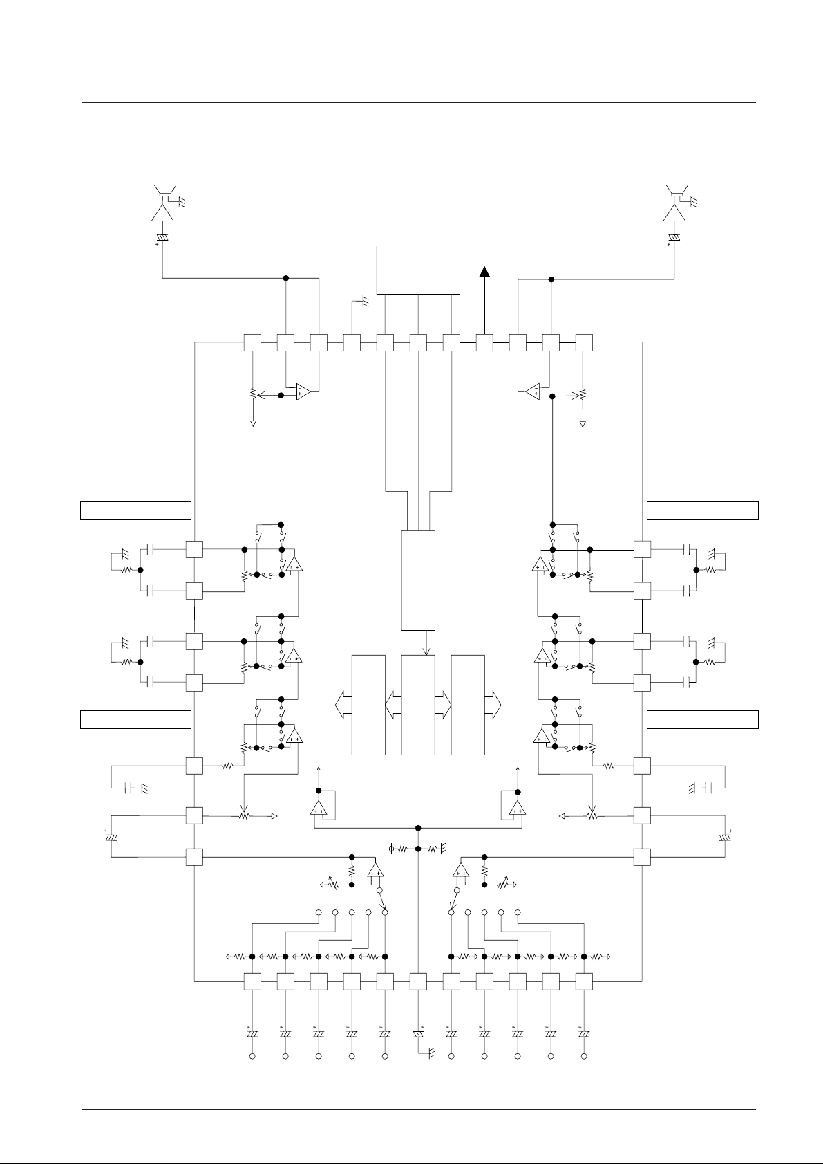
Pin Functions
Pin No. Pin Name Function Equivalent circuit
• Input signal pins
18
17
16
15
14
20
21
22
23
24
L1
L2
L3
L4
L5
R1
R2
R3
R4
R5
VDD
VDD
SEL0
Ln
Rn
Vref
VDD
BASS1
SB
BASS2
• Input selector output pins
13
25
LSEL0
RSEL0
• Capacitor and resistor connection pins for configuring filter,
used for bass and super bass band, or for mid and bass
10
9
28
29
8
30
LBASS1
LBASS2
RBASS1
RBASS2
LSB
RSB
VDD
OUT
• ATT + equalizer output pins/capacitor connection pins used
to configure super bass filter
7
31
LOUT
ROUT
VDD
VRIN
• Volume input pins
12
26
LVRIN
RVRIN
VDD
TRE
• Capacitor connection pins for configuring treble band filter
11
27
LTRE
RTRE
Continued on next page.
Page 14

No. 6867-14/28
LC75343M
Continued from preceding page.
Pin No. Pin Name Function Equivalent circuit
• Connect a capacitor of a few tens of µF between Vref and
AV
SS(VSS
) as a analog ground 0.5 × VDDvoltage
generator, current ripple countermeasure.
19 Vref
VDD
Vref
VDD
• Ground pin 3
V
SS
• Power supply pin35
V
DD
• Chip enable pin
Data is written to the internal latch and the analog switches
are operated when the level changes from high to low.
Data transfer is enabled when the level is high.
2CE
VDD
INP
Vref
• General-purpose op-amp specifications
Non-inverted input pins of general-purpose op-amp
When not used, leave open.
• ATT control specifications
Non-inverted input pins for ATT.
• 3-band specifications
Non-inverted input pins for ATT.
Always leave these pins open.
6
32
LINP
RINP
VDD
INM
• General-purpose op-amp specifications
Non-inverted input pins of general-purpose op-amp.
When not used, connect these pins to the L(R)
OPOUT
pins.
(Connected between pin 5 and pin 4)
(Connected between pin 33 and pin 34)
• ATT control specifications
Op-amp inverted input pins for ATT.
Connected to L(R) OPOUT pins.
(Connected between pin 5 and pin 4)
(Connected between pin 33 and pin 34)
• 3-band specifications
Inverted input pins of ATT op-amp.
Connected to L(R) OPOUT pins.
(Connected between pin 5 and pin 4)
(Connected between pin 33 and pin 34)
5
33
LINM
RINM
VDD
OPOUT
• General-purpose op-amp specifications
General-purpose op-amp output pins.
When not used, connect these pins to the L(R) INM pins.
(Connected between pin 5 and pin 4)
(Connected between pin 33 and pin 34)
• ATT control specifications
Op-amp output pins for ATT.
Connected to L(R) INM pins.
(Connected between pin 5 and pin 4)
(Connected between pin 33 and pin 34)
• 3-band specifications
ATT op-amp output pins.
(Connected to L(R) INM pins.
(Connected between pin 5 and pin 4)
(Connected between pin 33 and pin 34)
4
34
LOPOUT
ROPOUT
• Serial data pins and clock input pin for control
1
36
DI
CL
Page 15

No. 6867-15/28
LC75343M
Equivalent Circuit
• Selector Block/Reference Voltage Generator
VDD
LVref
LVref
Total = 6 k
20 k
20 k
VREF
L1
L2
L3
L4
L5
50 k
LVref
Equivalent to right channel
Unit: (resistance: Ω)
50 k
50 k
50 k
50 k
0 dB
2 dB
4 dB
6 dB
8 dB
10 dB
12 dB
14 dB
16 dB
18 dB
20 dB
22 dB
24 dB
26 dB
28 dB
30 dB
R1
R2
R3
R4
R5
R6
R7
R8
R9
R10
R11
R12
R13
R14
R15
R16
1.234 k
0.980 k
0.779 k
0.618 k
0.491 k
0.390 k
0.310 k
0.246 k
0.196 k
0.155 k
0.123 k
0.098 k
0.078 k
0.062 k
0.049 k
0.190 k
LSEL0
Page 16

No. 6867-16/28
LC75343M
• Treble/Bass/Super Bass Band
From
volume
block
Equivalent to right channel
Unit: (resistance: Ω)
SW3
LTRE
LBASS1
Total = 51.701 k
Total = 33.097 k
LBASS2
LOPOUT
LINM
LINP
↑
Common to general-purpose
op-amp, ATT op-amp
Equivalent to right channel
Unit: (resistance: Ω)
LVREF
SW4
SW2
SW1
±10 dB16.240 k
±8 dB
±6 dB
±4 dB
±2 dB
0 dB
4.246 k
5.346 k
6.730 k
8.473 k
10.666 k
SW3
SW4
SW2
SW1
±10 dB
±8 dB
±6 dB
±4 dB
±2 dB
0 dB
3.964 k
4.989 k
6.281 k
7.908 k
9.955 k
LSB
Total = 33.097 k
LOUT
SW3
SW4
SW2
SW1
±10 dB
±8 dB
±6 dB
±4 dB
±2 dB
0 dB
3.964 k
4.989 k
6.281 k
7.908 k
9.955 k
During boost, SW1 and SW3 are on, during cut, SW2 and SW4 are on, when 0 dB, 0dBSW and SW2 and SW3 are on.
For the super bass block:
• In case of general-purpose op-amp specifications, ATT control specifications (“0” set to D3)
SW3, SW4 are off, and only boost side operates (only SW1 is on).
• In case of 3-band specifications ( “1” set to D3)
During boost, SW1 and SW3 are on, during cut, SW2 and SW4 are on, when 0 dB, 0dBSW and SW2 and SW3 are
on.
Page 17

No. 6867-17/28
LC75343M
• Volume Block
LVRIN
R1 = 5434
R2 = 4845
R3 = 4319
R4 = 3850
R5 = 3431
R6 = 3058
R7 = 2726
R8 = 2429
R9 = 2165
R10 = 1930
R11 = 1720
R12 = 1533
R13 = 1366
R14 = 1218
R15 = 1085
R16 = 967
R17 = 862
R18 = 768
R19 = 685
R20 = 610
R21 = 544
R22 = 485
R23 = 432
R24 = 385
R25 = 343
R26 = 306
R27 = 273
0 dB
–1 dB
–2 dB
–3 dB
–4 dB
–5 dB
–6 dB
–7 dB
–8 dB
–9 dB
–10 dB
–11 dB
–12 dB
–13 dB
–14 dB
–15 dB
–16 dB
–17 dB
–18 dB
–19 dB
–20 dB
–21 dB
–22 dB
–23 dB
–24 dB
–25 dB
–26 dB
–27 dB
R28 = 243
R29 = 216
R30 = 193
R31 = 172
R32 = 153
R33 = 137
R34 = 122
R35 = 108
R36 = 97
R37 = 86
R38 = 77
R39 = 68
R40 = 61
R41 = 54
R42 = 48
R43 = 86
R44 = 77
R45 = 69
R46 = 61
R47 = 55
R48 = 49
R49 = 87
R50 = 77
R51 = 130
R52 = 104
–28 dB
–29 dB
–30 dB
–31 dB
–32 dB
–33 dB
–34 dB
–35 dB
–36 dB
–37 dB
–38 dB
–39 dB
–40 dB
–41 dB
–42 dB
–43 dB
–44 dB
–45 dB
–46 dB
–47 dB
–48 dB
–49 dB
–50 dB
–52 dB
–54 dB
R53 = 164
R54 = 130
R55 = 104
R56 = 165
R57 = 131
R58 = 104
R59 = 165
R60 = 131
R61 = 104
R62 = 175
R63 = 235
R64 = 403
To
treble
block
–56 dB
–58 dB
–60 dB
–62 dB
–64 dB
–66 dB
–68 dB
–70 dB
–74 dB
–78 dB
–∞ dB
LVref
Equivalent to right channel
Unit: (resistance: Ω)
R81 = 794
R82 = 796
R83 = 798
R84 = 800
R85 = 802
R86 = 804
Page 18

No. 6867-18/28
LC75343M
• ATT Block Equivalent Circuit
(during ATT control)
LINP
To ATT op-amp
Total = 50.000 k
Equivalent to right channel
Unit: (resistance: Ω)
R1 = 10.279 k
R2 = 8.169 k
R3 = 6.489 k
R4 = 5.155 k
R5 = 4.095 k
R6 = 3.253 k
R7 = 2.584 k
R8 = 2.052 k
R9 = 1.630 k
R10 = 6.295 k
0 dB
–2 dB
–4 dB
–6 dB
–8 dB
–10 dB
–12 dB
–14 dB
–16 dB
–18 dB
– ∞
Page 19

No. 6867-19/28
LC75343M
Test Circuit
General-Purpose Op-amp Specifications
• Total Harmonic Distortion
µCOM
VDD
2.2 µ
2.2 µ
7.6 k
7.6 k
Equivalent to right channel
Units: resistance: Ω, capacitance: F
S.G Distortion analyzer
LC75343M
THDin
7.6 k
7.6 k
0.1 µ
0.1 µ
0.1 µ
0.1 µ
2700p
1 µ
1 µ
1 µ
1 µ
1 µ
1 µ
0.1 µ
0.1 µ
0.1 µ
0.1 µ
2700p
1 µ
1 µ
1 µ
1 µ
1 µ
1 µ
22 µ
36
35
34
33
32
31
30
29
28
27
26
25
24
23
22
21
20
19
1
2
3
4
5
6
7
8
9
10
11
12
13
14
15
16
17
18
Page 20

No. 6867-20/28
LC75343M
• Output Noise Voltage
µCOM
VDD
2.2 µ
2.2 µ
7.6 k
7.6 k
Equivalent to right channel
Units: resistance: Ω, capacitance: F
LC75343M
7.6 k
1 k × 5
7.6 k
0.1 µ
0.1 µ
0.1 µ
0.1 µ
2700p
1 µ
1 µ
1 µ
1 µ
1 µ
1 µ
0.1 µ
0.1 µ
0.1 µ
0.1 µ
2700p
1 µ
1 µ
1 µ
1 µ
1 µ
1 µ
22 µ
36
35
34
33
32
31
30
29
28
27
26
25
24
23
22
21
20
19
1
2
3
4
5
6
7
8
9
10
11
12
13
14
15
16
17
18
Noise meter
Page 21

No. 6867-21/28
LC75343M
• Crosstalk
µCOM
VDD
2.2 µ
2.2 µ
7.6 k
7.6 k
Equivalent to right channel
Units: resistance: Ω, capacitance: F
LC75343M
7.6 k
1 k × 5
7.6 k
0.1 µ
0.1 µ
0.1 µ
0.1 µ
2700p
1 µ
1 µ
1 µ
1 µ
1 µ
1 µ
0.1 µ
0.1 µ
0.1 µ
0.1 µ
2700p
1 µ
1 µ
1 µ
1 µ
1 µ
1 µ
22 µ
36
35
34
33
32
31
30
29
28
27
26
25
24
23
22
21
20
19
1
2
3
4
5
6
7
8
9
10
11
12
13
14
15
16
17
18
Volt meter S.G
Page 22

No. 6867-22/28
LC75343M
ATT Control Specifications and 3-Band Specifications
• Total Harmonic Distortion
µCOM
VDD
2.2 µ
2.2 µ
7.6 k
7.6 k
Equivalent to right channel
Units: resistance: Ω, capacitance: F
S.G Distortion analyzer
LC75343M
THDin
7.6 k
7.6 k
1 µ
0.1 µ
0.1 µ
0.1 µ
0.1 µ
2700p
1 µ
1 µ
1 µ
1 µ
1 µ
1 µ
36
35
34
33
32
31
30
29
28
27
26
25
24
23
22
21
20
19
1
2
3
4
5
6
7
8
9
10
11
12
13
14
15
16
17
18
1 µ
0.1 µ
0.1 µ
0.1 µ
0.1 µ
2700p
1 µ
1 µ
1 µ
1 µ
1 µ
1 µ
22 µ
Page 23

No. 6867-23/28
LC75343M
• Output Noise Voltage
µCOM
VDD
2.2 µ
2.2 µ
7.6 k
7.6 k
Equivalent to right channel
Units: resistance: Ω, capacitance: F
S.G Distortion analyzer
LC75343M
THDin
7.6 k
7.6 k
1 µ
0.1 µ
0.1 µ
0.1 µ
0.1 µ
2700p
1 µ
1 µ
1 µ
1 µ
1 µ
1 µ
36
35
34
33
32
31
30
29
28
27
26
25
24
23
22
21
20
19
1
2
3
4
5
6
7
8
9
10
11
12
13
14
15
16
17
18
1 µ
0.1 µ
0.1 µ
0.1 µ
0.1 µ
2700p
1 µ
1 µ
1 µ
1 µ
1 µ
1 µ
22 µ
Page 24

No. 6867-24/28
LC75343M
• Crosstalk
µCOM
VDD
2.2 µ
2.2 µ
7.6 k
7.6 k
Equivalent to right channel
Units: resistance: Ω, capacitance: F
LC75343M
7.6 k
7.6 k
1 µ
0.1 µ
0.1 µ
0.1 µ
0.1 µ
2700p
1 µ
1 µ
1 µ
1 µ
1 µ
1 µ
36
35
34
33
32
31
30
29
28
27
26
25
24
23
22
21
20
19
1
2
3
4
5
6
7
8
9
10
11
12
13
14
15
16
17
18
Noise meter
1 k × 5
S.G
1 µ
0.1 µ
0.1 µ
0.1 µ
0.1 µ
2700p
1 µ
1 µ
1 µ
1 µ
1 µ
1 µ
22 µ
Page 25

Calculation of External Equalizer Constant
Bass/Super Bass Circuit
The equivalent circuit and the formula for calculating the external RC with a mean frequency of 1000 Hz are shown
below.
• Bass/super bass band equivalent circuit block diagram
• Calculation example
Specification Mean frequency: f0 = 1000 Hz
Gain during maximum boost: G = 10 dB
Using R1 = 0, R2 = 33.097 kΩ, and C1 = C2 = C,
We obtain R2 from G = 10 dB.
We obtain C from mean frequency f0 = 1000 Hz.
We obtain Q.
No. 6867-25/28
LC75343M
C1
R1 R2
R3
C2
G
+10 dB
= 20 × LOG10 1 +
R2
2R3
R3 =
R2
2 10
G+10dB/20
–1
33097
2
× (3.162 – 1)
=≠ 7.6 KΩ
f 0 =
R3R2C1C2
1
2π
C ==
1
2
πf0 R3R2
1
2π × 1000 33097 × 7600
≠ 0.01 µF
Q =
R3R2
R3R2
2R3
1
≠ 1.04
Page 26

Treble Band Circuit
The shelving characteristics can be obtained for the treble band.
The equivalent circuit and calculation formula during boost are indicated below.
• Calculation example
Specification Set frequency: f = 26000 Hz
Gain during maximum boost: G
+10 dB
= 10 dB
Using R1 = 16.240 kΩ and R2 = 35.461 kΩ, and inserting the above values in the following formula, we
obtain:
No. 6867-26/28
LC75343M
C
R1 R2
C =
R2
)
2
– R1
2
1
2
πf
10
G/20
– 1
(
=
1
2
π26000
35461
3.16–1
≠ 2700(pF)
()
2
– 16240
2
R2
R1
2
+ (1 / ωC)
2
G = 20 × LOG10 1 +
Usage Cautions
• Upon power application, the internal analog switch status is undefined. Use an external countermeasure such as
muting until data is set.
• When performing initial setting after applying power, send the initial setting data for the left and right channels
prior to canceling mute.
• To ensure that the high-frequency digital signals sent to the CL, DI, and CE pins do not spill over to the analog
signal block, either guard these signal lines with a ground pattern, or perform transmission using shielded wires.
Page 27

No. 6867-27/28
LC75343M
Volume Control Step Characteristics Bass Band Frequency Characteristics
Middle Band Frequency Characteristics
Volume Attenuation — dB
Step setting — dB
Super Bass Band Frequency Characteristics
Treble Band Frequency Characteristics
Gain, G — dBVGain, G — dBV
Gain, G — dBV Gain, G — dBV
Frequency, f — Hz
Frequency, f — Hz
Frequency, f — Hz
Frequency, f — Hz
Frequency, f — Hz
THD — Frequency Characteristics (1)
Total harmonic distortion, THD — %
Frequency, f — Hz
THD — Frequency Characteristics (2)
Total harmonic distortion, THD — %
Supply voltage, VDD — V
THD — Supply Voltage Characteristics (1)
Total harmonic distortion, THD — %
General-purpose op-amp specifications
ATT control specifications and
3-band specifications
ATT control specifications and
3-band specifications
Page 28

PS No. 6867-28/28
LC75343M
This catalog provides information as of February, 2001. Specifications and information herein are subject
to change without notice.
Specifications of any and all SANYO products described or contained herein stipulate the performance,
characteristics, and functions of the described products in the independent state, and are not guarantees
of the performance, characteristics, and functions of the described products as mounted in the customer’s
products or equipment. To verify symptoms and states that cannot be evaluated in an independent device,
the customer should always evaluate and test devices mounted in the customer’s products or equipment.
SANYO Electric Co., Ltd. strives to supply high-quality high-reliability products. However, any and all
semiconductor products fail with some probability. It is possible that these probabilistic failures could
give rise to accidents or events that could endanger human lives, that could give rise to smoke or fire,
or that could cause damage to other property. When designing equipment, adopt safety measures so
that these kinds of accidents or events cannot occur. Such measures include but are not limited to protective
circuits and error prevention circuits for safe design, redundant design, and structural design.
In the event that any or all SANYO products (including technical data, services) described or contained
herein are controlled under any of applicable local export control laws and regulations, such products must
not be exported without obtaining the export license from the authorities concerned in accordance with the
above law.
No part of this publication may be reproduced or transmitted in any form or by any means, electronic or
mechanical, including photocopying and recording, or any information storage or retrieval system,
or otherwise, without the prior written permission of SANYO Electric Co., Ltd.
Any and all information described or contained herein are subject to change without notice due to
product/technology improvement, etc. When designing equipment, refer to the “Delivery Specification”
for the SANYO product that you intend to use.
Information (including circuit diagrams and circuit parameters) herein is for example only; it is not
guaranteed for volume production. SANYO believes information herein is accurate and reliable, but
no guarantees are made or implied regarding its use or any infringements of intellectual property rights
or other rights of third parties.
THD — Supply Voltage Characteristics (2)
General-purpose op-amp
specifications
Total harmonic distortion, THD — %
Supply voltage, VDD — V
THD — Input Level Characteristics (2)
General-purpose op-amp
specifications
THD — Input Level Characteristics (1)
ATT control specifications and
Total harmonic distortion, THD — %
3-band specifications
Input level, V
— dBV
IN
Total harmonic distortion, THD — %
Input level, VIN — dBV
 Loading...