

Page 1
Ordering number : EN5913
101698RM (OT) No. 5913-1/10
Overview
The LC75281E is a four-band stereo parametric equalizer.
A parametric equalizer is a fully general equalizer that
allows all three parameters that define an equalizer’s
characteristics, i.e., the center frequency, gain, and Q, to
be set independently.
Functions
• Four-band (low, low mid, high mid, and high) left and
right channels parametric equalizer
• For each band:
Center frequency: 11 positions
Gain: 13 positions in ±2dB steps
Q: Variable over 8 positions
• The center frequency, gain, and Q control settings are
set using serial data input in the CCB format.
Features
• A parametric equalizer with the following features can
be implemented with just two ICs: this IC and a
microcontroller.
• The center frequency, gain, and Q can be controlled by a
single operation.
• Memory recall by a single operation can be implemented using preset values.
• Either shelving or peaking characteristics can be
selected for the low band.
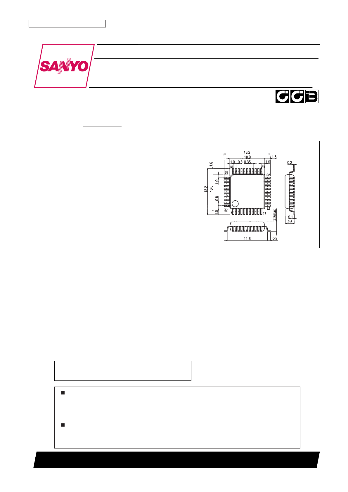
Package Dimensions
unit: mm
3159-QFP64E
LC75281E
SANYO Electric Co.,Ltd. Semiconductor Bussiness Headquarters
TOKYO OFFICE Tokyo Bldg., 1-10, 1 Chome, Ueno, Taito-ku, TOKYO, 110-8534 JAPAN
Parametric Equalizer System
CMOS IC
Any and all SANYO products described or contained herein do not have specifications that can handle
applications that require extremely high levels of reliability, such as life-support systems, aircraft’s
control systems, or other applications whose failure can be reasonably expected to result in serious
physical and/or material damage. Consult with your SANYO representative nearest you before using
any SANYO products described or contained herein in such applications.
SANYO assumes no responsibility for equipment failures that result from using products at values that
exceed, even momentarily, rated values (such as maximum ratings, operating condition ranges, or other
parameters) listed in products specifications of any and all SANYO products described or contained
herein.
SANYO: QFP64E (QIP64E)
[LC75281E]
• CCB is a trademark of SANYO ELECTRIC CO., LTD.
• CCB is SANYO’s original bus format and all the bus
addresses are controlled by SANYO.
Page 2
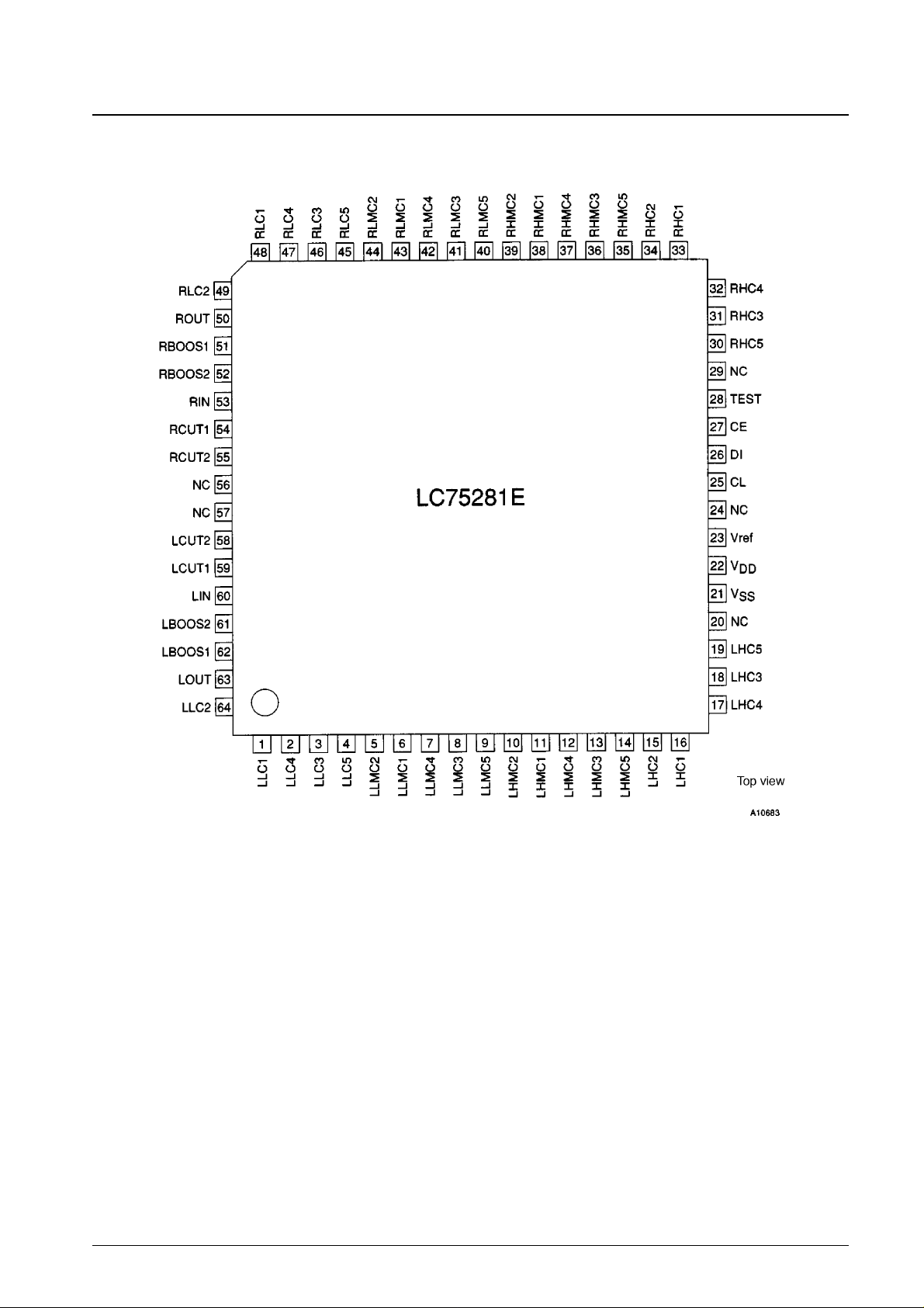
Pin Assignment
No. 5913-2/10
LC75281E
Page 3

Specifications
Absolute Maximum Ratings at Ta = 25°C, VSS= 0 V
Allowable Operating Ranges at Ta = –40 to +85°C, VSS= 0 V
Electrical Characteristics at Ta = 25°C, f = 1 kHz, VDD= 8 V, VSS= 0 V
Pin Functions
No. 5913-3/10
LC75281E
Parameter Symbol Conditions Ratings Unit
Maximum supply voltage V
DD
max 10.5 V
Maximum input voltage
V
IN
1 max LIN, RIN 0 to V
DD
V
V
IN
2 max CL, CE, DI 0 to V
DD
V
Allowable power dissipation Pd max Ta ≤ 85°C 300 mW
Operating temperature Topr –40 to +85 °C
Storage temperature Tstg –50 to +125 °C
Parameter Symbol Conditions
Ratings
Unit
min typ max
Supply voltage V
DD
6.0 9.0 V
High-level input voltage V
IH
CL, CE, DI 4.0 V
DD
V
Low-level input voltage V
IL
CL, CE, DI V
SS
1.0 V
Input voltage range V
IN
LIN, RIN 0 V
DD
V
Load resistance R
L
LOUT, ROUT, MIXOUT 1 kΩ
Input pulse width tøw CL 1 µs
Setup time tsetup CL, CE, DI 1 µs
Hold time thold CL, CE, DI 1 µs
Operating frequency fopg CL 500 kHz
Parameter Symbol Conditions
Ratings
Unit
min typ max
Current drain I
DD
V
DD
36 50 mA
Output voltage V
O
LOUT, ROUT: THD = 1% 2.2 Vrms
THD1 LOUT, ROUT: Vo = Flat, V
IN
= 0 dBV 0.005 0.01 %
Total harmonic distortion
THD2
LOUT, ROUT: Vo = Boost,
0.1 1 %
All bands +2 dB, V
IN
= –15 dBV
V
N
1
LOUT, ROUT: Vo = Flat,
7 15 µs
Rg = 1 kΩ, IHF-A filters
V
N
2
LOUT, ROUT: Vo = Flat,
13 µs
Rg = 1 kΩ, DIN filters
LOUT, ROUT, Rg = 1 k
Ω, f0 = f1, Q = Q1
Output noise voltage
V
N
3
IHF-A filter, all bands at full boost, with the external
58 µs
constants the same as those for the center
frequency (example 1)
LOUT, ROUT, Rg = 1 kΩ, f0 = f1, Q = Q1
V
N
4
IHF-A filters, all bands at full cut, with the external
23 µs
constants the same as those for the center frequency
(example 1)
Crosstalk between inputs CT V
IN
= 1 Vrms, f = 1 kHz 60 80 dB
High-level input current I
IH
CL, DI, CE, VIN= 9 V 1 µA
Low-level input current I
IL
CL, DI, CE, VIN= 0 V –1 µA
All bands
DC variation V
DC
G = +12 dB, Q: Setting switched from Q1 to Q2
–10 +10 mV
With the external constants the same as those for the
center frequency (example 1) shown on page 7.
Pin No. Pin Function
64 LLC2
1 LLC1
2 LLC4
3 LLC3
4 LLC5
5 LLMC2
6 LLMC1
7 LLMC4
8 LLMC3
Left channel low band control block.
External capacitor connections.
Left channel low mid band control block.
External capacitor connections.
Continued on next page.
Page 4

Continued from preceding page.
No. 5913-4/10
LC75281E
Pin No. Pin Function
10 LHMC2
11 LHMC1
12 LHMC4
13 LHMC3
14 LHMC5
15 LHC2
16 LHC1
17 LHC4
18 LHC3
19 LHC5
20, 24, 29
NC Unused pins. These pins must be either left open or connected to V
SS
.
56, 57
23 Vref
Internal operational amplifier reference voltage generator outputs.
Several capacitors with values of about 10 µF must be connected with this pin to reduce ripple.
21 V
SS
Power supply.
22 V
DD
These pins must be connected to the stipulated power supply.
27 CE
26 DI
Serial data and clock inputs for IC control
25 CL
49 RLC2
48 RLC1
47 RLC4
46 RLC3
45 RLC5
44 RLMC2
43 RLMC1
42 RLMC4
41 RLMC3
40 RLMC5
39 RHMC2
38 RHMC1
37 RHMC4
36 RHMC3
35 RHMC5
34 RHC2
33 RHC1
32 RHC4
31 RHC3
30 RHC5
58 LCUT2
59 LCUT1
61 LBOOS2
62 LBOOS1
55 RCUT2
54 RCUT1
52 RBOOS2
51 RBOOS1
60 LIN Left channel audio signal input (Must be driven with a low load capacitance.)
53 RIN Right channel audio signal input (Must be driven with a low load capacitance.)
63 LOUT Left channel audio signal output (Must be received with a low load capacitance.)
50 ROUT Right channel audio signal output (Must be received with a low load capacitance.)
28 TEST
IC test pin.
This pin must be left open when not used for IC test.
Left channel high mid band control block.
External capacitor connections.
Left channel high band control block.
External capacitor connections.
Chip enable input. Data is written to the internal latch and the analog switches operate when this pin
changes from high to low. Data transfer is enabled when this pin is high.
Right channel low band control block.
External capacitor connections.
Right channel low mid band control block.
External capacitor connections.
Right channel high mid band control block.
External capacitor connections.
Right channel high band control block.
External capacitor connections.
Internal filter DC offset voltage exclusion capacitor connections.
Capacitors of about 10 µF must be connected between pins 61 and 62, and between pins 63 and 64.
(These are for the left channel block.)
Internal filter DC offset voltage exclusion capacitor connections.
Capacitors of about 10 µF must be connected between pins 51 and 52, and between pins 49 and 50.
(These are for the right channel block.)
Page 5

Block Diagram
No. 5913-5/10
LC75281E
Low band
Low mid band
High mid band
High band
The blocks enclosed in dotted
lines are identical.
Page 6

• Center frequency (fo)
External capacitor calculations
Figure a shows the LC75281E internal f0 control circuit. The center frequency f0 can be set to one of 11 frequencies in
1/3 octave steps by switching the resistors in the figure.
The value of the external capacitor C is determined by substituting the desired center frequency in the following formula.
fo max: Corresponds to 315 Hz in the low band row in the preceding table.
• Gain: 13 positions in 2-dB steps
• Q
No. 5913-6/10
LC75281E
Band f1 f2 f3 f4 f5 f6 f7 f8 f9 f10 f11 External capacitor (µF)
Low 31.5 40 50 63 80 100 125 160 200 250 315 0.047
Low mid 160 200 250 315 400 500 630 800 1 k 1.25 k 1.6 k 0.0094
High mid 630 800 1 k 1.25 k 1.6 k 2 k 2.5 k 3.15 k 4 k 5 k 6.3 k 0.00235
High 1.6 k 2 k 2.5 k 3.15 k 4 k 5 k 6.3 k 8 k 10 k 12.5 k 16 k 0.0094
Cf =
1
•
Rb//Rf
2π Rf fo max Ra + (Rb//Rf)
Q1 Q2 Q3 Q4 Q5 Q6 Q7 Q8
Q 0.404 0.667 1.41 2.15 2.87 4.32 5.76 8.65
OCT 3 2 1 2/3 1/2 1/3 1/4 1/6
Figure a
Equivalent Circuit for Cf calculation
Page 7

Data Input Procedure
The LC75281E is controlled by inputting the stipulated serial data to the CE, CL, and DI pins. The data consists of
28 bits, of which 8 bits are the address and 20 bits are the data.
Note *: The 2× command doubles the center frequency of all bands. When setting this bit to 1, applications must either enter the band data for one of the
bands in bits D1 to D19, or must set both bits D4 and D5 to 0, in which case all other bits are ignored.
Normal
2×
: Low (Peaking)
: Low mid (Peaking)
: High mid (Peaking)
: Low (Shelving)
No. 5913-7/10
LC75281E
Address code
Normal/2× control
*
Channel selection
Center frequency setting Gain setting
Q setting
Left and right
Band selection and
peaking/shelving selection
≤
Page 8

Sample Application Circuit
No. 5913-8/10
LC75281E
Page 9

No. 5913-9/10
LC75281E
Gain Characteristics (Peaking) Gain Characteristics (Shelving)
Frequency, f — Hz
Q Characteristics (Peaking)
Frequency, f — Hz
Q Characteristics (Shelving) - 1
Frequency, f — Hz
Q Characteristics (Shelving) - 2
Frequency, f — Hz
Center Frequency Characteristics (Shelving)
Frequency, f — Hz
Frequency, f — Hz
Center Frequency Characteristics (Peaking)
Frequency, f — Hz
Output level — dB
Output level — dB
Output level — dB
Output level — dB
Output level — dB
Output level — dB
Output level — dB
Low band
Vin = –20 dB V
External capacitor: Cf = 0.047 µF
Settings: f0 = f11
Q = Q1
Low band
Vin = –20 dB V
External capacitor: Cf = 0.047 µF
Settings: G = ±12 dB
Q = Q1
Low band
Vin = –20 dB V
External capacitor: Cf = 0.047 µF
Settings: f0 = f11
Q = Q1
Low band
Vin = –20 dB V
External capacitor:
Cf = 0.047 µF
Settings: f0 = f11
G = –12 dB
Low mid band
Vin = –20 dB V
External capacitor: Cf = 0.01 µF
Settings: G = ±12 dB
Q = Q4
High mid band
Vin = –20 dB V
External capacitor: Cf = 0.0022 µF
Settings: f0 = f17
G = ±12 dB
Low band
Vin = –20 dB V
External capacitor:
Cf = 0.047 µF
Settings: f0 = f11
Q = Q1
Page 10

No. 5913-10/10
LC75281E
This catalog provides information as of October, 1998. Specifications and information herein are subject
to change without notice.
Specifications of any and all SANYO products described or contained herein stipulate the performance,
characteristics, and functions of the described products in the independent state, and are not guarantees
of the performance, characteristics, and functions of the described products as mounted in the customer’s
products or equipment. To verify symptoms and states that cannot be evaluated in an independent device,
the customer should always evaluate and test devices mounted in the customer’s products or equipment.
SANYO Electric Co., Ltd. strives to supply high-quality high-reliability products. However, any and all
semiconductor products fail with some probability. It is possible that these probabilistic failures could
give rise to accidents or events that could endanger human lives, that could give rise to smoke or fire,
or that could cause damage to other property. When designing equipment, adopt safety measures so
that these kinds of accidents or events cannot occur. Such measures include but are not limited to protective
circuits and error prevention circuits for safe design, redundant design, and structural design.
In the event that any and all SANYO products described or contained herein fall under strategic
products (including services) controlled under the Foreign Exchange and Foreign Trade Control Law of
Japan, such products must not be exported without obtaining export license from the Ministry of
International Trade and Industry in accordance with the above law.
No part of this publication may be reproduced or transmitted in any form or by any means, electronic or
mechanical, including photocopying and recording, or any information storage or retrieval system,
or otherwise, without the prior written permission of SANYO Electric Co., Ltd.
Any and all information described or contained herein are subject to change without notice due to
product/technology improvement, etc. When designing equipment, refer to the “Delivery Specification”
for the SANYO product that you intend to use.
Information (including circuit diagrams and circuit parameters) herein is for example only; it is not
guaranteed for volume production. SANYO believes information herein is accurate and reliable, but
no guarantees are made or implied regarding its use or any infringements of intellectual property rights
or other rights of third parties.
 Loading...