

Page 1
Overview
The LC7527E is a microprocessor controllable seven-band
graphic equalizer LSI that does not require the use of
external semiconductor inductors (simulated inductors).
Functions
• Left and right channel seven-band graphic equalizers
• Each band operates in ±2 dB steps.
• Each band has a maximum boost of +12 dB and a
maximum cut of –12 dB for a total of 13 settings.
• Independent left and right channel operation
• Serial data input supports CCB format communications
with the system controller.
• CMOS LSI with a 12 V breakdown voltage
Features
• This LSI, in conjunction with a control microprocessor,
can implement in two chips, an electronic graphic
equalizer with the following features.
— One touch gain control for each band
— One touch memory setting recall allows users to
select desired frequency characteristics for each
track.
— Since the LC7527E includes band filter amplifiers
on chip, capacitors are the only external components
required in application systems.
— Minimal switching noise due to the use of a Silicon
gate CMOS process.
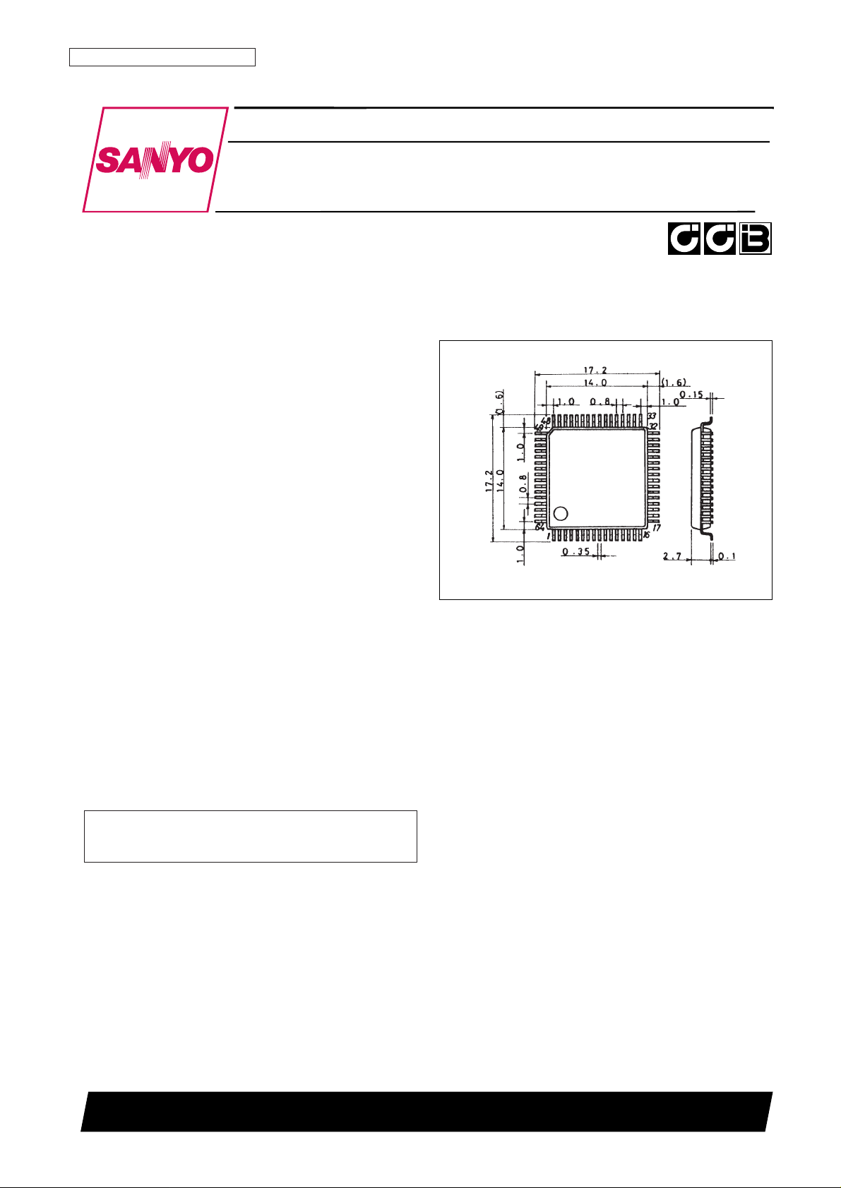
Package Dimensions
unit: mm
3159-QFP64E
CMOS LSI
O3096HA(OT)/90894TH (OT) 4466-1/11
SANYO: QFP64E
[LC7527E]
SANYO Electric Co.,Ltd. Semiconductor Bussiness Headquarters
TOKYO OFFICE Tokyo Bldg., 1-10, 1 Chome, Ueno, Taito-ku, TOKYO, 110 JAPAN
Graphic Equalizer System
LC7527E
Ordering number : EN4466B
• CCB is a trademark of SANYO ELECTRIC CO., LTD.
• CCB is SANYO’s original bus format and all the bus
addresses are controlled by SANYO.
Page 2
No. 4466-2/11
LC7527E
Parameter Symbol Conditions Ratings Unit
Maximum supply voltage V
DD-VEE
max AVDD, AVEE, DVDD, DVEE* 12 V
V
IN
max1 CL, DI, CE VSS– 0.3 to VDD+ 0.3 V
Maximum input voltage V
IN
max2 LIN1, LIN2, RIN1, RIN2 VEE– 0.3 to VDD+ 0.3 V
V
IN
max3 S1 VEE– 0.3 to VDD+ 0.3 V
Allowable power dissipation Pd max Ta ≤ 85°C 280 mW
Operating temperature Topr –40 to +85 °C
Storage temperature Tstg –50 to +125 °C
Specifications
Absolute Maximum Ratings at Ta = 25°C, VSS= 0 V
Note: * –6 V ≤ VEE≤ VSS≤ V
DD
Parameter Symbol Conditions
Ratings
Unit
min typ max
V
DD
AVDD, DV
DD
5 V
Supply voltage V
EE
AVEE, DV
EE
–5 V
V
DD-VEEAVDD
, AVEE, DVDD, DV
EE
8.0 11.0 V
Input high level voltage V
IH
CL, DI, CE 3.0 V
DD
V
Input low level voltage V
IL
CL, DI, CE V
SS
1.0 V
Input amplitude voltage
V
IN
1 LIN1, LIN2, RIN1, RIN2 V
EE
V
DD
Vp-p
V
IN
2 S1 V
EE
V
DD
V
Clock pulse width t
øW
CL 1 µs
Setup time tsetup CL, DI, CE 1 µs
Hold time t
HOLD
CL, DI, CE 1 µs
Operating frequency fopg CL 500 kHz
Allowable Operating Ranges at Ta = 25°C, VSS= 0 V
Parameter Symbol Conditions
Ratings
Unit
min typ max
THD (1) V
OUT
= 1 Vrms, FLAT, f = 20 kHz 0.01 0.05 %
THD (2) V
OUT
= 1 Vrms, FLAT, f = 1 kHz 0.001 0.005 %
Total harmonic distortion
THD (3)
V
OUT
= 300 mVrms, FLAT, f = 20 kHz
0.042 0.2 %
with all bands at full boost
THD (4)
V
OUT
= 300 mVrms, FLAT, f = 1 kHz
0.045 0.2 %
with all bands at full boost
Crosstalk CT V
OUT
= 1 Vrms, f = 20 kHz, FLAT, Rg = 1 kΩ 58 dB
Setting error ∆B with other bands flat –2 +2 dB
Current drain I
DD
VDD-VEE= 11 V 30 mA
Analog switch off leakage current I
OFF
LIN1, LIN2, RIN1, RIN2 10 µA
Electrical Characteristics at Ta = 25°C, VDD= 5 V, VEE= –5 V, VSS= 0 V
Page 3
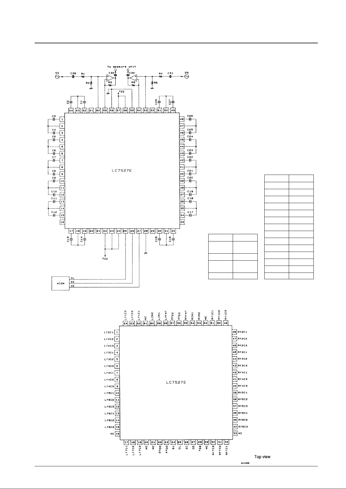
Electrical Characteristics Test Circuit
Pin Assignment
No. 4466-3/11
LC7527E
No. Unit (F)
C29, C30,
10 µ
C31, C32
No. Unit (Ω)
R1, R3,
7.5 k
R4, R6
R2, R5 1 M
No. Unit (F)
C1, C28 0.94 µ
C2, C27 0.034 µ
C3, C26 0.377 µ
C4, C25 0.0133 µ
C5, C24 0.1506 µ
C6, C23 5390 p
C7, C22 0.057 µ
C8, C21 2156 p
C9, C20 0.0242 µ
C10, C19 867 p
C11, C18 9200 p
C12, C17 3322 p
C13, C16 3770 p
C14, C15 1330 p
Page 4
No. 4466-4/11
LC7527E
Pin Functions
Pin Pin No. Circuit type Function
Lf1C1
Lf1C2
Lf1C3
Rf1C1
Rf1C2
Rf1C3
Lf2C1
Lf2C2
Lf2C3
Rf2C1
Rf2C2
Rf2C3
Lf3C1
Lf3C2
Lf3C3
Rf3C1
Rf3C2
Rf3C3
Lf4C1
Lf4C2
Lf4C3
Rf4C1
Rf4C2
Rf4C3
Lf5C1
Lf5C2
Lf5C3
Rf5C1
Rf5C2
Rf5C3
Lf6C1
Lf6C2
Lf6C3
Rf6C1
Rf6C2
Rf6C3
Lf7C1
Lf7C2
Lf7C3
Rf7C1
Rf7C2
Rf7C3
AV
DD
AV
EE
DV
DD
DV
EE
V
SS
62
63
64
51
50
49
1
2
3
48
47
46
4
5
6
45
44
43
7
8
9
42
41
40
10
11
12
39
38
37
13
14
15
36
35
34
17
18
19
32
31
30
23
56
22
57
28
Left channel f1 band control block
External capacitor connections
Right channel f1 band control block
External capacitor connections
Left channel f2 band control block
External capacitor connections
Right channel f2 band control block
External capacitor connections
Left channel f3 band control block
External capacitor connections
Right channel f3 band control block
External capacitor connections
Left channel f4 band control block
External capacitor connections
Right channel f4 band control block
External capacitor connections
Left channel f5 band control block
External capacitor connections
Right channel f5 band control block
External capacitor connections
Left channel f6 band control block
External capacitor connections
Right channel f6 band control block
External capacitor connections
Left channel f7 band control block
External capacitor connections
Right channel f7 band control block
External capacitor connections
Power supply: +5 V typ. Audio signal power supply
Power supply: –5 V typ. Audio signal power supply
Power supply: +5 V typ. Logic signal power supply
Power supply: –5 V typ. Logic signal power supply
Power supply: 0 V
AV
DD
must be equal to DVDD, and AVEEmust be equal to
DV
EE
.
Continued on next page.
Page 5

No. 4466-5/11
LC7527E
Continued from preceding page.
Pin Pin No. Circuit type Function
LVref
RVref
LIN1
LIN2
RIN1
RIN2
CE
CL
DI
S1
NC
NC
NC
NC
NC
NC
NC
58
55
59
60
54
53
27
25
26
24
16
20
21
29
33
52
61
Power supply: Analog ground
The impedance of the pattern connected to these pins should
be kept as low as possible.
LVref and RVref are not connected to the V
SS
pin.
Left channel audio signal input
IN1 is normally connected to an operational amplifier inverting
input.
IN2 is normally connected to an operational amplifier noninverting input.
Right channel audio signal input
IN1 is normally connected to an operational amplifier inverting
input.
IN2 is normally connected to an operational amplifier noninverting input.
Chip enable input. Internal data is latched when this pin goes
from high to low and the analog switches operate. Data
transfers are enabled when this pin is high.
Clock input. Schmitt inverter input circuit
Data input. Schmitt inverter input circuit
Dual chip system chip select input. By connecting S1 (this pin)
to either V
DD
or VEE, data input is enabled when the address
matches the corresponding address listed below.
S1 = V
DD
→ Address: 8C
S1 = V
EE
→ Address: 8D
No connection. Do not connect signals to these pins.
Page 6

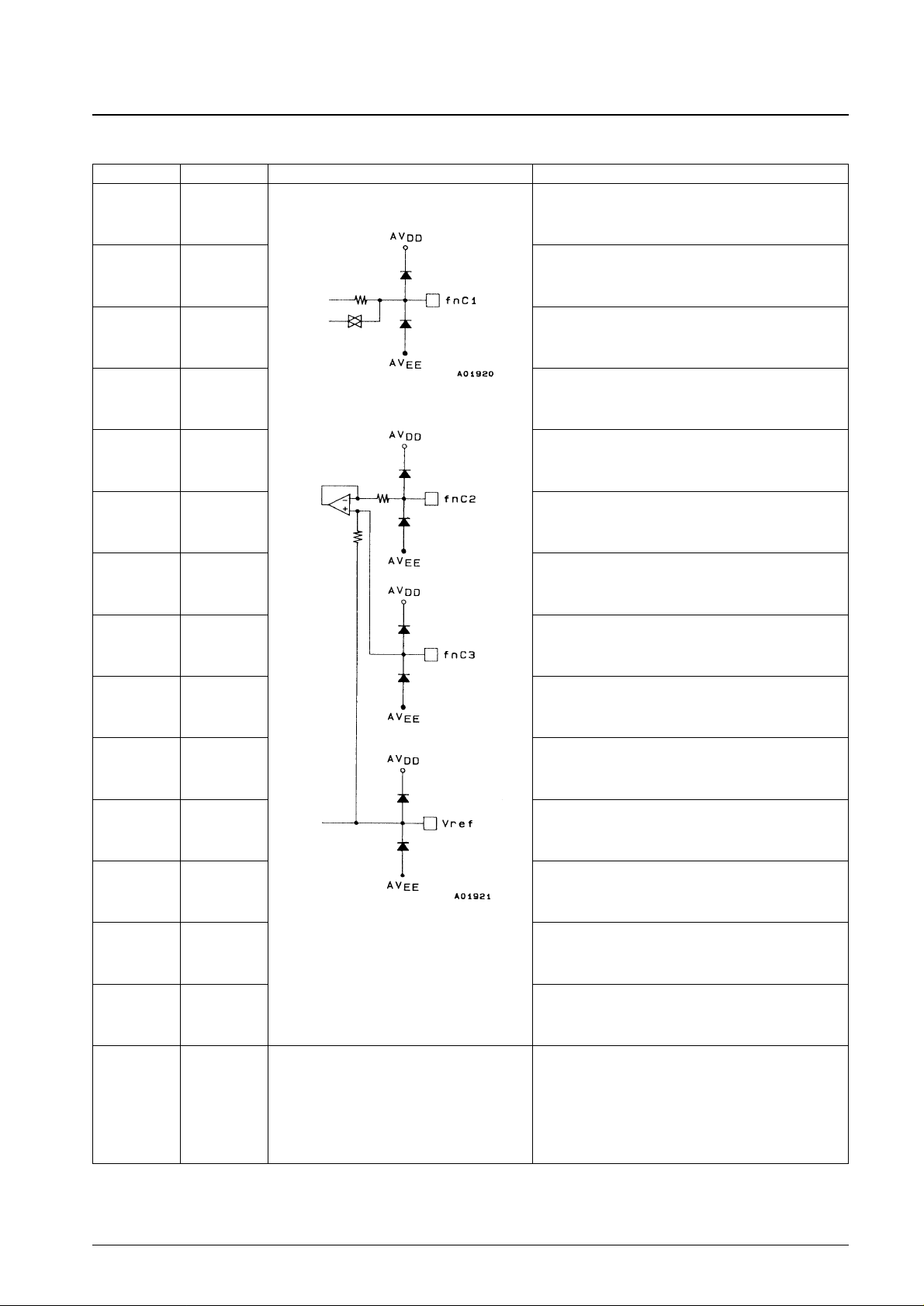
Equivalent Circuit
Internal Equivalent Circuit (for a single band)
No. 4466-6/11
LC7527E
Page 7

Data Input
The LC7527E is controlled by inputting stipulated data using the CE, CL, and DI pins. The data has a total of 20 bits, of
which eight are address and 12 are data.
No. 4466-7/11
LC7527E
Page 8

Sample Application Circuit
Note: If at all possible, use bipolar capacitors for all capacitors that do not have a polarity specified.
*1. A resistor of about 100 kΩis recommended if impulse noise (popping sounds) is a problem.
Unit (resistance: Ω, capacitance: F)
No. 4466-8/11
LC7527E
Page 9

External Component Value Calculations
The external capacitors required for each band in the LC7527E are the structural elements in semiconductor inductors
(simulated inductors). The remainder of this section presents the equivalent circuits and the formulas used to determine
the center frequencies.
1. Semiconductor Inductor Equivalent Circuit
The LC7527E provides circuits with differing constants for the low and high bands.
2. Calculation Example
Specifications: 1) Center frequency: Fo = 63 Hz
2) Q at maximum boost: Q
+12 dB
= 1.05
• Derive the sharpness Qo of the semiconductor inductor itself.
Qo = × Q
+12 dB
≈ 4.064 See the internal equivalent circuit figure for R4.
• Derive C1.
C1 = 1/2πFoR1Qo ≠ 0.953 (µF)
• Derive C2.
C2 = Qo/2πFoR2 ≠ 0.034 (µF)
3. Sample Values for C1 and C2
(R1 + R4)
R1
No. 4466-9/11
LC7527E
Center
C1 C2
frequency
(F) (F)
Fo (Hz)
63 0.953 µ 0.034 µ
160 0.377 µ 0.014 µ
400 0.151 µ 5390 p
1000 0.060 µ 2156 p
2500 0.024 µ 862 p
6300 9563 p 3422 p
16000 3765 p 1348 p
Page 10

No. 4466-10/11
LC7527E
Page 11

No. 4466-11/11
LC7527E
Usage Notes
1. The states of the internal analog switches are undefined when power is first applied. System output should be muted
until control data has been sent to the LC7527E.
2. To prevent the high frequency digital signals associated with data transfers over the CL, CI, and DI pins from
generating interference in the analog signals, either guard those lines with a ground pattern or use shielded cables.
This catalog provides information as of October, 1996. Specifications and information herein are subject to
change without notice.
■ No products described or contained herein are intended for use in surgical implants, life-support systems, aerospace
equipment, nuclear power control systems, vehicles, disaster/crime-prevention equipment and the like, the failure of
which may directly or indirectly cause injury, death or property loss.
■ Anyone purchasing any products described or contained herein for an above-mentioned use shall:
➀ Accept full responsibility and indemnify and defend SANYO ELECTRIC CO., LTD., its affiliates, subsidiaries and
distributors and all their officers and employees, jointly and severally, against any and all claims and litigation and all
damages, cost and expenses associated with such use:
➁ Not impose any responsibility for any fault or negligence which may be cited in any such claim or litigation on
SANYO ELECTRIC CO., LTD., its affiliates, subsidiaries and distributors or any of their officers and employees
jointly or severally.
■ Information (including circuit diagrams and circuit parameters) herein is for example only; it is not guaranteed for
volume production. SANYO believes information herein is accurate and reliable, but no guarantees are made or implied
regarding its use or any infringements of intellectual property rights or other rights of third parties.
 Loading...