

Page 1
Ordering number : EN*5965
40299RM (OT) No. 5965-1/25
Overview
The LC74792/JM is a CMOS IC that provides PDC, VPS,
and UDT data acquisition functions. The LC74792/JM
supports microprocessor control of its operating modes
and microprocessor read out of data acquired in any of its
operating modes.
Features
• VPS data acquisition (5 or 11 to 15 bytes)
VPS: Video Program System
• PDC (8/30/2) data acquisition (13 to 25 bytes)
PDC: Program Delivery Control
• UDT (8/30/1) data acquisition (13 to 25 bytes)
UDT: Unified Date and Time
• Header (X/00) data acquisition (14 to 45 bytes)
• Status display (8/30/1, 8/30/2) data acquisition (26 to
45 bytes)
• Automatic VPS/PDC discrimination mode
• Built-in AFC and sync separator circuits
• Synchronization discrimination circuit
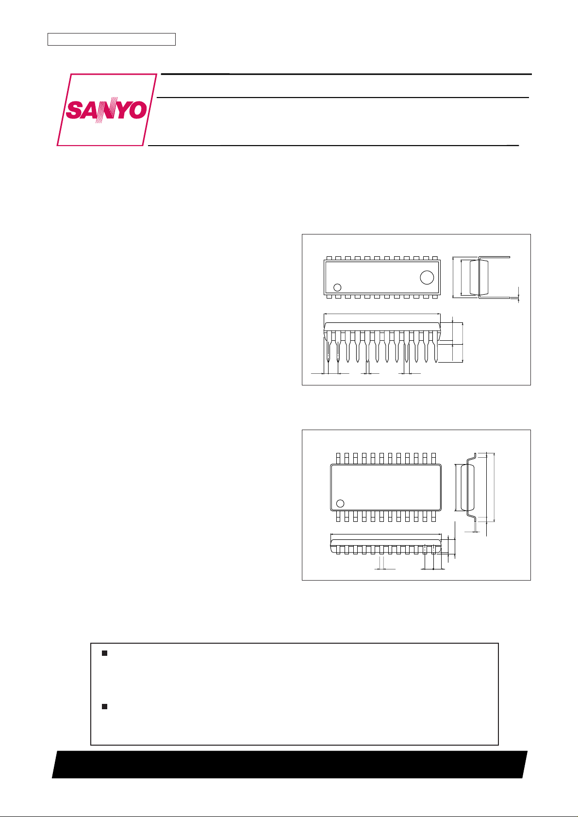
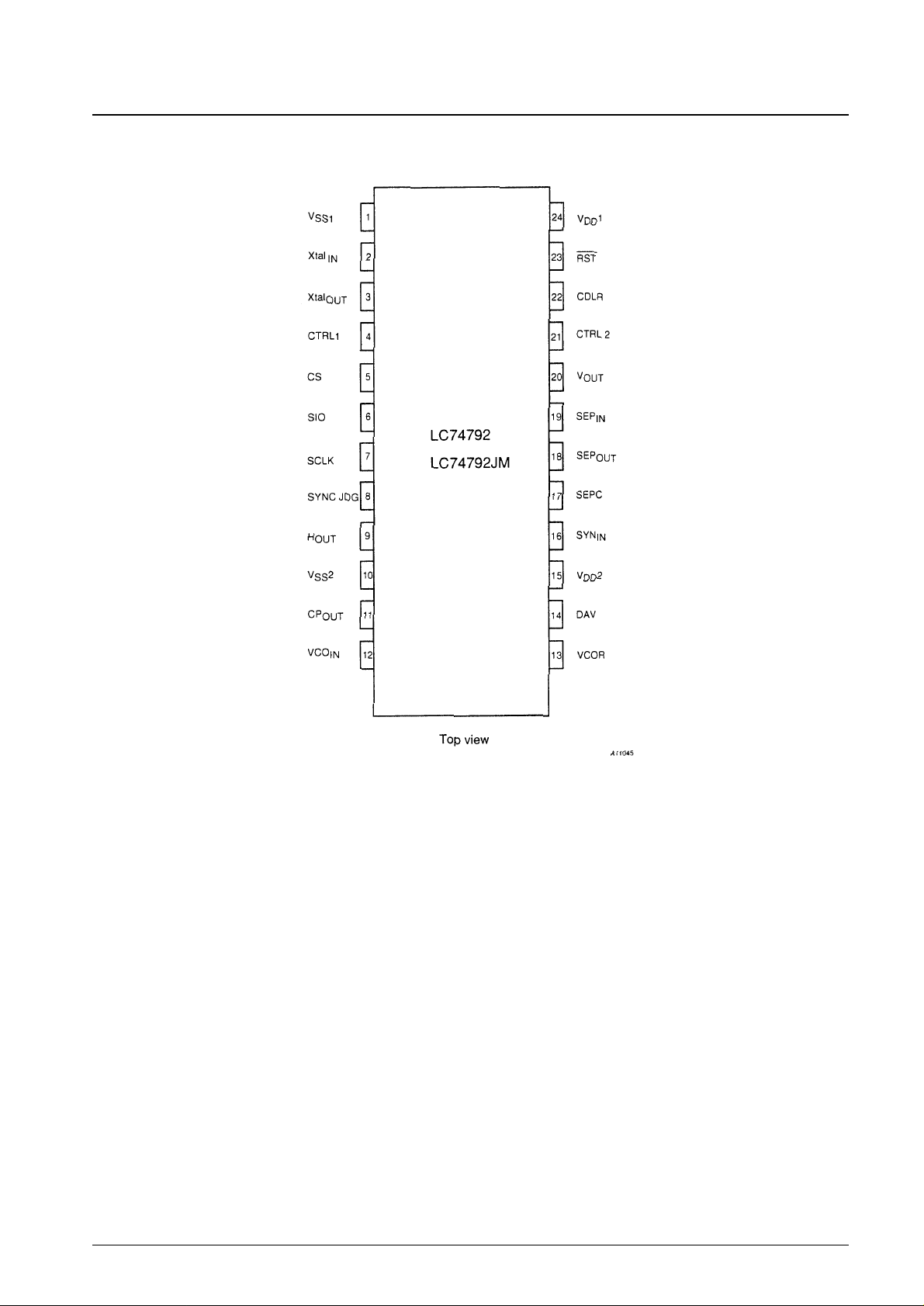
Package Dimensions
unit: mm
3067-DIP24S
unit: mm
3112-MFP24S
0.48
3.25
3.3
3.9max
0.51min
21.2
0.81 1.78
0.25
7.62
6.4
1
12
24
13
0.95
Preliminary
SANYO: DIP24S
[LC74792]
112
24
13
12.6
0.8
1.0
0.15
0.35
5.4
6.35
7.6
0.625
1.8max
1.5
0.1
SANYO: MFP24S
[LC74792JM]
LC74792, 74792JM
SANYO Electric Co.,Ltd. Semiconductor Company
TOKYO OFFICE Tokyo Bldg., 1-10, 1 Chome, Ueno, Taito-ku, TOKYO, 110-8534 JAPAN
VPS / PDC Slicer IC
CMOS IC
Any and all SANYO products described or contained herein do not have specifications that can handle
applications that require extremely high levels of reliability, such as life-support systems, aircraft’s
control systems, or other applications whose failure can be reasonably expected to result in serious
physical and/or material damage. Consult with your SANYO representative nearest you before using
any SANYO products described or contained herein in such applications.
SANYO assumes no responsibility for equipment failures that result from using products at values that
exceed, even momentarily, rated values (such as maximum ratings, operating condition ranges, or other
parameters) listed in products specifications of any and all SANYO products described or contained
herein.
Page 2
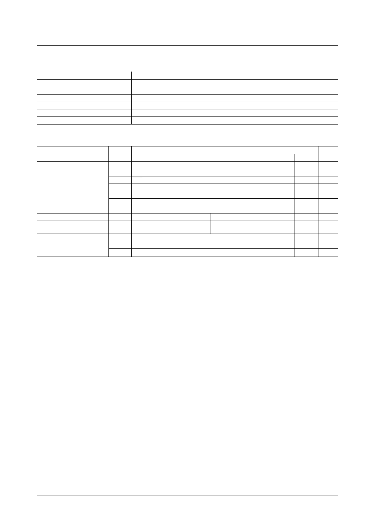
Pin Assignment
No. 5965-2/25
LC74792, 74792JM
Page 3

No. 5965-3/25
LC74792, 74792JM
Pin Functions
Pin No. Pin Function Description
1 V
SS
1 Ground Digital system ground
2 Xtal
IN
Crystal oscillator connections
Connections for the crystal element and capacitors that form the crystal oscillator. Also
3 Xtal
OUT
used for external clock input (fsc, 2fsc, or 4fsc).
4 CTRL1 Crystal element switching
Switches between external clock input mode and crystal oscillator mode. Set this pin low
for crystal oscillator, and high for external clock input.
5 CS Enable input pin Enable input pin (hysteresis input)
6 SIO Data input/output pin Data input/output pin (hysteresis input)
7 SCLK Clock input pin Clock input pin (hysteresis input)
External synchronizing signal presence/absence discrimination status output.
8 SYNC
JDG
External synchronizing signal A high level is output when synchronizing signals are present.
discrimination output This pin outputs the crystal oscillator clock when the RST pin is low.
(This reset state output can be disabled with command input.)
9 Hout Horizontal synchronizing signal output Horizontal synchronizing signal output
10 VSS2 Ground Ground. (VCO circuit ground)
11 CP
OUT
Charge pump output Charge pump output. Connect a low-pass filter to this pin.
12 VCO
IN
Oscillator control voltage input VCO oscillation control voltage input
13 VCOR Oscillator range adjustment VCO oscillation range adjustment resistor connection
14 DAV Data acquisition output Outputs a low level when PDC/VPS data has been discriminated
15 V
DD
2 Power supply (+5 V) Power supply (+5 V) (VCO system power supply)
16 SYN
IN
Sync separator circuit input Internal sync separator circuit video signal input
17 SEPC Slice level output Slice level verification
18 SEP
OUT
Composite synchronizing signal output Internal sync separator circuit composite synchronizing signal output
Inputs the vertical synchronizing signal by integrating the SEP
OUT
pin output signal.
19 SEP
IN
Vertical synchronizing signal input Applications must connect the SEP
OUT
pin to this pin through an integration circuit. If
unused, connect this pin to VDD1. (This pin is enabled when CTRL2 is high.)
Vertical synchronizing signal output
20 Vout Vertical synchronizing signal output This pin outputs the VCO clock when the RST pin is low.
(This reset state output can be disabled with command input.)
Controls whether or not the VSYNC vertical synchronizing signal is input to the SEP
IN
21 CTRL2 SEPINinput control
input.
When low: The VSYNC signal is not input. (The internal vertical separation circuit is used.)
When high: The VSYNC signal is input.
22 CDLR Clock phase adjustment Connection for the clock phase adjustment resistor
23 RST Reset input
System reset input.
A pull-up resistor is built in. (This input has hysteresis characteristics.)
24 V
DD
1 Power supply (+5 V) Power supply. (+5 V: digital system power supply)
Page 4
No. 5965-4/25
LC74792, 74792JM
Parameter Symbol Conditions Ratings Unit
Supply voltage V
DD
max VDD1 and VDD2 VSS– 0.3 to VSS+ 7.0 V
Input voltage V
IN
All input pins VSS– 0.3 to VDD1 + 0.3 V
Output voltage V
OUT
SIO, SYNCJDG, SEPOUT, DAV, HOUT, and VOUT VSS– 0.3 to VDD1 + 0.3 V
Allowable power dissipation Pd max Ta = 25°C 350 mW
Operating temperature Topr –30 to +70 °C
Storage temperature Tstg –40 to +125 °C
Specifications
Absolute Maximum Ratings
Parameter Symbol Conditions
Ratings
Unit
min typ max
Supply voltage V
DD
1 VDD1 and VDD2 4.5 5.0 5.5 V
V
IH
1 CS, SIO and SCLK 0.8 VDD1 5.5 V
High-level input voltage V
IH
2 RST 0.8 VDD1 VDD1 + 0.3 V
V
IH
3 CTRL1 and CTRL2 0.7 VDD1 VDD1 + 0.3 V
Low-level input voltage
V
IL
1 RST, CS, SIO and SCLK VSS– 0.3 0.2 VDD1 V
V
IL
2 CTRL1 and CTRL2 VSS– 0.3 0.3 VDD1 V
Pull-up resistance R
PU
RST 25 50 90 kΩ
Composite video signal input voltage
VIN1 SYN
IN
VDD1 = 5 V 1.5 2.0 2.5 Vp-p
Input voltage V
IN
2
Xtal
IN
(in external clock input mode)
V
DD
1 = 5 V 0.10 5.0 Vp-p
fin = fsc, 2fsc, or 4fsc
F
OSC
1 The XtalINand Xtal
OUT
oscillator pins (4fsc: PAL) 17.734 MHz
Oscillator frequency F
OSC
2 The XtalINand Xtal
OUT
oscillator pins (2fsc: PAL) 8.867 MHz
F
OSC
3 The XtalINand Xtal
OUT
oscillator pins (fsc: PAL) 4.433 MHz
Recommended Operating Conditions
Note that adequate measure must be taken to prevent noise from entering the XtalINpin when it is used in clock input mode.
Page 5
No. 5965-5/25
LC74792, 74792JM
Parameter Symbol Applicable pins Conditions
Ratings
Unit
min typ max
Output off leakage current Ileak2 DAV and SIO 1 µA
High-level output voltage VOH1
SEPOUT, CPOUT, SYNCJDG, V
DD
1 = 4.5 V,
3.5 V
HOUT, and VOUT I
OH
= –1.0 mA
V
OL
1
SEPOUT, CPOUT, SYNCJDG, V
DD
1 = 4.5 V
1.0 V
Low-level output voltage
DAV, HOUT, and VOUT I
OL
= 1.0 mA
V
OL
2 SIO
V
DD
1 = 5.0 V
0.4 V
I
OL
= 3.0 mA
I
IH
RST, SIO, SCLK, CTRL1, CTRL2,
V
IN
= VDD1 1 µA
Input current
VCOIN
I
IL
SIO, SCLK, CTRL1, CTRL2,
V
IN
= VSS1 –1 µA
VCOIN
With all outputs open
Operating current drain I
DD
1 VDD1 and VDD2 and a 17.734 MHz 40 mA
crystal
Electrical Characteristics at Ta = –30 to +70°C, VDD1 = 5 V unless otherwise specified.
Parameter Symbol Conditions
Ratings
Unit
min typ max
Minimum input pulse width
tw (sclk) SCLK 200 ns
tw (cs) CS pin (while CS = "H") 1 µs
Data setup time
tsu (cs) CS 200 ns
tsu (sin) SIN 200 ns
Data setup time
th (cs) CS 2 µs
th (sin) SIN 200 ns
1-word write time
tword 8-bit data write time 4.2 µs
twt RAM data write time 1 µs
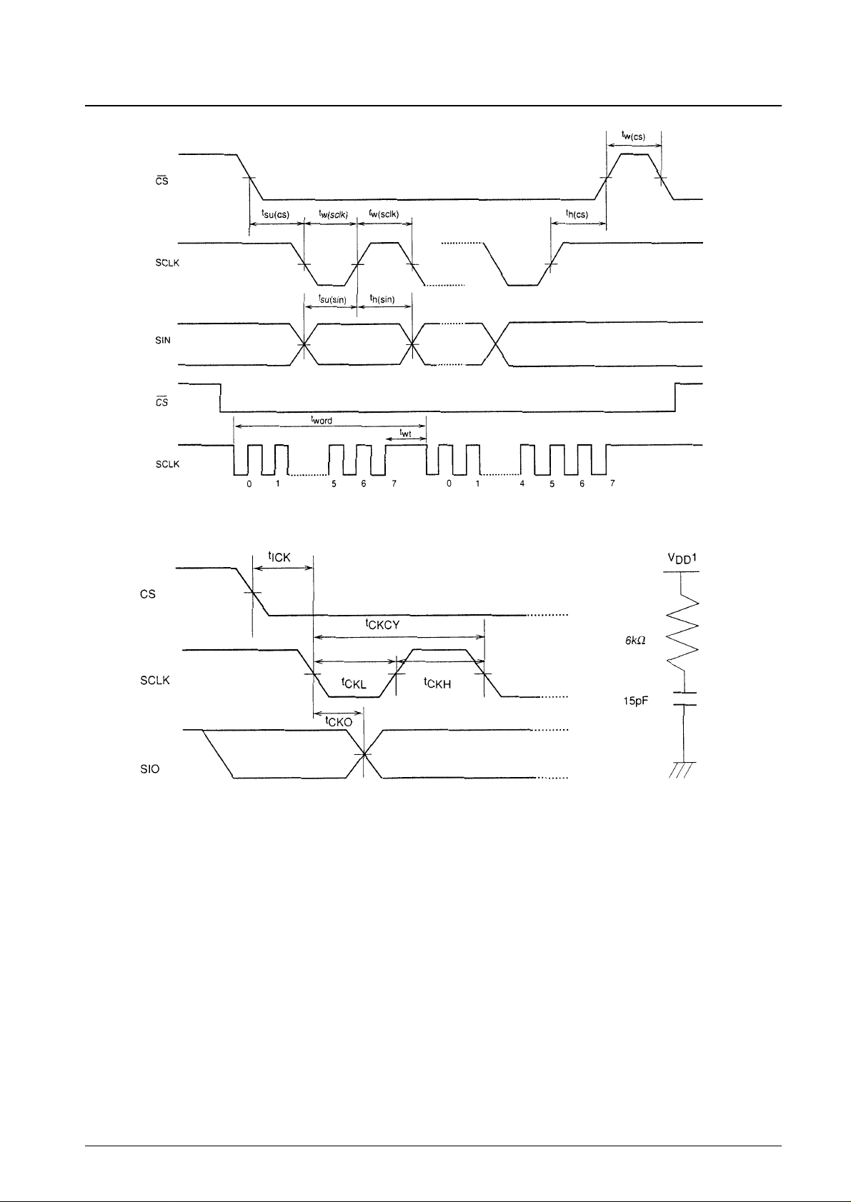
Timing Characteristics
[Write] (Refer to Figure 1) at Ta = –30 to +70°C, VDD1 = 5±0.5 V
Parameter Symbol Conditions
Ratings
Unit
min typ max
t
CKCY
SCLK 2 µs
Minimum input pulse width t
CKL
SCLK 1 µs
t
CKH
SCLK 1 µs
Data setup time t
ICK
SCLK 10 µs
Output delay time t
CKO
SIO 0.5 µs
[Read] (Refer to Figure 2) (in case of N-ch open-drain type) at Ta = –30 to +70°C, VDD1 = 5±0.5 V
Note: In case of CMOS output type, depends on OSD timing.
Page 6
No. 5965-6/25
LC74792, 74792JM
Figure 1 Serial Data Input Timing
(Test load)
Figure 2 Serial Data Input Timing (in case of N-ch open-drain type)
Page 7
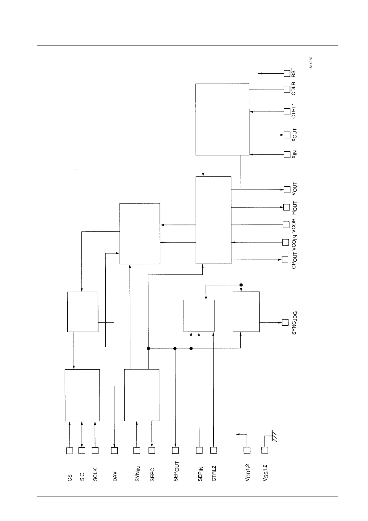
System Block Diagram
No. 5965-7/25
LC74792, 74792JM
Sync separator and data
separator circuit
Synchronization
recognition circuit
Vertical
separator
circuit
Timing generator
AFC circuit (VCO)
Data acquisition circuit
Data latch
circuit
Interface
Page 8
Control Commands
The control commands have an 8-bit serial input format. Commands consist of a command identification code in the first
byte and data in the following bytes.
Command 00: Data read mode set command
Command 0: Clock control command
Command 1: VPS/PDC control command 1
Command 2: VPS/PDC control command 2
Command 3: Synchronizing signal detection command 1
Command 4: Synchronizing signal detection command 2
Command 5: Output control command 1
Command 6: Output control command 2
Command 7: VPS/PDC control command 3
Command 8: VPS/PDC control command 4
Command 9: VPS/PDC control command 5
Command 10: VPS/PDC control command 6
Once written, the first byte command identification code is retained until the next first byte is written.
Data is written in second byte only continuous mode. (Automatic increment)
If COMMAND00 read mode is written, the read mode becomes fixed. The read mode is cancelled with CS "H".
No. 5965-8/25
LC74792, 74792JM
Display Control Commands: 3-wire type
First byte Second byte
Command Command ID code Data Data
7 6 5 4 3 2 1 0 7 6 5 4 3 2 1 0
COMMAND00 read mode 1 0 0 0 0 0 0 0 Data read
COMMAND0 (Clock control) 1 1 1 1 0 0 0 0 0 FS FS2 FS3 O TST O SYS
MOD RST
COMMAND1 (VPS/PDC control 1) 1 1 1 1 0 0 0 1 0 CPA CPA CPA VPM VPM VPM VPM
2 1 0 3 2 1 0
COMMAND2 (VPS/PDC control 2) 1 1 1 1 0 0 1 0 0 VMW VMW HBS HBS BMS EMS DCE
SE2 SEL 2 1
COMMAND3
(Synchronizing signal detection 1)
1 1 1 1 0 0 1 1 0 RN RN RN SN SN SN SN
2 1 0 3 2 1 0
COMMAND4
(Synchronizing signal detection 2)
1 1 1 1 0 1 0 0 0 0 RNE SJN SJN SJN SJC SJC
0 3 2 1 1 0
COMMAND5 (Output control 1) 1 1 1 1 0 1 0 1 0 SP0 SP0 SP0 SJ0 SJ0 VNP VSP
2 1 0 1 0 SEL SEL
COMMAND6 (Output control 2) 1 1 1 1 0 1 1 0 0 0 NP1 NP0 VI0 HI0 V0T H0T
SET SET KST KST
COMMAND7 (VPS/PDC control 3) 1 1 1 1 0 1 1 1 0 0 ECV ECV ECV ECV ECV ECV
15 14 13 12 11 5
COMMAND8 (VPS/PDC control 4) 1 1 1 1 1 0 0 0 0 ECP ECP ECP ECP ECP ECP ECP
19 18 17 16 15 14 13
COMMAND9 (VPS/PDC control 5) 1 1 1 1 1 0 0 1 0 0 ECP ECP ECP ECP ECP ECP
25 24 23 22 21 20
COMMAND10 (VPS/PDC control 6) 1 1 1 1 1 0 1 0 0 HXA LKA MSK KMW SLH SLH SLH
LL2 SLC H1 3 2 1
Page 9

No. 5965-9/25
LC74792, 74792JM
Command 0 (Clock Settings Command)
• First byte
DA 0 to 7 Register
Contents
Notes
Status Function
7 — 1 First byte identification bit
6 — 1 Command 0 identification code.
5 — 1 Clock settings.
4 — 1
3 — 0
2 — 0
1 — 0
0 — 0
• Second byte
Setting for the frequency input to the
Xtal
IN
pin (pin 2).
CDLR can be deleted: The resistor
connected to the CDLR pin may be
removed.
DA 0 to 7 Register
Contents
Notes
Status Function
7 — 0 Second byte identification bit
6 FS
0
1
5 FS2
0
1
4 FS3
0
1
3 — 0
2 TSTMOD
0 Normal operating mode
This bit must be set to 0.
1 Test mode
1 — 0
0 SYSRST
0
1 All registers are reset
FS FS2 FS3 Setting
0 0 0 2FSC
1 0 0 4FSC (CDLR can be deleted)
0 1 1 FSC
0 0 1 2FSC (CDLR can be deleted)
Command 00 (Data read mode set command)
• First byte
DA 0 to 7 Register
Contents
Notes
Status Function
7 — 1 First byte identification bit
6 — 0 Command 00 identification code.
5 — 0 Clock settings.
4 — 0
3 — 0
2 — 0
1 — 0
0 — 0
• Second byte
DA 0 to 7 Register
Contents
Notes
Status Function
7 — — Data read out
6 — —
5 — —
4 — —
3 — —
2 — —
1 — —
0 — —
Page 10

No. 5965-10/25
LC74792, 74792JM
Command 1 (VPS/PDC control command 1)
• First byte
DA 0 to 7 Register
Contents
Notes
Status Function
7 — 1 First byte identification bit
6 — 1 Command 1 identification code.
5 — 1 VPS/PDC control settings 1.
4 — 1
3 — 0
2 — 0
1 — 0
0 — 1
• Second byte
Data acquisition clock selection.
The clock can be shifted relative to
the data in units of 8 clock cycles.
DA 0 to 7 Register
Contents
Notes
Status Function
7 — 0 Second byte identification bit
6 CPA2
0
1
5 CPA1
0
1
4 CPA0
0
1
3 VPM3
0
1
2 VPM2
0
1
Slicer operating mode selection
1 VPM1
0
1
0 VPM0
0
1
CPA2 CPA1 CPA0 Clock
0 0 0 NO1
0 0 1 NO2
0 1 0 NO3
0 1 1 NO4
1 0 0 NO5
1 0 1 NO6
1 1 0 NO7
1 1 1 NO8
M3 M2 M1 MO Operating mode
0 0 0 0 VPS
0 0 0 1 8/30/2 (PDC)
0 0 1 0 PDC and VPS automatic recognition 1
0 0 1 1 8/30/1 (UDT)
0 1 0 0 Header time 1
0 1 0 1 Header time 2
0 1 1 0 Header time 3
0 1 1 1 Header time 4
1 0 0 0 Status display 1
1 0 0 1 Status display 2
1 0 1 0 Status display 3
1 0 1 1 Status display 4
1 1 0 0 PAL PULSE
1 1 0 1 PDC and VPS automatic recognition 2
1 1 1 0 PDC and VPS automatic recognition 3
1 1 1 1 PDC and VPS automatic recognition 4
Note: All registers are cleared to 0 when the IC is reset by the RST pin.
Page 11

No. 5965-11/25
LC74792, 74792JM
Command 2 (VPS/PDC control command 2)
• First byte
DA 0 to 7 Register
Contents
Notes
Status Function
7 — 1 First byte identification bit
6 — 1 Command 2 identification code.
5 — 1 VPS/PDC control settings 2.
4 — 1
3 — 0
2 — 0
1 — 1
0 — 0
• Second byte
DA 0 to 7 Register
Contents
Notes
Status Function
7 — 0 Second byte identification bit
6 VMWSE2
0 From the vertical mask period start return period
CPOUT pin (pin 11) vertical mask
1 From 10H before the vertical mask period start return period
period switching 2
5 VMWSEL
0 The vertical mask period is the return period
CPOUT pin (pin 11) vertical mask
1 The vertical mask period is 9H
period switching
4 HBS2
0 Clock run discrimination 1 (2 times)
Clock run discrimination circuit setting
1 Clock run discrimination 2 (4 times)
3 HBS1
0 Framing code discrimination 1
Framing code discrimination selection
1 Framing code discrimination 2 (A single bad bit is ignored)
0
Error check enabled (The error check can be turned on or off on
2 BMS
per-byte basis.)
1
Error check disabled (Applications can select whether data with errors
is held or written for each byte.)
1 EMS
0 Data hold
1 Data write (Error bits are set to 0 in VPS mode)
Error check turned on for unused bytes
0
VPS: bytes 3, 4, and 6 to 10, PDC: bytes 7 to 12
Header 1: bytes 14 to 37, 2: 14 to 29, 3 14 to 21.
0 DCE
Status 1 (3): bytes 7 to 25, status 2 (4) bytes 7 to 35.
Error check turned off for unused bytes
1
VPS: bytes 3, 4, and 6 to 10, PDC: bytes 7 to 12
Header 1: bytes 14 to 37, 2: 14 to 29, 3 14 to 21.
Status 1 (3): bytes 7 to 25, status 2 (4) bytes 7 to 35.
When set to 0: If there are no errors in bytes
for which the error check is turned on, those
bytes will be written to P-S (COM7-9).
When set to 1: Data is written to P-S
regardless of whether or not errors occurred.
When error checking is enabled, specifies the
processing when an error occurs in a byte for
which error checking was turned off
Error check setting for unused data
bytes
Biphase (VPS),
Hamming (PDC),
Odd parity (header)
Note: All registers are cleared to 0 when the IC is reset by the RST pin.
Page 12

No. 5965-12/25
LC74792, 74792JM
Command 3 (Synchronizing signal detection command 1)
• First byte
DA 0 to 7 Register
Contents
Notes
Status Function
7 — 1 First byte identification bit
6 — 1 Command 3 identification code.
5 — 1 Synchronizing signal detection settings 1.
4 — 1
3 — 0
2 — 0
1 — 1
0 — 1
• Second byte
DA 0 to 7 Register
Contents
Notes
Status Function
7 — 0 Second byte identification bit
6 RN2
0
1
5 RN1
0
1
4 RN0
0
1
3 SN3
0
1
2 SN2
0
1
1 SN1
0
1
0 SN0
0
1
RN2 RN1 RN0 Number of HSYNC detections
0 0 0 0 (32)
0 0 1 4 (64)
0 1 0 8 (128)
1 0 0 16 (256)
External synchronizing signal detection
control.
Signal absent
→
present discrimination.
Sets the sampling period during which SYNC
is continuously detected in the horizontal
synchronizing signal period (1H).
Values in parentheses apply when RNE0
(COM4) is set to 1.
External synchronizing signal
detection control.
Signal present → absent
discrimination.
Sets the sampling period during which
SYNC cannot be detected
consecutively in the horizontal
synchronizing signal period (1H).
SN3 SN2 SN1 SNO Number of HSYNC detections
0 0 0 0 No detection performed
0 0 0 1 32
0 0 1 0 64
0 1 0 0 128
1 0 0 0 256
Note: All registers are cleared to 0 when the IC is reset by the RST pin.
Page 13

No. 5965-13/25
LC74792, 74792JM
Command 4 (Synchronizing signal detection command 2)
• First byte
DA 0 to 7 Register
Contents
Notes
Status Function
7 — 1 First byte identification bit
6 — 1 Command 4 identification code.
5 — 1 Synchronizing signal detection settings 2.
4 — 1
3 — 0
2 — 1
1 — 0
0 — 0
• Second byte
DA 0 to 7 Register
Contents
Notes
Status Function
7 — 0 Second byte identification bit
6 — 0
5 RNE0
0 Synchronization signal discrimination absent → preset: Normal values
1
Synchronization signal discrimination absent →preset: Values in parentheses
4 SJNS3
0
1
3 SJNS2
0
1
2 SJNS1
0
1
1 SJCS1
0
1
0 SJCS0
0
1
SJNS3 SJNS2 SJNS1 Count
0 0 0 None
0 0 1 4
0 1 0 8
0 1 1 16
1 0 0 32
1 0 1 64
1 1 0 128
1 1 1 256
SJCS1 SJCS0 PAL NTSC
0 0 677 ns (1/3) 558 ns (1/2)
0 1 903 ns (1/4) 838 ns (1/3)
1 0 450 ns (1/2) 1117 ns (1/4)
Changes the values used for
synchronizing signal discrimination in
the absent → preset direction (COM3).
Setting for the noise exclusion circuit
used for synchronizing signal
discrimination in the absent → preset
direction.
If the number of H signal inputs during
a 1H period is greater than or equal to
the value listed in the table, the IC
determines that the signal is absent.
Synchronization discrimination.
HSYNI signal switching clock
selection.
Note: All registers are cleared to 0 when the IC is reset by the RST pin.
Page 14

No. 5965-14/25
LC74792, 74792JM
Command 5 (Output control command 1)
• First byte
DA 0 to 7 Register
Contents
Notes
Status Function
7 — 1 First byte identification bit
6 — 1 Command 5 identification code.
5 — 1 Output control settings 1
4 — 1
3 — 0
2 — 1
1 — 0
0 — 1
• Second byte
DA 0 to 7 Register
Contents
Notes
Status Function
7 — 0 Second byte identification bit
6 SPO2
0
1
5 SPO1
0
1
4 SPO0
0
1
3 SJO1
0
1
2 SJO0
0
1
1 VNPSEL
0 Vertical signal falling edge detection
1 Vertical signal rising edge detection
0 VSPSEL
0 VSEP: About 8.9 µs (NTSC)
1 VSEP: About 17.8 µs (NTSC)
SPO2 SPO1 SPO0 SEPout pin
0 0 0 CSYNC
0 0 1 Slice data amplitude
0 1 0 O/E
0 1 1 CLK (acquisition)
1 0 0 VCO 1/1
1 0 1 VCO 1/2
1 1 0 VCO 1/3
1 1 1 VCO 1/4
SJO1 SJO0 SYNC
JDG
pin
0 0 SYNC
JDG
0 1 LOCK
1 0 SYNCdet
1 1 DXout (Sliced data)
SEPOUT (pin 18) output switching
SYNCJDG (pin 8) output switching
Vertical signal acquisition polarity switching.
Only valid when internal vertical separation
used.
Internal vertical separation time switching
Note: All registers are cleared to 0 when the IC is reset by the RST pin.
Page 15

No. 5965-15/25
LC74792, 74792JM
Command 6 (Output control command 2)
• First byte
DA 0 to 7 Register
Contents
Notes
Status Function
7 — 1 First byte identification bit
6 — 1 Command 6 identification code.
5 — 1 Output control settings 2.
4 — 1
3 — 0
2 — 1
1 — 1
0 — 0
• Second byte
DA 0 to 7 Register
Contents
Notes
Status Function
7 — 0 Second byte identification bit
6 — 0
5 NP1
0 PAL
1 NTSC
4 NP0
0 625
Number of scan lines
1 525
3 VIOSET
0 VSYNC signal output
VOUT mode setting
1 Set up as a general-purpose port
2 HIOSET
0 HSYNC signal output
HOUT mode setting
1 Set up as a general-purpose port
1 VOTKST
0 Negative polarity (Lo)
1 Positive polarity (Hi)
0 HOTKST
0 Negative polarity (Lo)
1 Positive polarity (Hi)
VOUT polarity selection.
Level in parentheses applies when set
up as a general-purpose port.
HOUT polarity selection.
Level in parentheses applies when set
up as a general-purpose port.
Note: All registers are cleared to 0 when the IC is reset by the RST pin.
Page 16

No. 5965-16/25
LC74792, 74792JM
Command 7 (VPS/PDC control command 3)
• First byte
DA 0 to 7 Register
Contents
Notes
Status Function
7 — 1 First byte identification bit
6 — 1 Command 7 identification code.
5 — 1 VPS/PDC control settings 3.
4 — 1
3 — 0
2 — 1
1 — 1
0 — 1
• Second byte
DA 0 to 7 Register
Contents
Notes
Status Function
7 — 0 Second byte identification bit
6 — 0
5 ECV15
0 Byte 15 biphase error check: on (data retained)
1 Byte 15 biphase error check: off (data written)
4 ECV14
0 Byte 14 biphase error check: on (data retained)
1 Byte 14 biphase error check: off (data written)
3 ECV13
0 Byte 13 biphase error check: on (data retained)
1 Byte 13 biphase error check: off (data written)
2 ECV12
0 Byte 12 biphase error check: on (data retained)
1 Byte 12 biphase error check: off (data written)
1 ECV11
0 Byte 11 biphase error check: on (data retained)
1 Byte 11 biphase error check: off (data written)
0 ECV5
0 Byte 5 biphase error check: on (data retained)
1 Byte 5 biphase error check: off (data written)
VPS data specification when BMS is 0.
Items in parentheses are the
specification when BMS is 1.
Note: All registers are cleared to 0 when the IC is reset by the RST pin.
Page 17

No. 5965-17/25
LC74792, 74792JM
Command 8 (VPS/PDC control command 4)
• First byte
DA 0 to 7 Register
Contents
Notes
Status Function
7 — 1 First byte identification bit
6 — 1 Command 8 identification code.
5 — 1 VPS/PDC control settings 4.
4 — 1
3 — 1
2 — 0
1 — 0
0 — 0
• Second byte
DA 0 to 7 Register
Contents
Notes
Status Function
7 — 0 Second byte identification bit
0
Byte 19 Hamming error check on (Data retained)
6 ECP19
{Bytes 44, 28, 36, 20, 32, 42, 32, 42}
1
Byte 19 Hamming error check off (Data written)
{Bytes 44, 28, 36, 20, 32, 42, 32, 42}
0
Byte 18 Hamming error check on (Data retained)
5 ECP18
{Bytes 43, 27, 35, 19, 31, 41, 31, 41}
1
Byte 18 Hamming error check off (Data written)
{Bytes 43, 27, 35, 19, 31, 41, 31, 41}
0
Byte 17 Hamming error check on (Data retained)
4 ECP17
{Bytes 42, 26, 34, 18, 30, 40, 30, 40}
1
Byte 17 Hamming error check off (Data written)
{Bytes 42, 26, 34, 18, 30, 40, 30, 40}
0
Byte 16 Hamming error check on (Data retained)
3 ECP16
{Bytes 41, 25, 33, 17, 29, 39, 29, 39}
1
Byte 16 Hamming error check off (Data written)
{Bytes 41, 25, 33, 17, 29, 39, 29, 39}
0
Byte 15 Hamming error check on (Data retained)
2 ECP15
{Bytes 40, 24, 32, 16, 28, 38, 28, 38}
1
Byte 15 Hamming error check off (Data written)
{Bytes 40, 24, 32, 16, 28, 38, 28, 38}
0
Byte 14 Hamming error check on (Data retained)
1 ECP14
{Bytes 39, 23, 31, 15, 27, 37, 27, 37}
1
Byte 14 Hamming error check off (Data written)
{Bytes 39, 23, 31, 15, 27, 37, 27, 37}
0
Byte 13 Hamming error check on (Data retained)
0 ECP13
{Bytes 38, 22, 30, 14, 26, 36, 26, 36}
1
Byte 13 Hamming error check off (Data written)
{Bytes 38, 22, 30, 14, 26, 36, 26, 36}
PDC data specification when BMS is 0.
Items in parentheses are the specification when
BMS is 1.
Items in curly braces are the bytes for which the
odd parity check is turned on or off for headers
1, 2, 3, and 4, and for status 1, 2, 3, and 4.
Note: All registers are cleared to 0 when the IC is reset by the RST pin.
Page 18

No. 5965-18/25
LC74792, 74792JM
Command 9 (VPS/PDC control command 5)
• First byte
DA 0 to 7 Register
Contents
Notes
Status Function
7 — 1 First byte identification bit
6 — 1 Command 9 identification code.
5 — 1 VPS/PDC control settings 5.
4 — 1
3 — 1
2 — 0
1 — 0
0 — 1
• Second byte
DA 0 to 7 Register
Contents
Notes
Status Function
7 — 0 Second byte identification bit
6 — 0
5 ECP25
0 Byte 25 Hamming error check on (Data retained)
1 Byte 25 Hamming error check off (Data written)
4 ECP24
0 Byte 24 Hamming error check on (Data retained)
1 Byte 24 Hamming error check off (Data written)
3 ECP23
0 Byte 23 Hamming error check on (Data retained)
1 Byte 23 Hamming error check off (Data written)
0
Byte 22 Hamming error check on (Data retained)
2 ECP22
{Bytes , , , , 35, 45, 35, 45}
1
Byte 22 Hamming error check off (Data written)
{Bytes , , , , 35, 45, 35, 45}
0
Byte 21 Hamming error check on (Data retained)
1 ECP21
{Bytes , , , , 34, 44, 34, 44}
1
Byte 21 Hamming error check off (Data written)
{Bytes , , , , 34, 44, 34, 44}
0
Byte 20 Hamming error check on (Data retained)
0 ECP20
{Bytes 45, 29, 37, 21, 33, 43, 33, 43}
1
Byte 20 Hamming error check off (Data written)
{Bytes 45, 29, 37, 21, 33, 43, 33, 43}
PDC data specification when BMS is 0.
Items in parentheses are the
specification when BMS is 1.
Items in curly braces are the bytes for
which the odd parity check is turned on
or off for headers 1, 2, 3, and 4, and for
status 1, 2, 3, and 4.
Note: All registers are cleared to 0 when the IC is reset by the RST pin.
Page 19

No. 5965-19/25
LC74792, 74792JM
Command 10 (VPS/PDC control command 6)
• First byte
DA 0 to 7 Register
Contents
Notes
Status Function
7 — 1 First byte identification bit
6 — 1 Command A identification code.
5 — 1 VPS/PDC control settings 6.
4 — 1
3 — 1
2 — 0
1 — 1
0 — 0
• Second byte
DA 0 to 7 Register
Contents
Notes
Status Function
7 — 0 Second byte identification bit
6 HXALL2
0 Slice data discrimination time: Normal VPS/PDC data discrimination period
1 Discriminates the vertical return period data in all modes setting
5 LKASLC
0 Normal operation
1 Always in the locked state
4 MSKH1
0
1 AFC: A mask is applied to the horizontal signal
3 KMW
0
1 Forcibly set to high or low only during the CSYNC period
2 SLH3
0
1
1 SLH2
0
Clock discrimination method switching
1
0 SLH1
0
1
MODE S321 Clock discrimination
0 0 0 0 1 1 1 1 1 1 x x 0 0 0 0 0 0 x x
1 0 0 1 0 0 0 0 0 0 x x 1 1 1 1 1 1 x x
2 0 1 0 1 1 1 1 1 x x x 0 0 0 0 0 x x x
3 0 1 1 0 0 0 0 0 x x x 1 1 1 1 1 x x x
4 1 0 0 x x 1 1 1 1 1 1 0 0 0 0 0 0 x x
5 1 0 1 x x 0 0 0 0 0 0 1 1 1 1 1 1 x x
6 1 1 0 1 1 1 x 0 0 0 x
7 1 1 1 0 0 0 x 1 1 1 x
Note: All registers are cleared to 0 when the IC is reset by the RST pin.
Page 20

PDC/VPS Output Data Format
Data is read out in order starting with bit 7 of byte 1.
No. 5965-20/25
LC74792, 74792JM
Output data
PDC 8/30/mode
VPS mode Header time mode 1 (3) Header time mode 2 (4)
Format1 Format2
Data update bit If data has been updated, "0", not updated, "1".
Byte1 Bit7 byte15 bit0 byte16 bit0 byte11 bit0 byte38 bit0 byte22 bit0
6 1 1 1 (30) 1 (14) 1
5 2 2 2 2 2
4 3 3 3 3 3
3 4 byte17 bit0 4 4 4
2 5 1 5 5 5
1 6 2 6 6 6
0 7 3 7 7 7
Byte2 Bit7 byte16 bit0 byte18 bit0 byte12 bit0 byte39 bit0 byte23 bit0
6 1 1 1 (31) 1 (15) 1
5 2 2 2 2 2
4 3 3 3 3 3
3 4 byte19 bit0 4 4 4
2 5 1 5 5 5
1 6 2 6 6 6
0 7 3 7 7 7
Byte3 Bit7 byte17 bit0 byte20 bit0 byte13 bit0 byte40 bit0 byte24 bit0
6 1 1 1 (32) 1 (16) 1
5 2 2 2 2 2
4 3 3 3 3 3
3 4 byte21 bit0 4 4 4
2 5 1 5 5 5
1 6 2 6 6 6
0 7 3 7 7 7
Byte4 Bit7 byte18 bit0 byte22 bit0 byte14 bit0 byte41 bit0 byte25 bit0
6 1 1 1 (33) 1 (17) 1
5 2 2 2 2 2
4 3 3 3 3 3
3 4 byte23 bit0 4 4 4
2 5 1 5 5 5
1 6 2 6 6 6
0 7 3 7 7 7
Byte5 Bit7 byte19 bit0 byte14 bit0 byte5 bit0 byte42 bit0 byte26 bit0
6 1 1 1 (34) 1 (18) 1
5 2 2 2 2 2
4 3 3 3 3 3
3 4 byte15 bit0 4 4 4
2 5 1 5 5 5
1 6 2 6 6 6
0 7 3 7 7 7
Byte6 Bit7 byte20 bit0 byte24 bit0 byte15 bit0 byte43 bit0 byte27 bit0
6 1 1 1 (35) 1 (19) 1
5 2 2 2 2 2
4 3 3 3 3 3
3 4 byte25 bit0 4 4 4
2 5 1 5 5 5
1 6 2 6 6 6
0 7 3 7 7 7
Continued on next page.
Page 21

No. 5965-21/25
LC74792, 74792JM
Continued from preceding page.
Output data
PDC 8/30/mode
VPS mode Header time mode 1 (3) Header time mode 2 (4)
Format1 Format2
Byte7 Bit7 byte21 bit0 byte13 bit0 1 byte44 bit0 byte28 bit0
6 1 1 1 (36) 1 (20) 1
5 2 2 1 2 2
4 3 3 1 3 3
3 4 1 1 4 4
2 5 1 1 5 5
1 6 1 1 6 6
0 7 1 0 7 7
Byte8 Bit7 byte13 bit0 Error byte16 Error byte11 byte45 bit0 byte29 bit0
6 1 information 1 17 information 12 (37) 1 (21) 1
5 2 18 13 2 2
4 3 19 14 3 3
3 4 20 5 4 4
2 5 21 15 5 5
1 6 22 0 6 6
0 7 23 0 7 7
Byte9 Bit7 byte14 bit0 Error byte14 Error byte38 (30) Error byte22 (14)
6 1 information 2 15 information 39 (31) information 23 (15)
5 2 24 40 (32) 24 (16)
4 3 25 41 (33) 25 (17)
3 4 13 42 (34) 26 (18)
2 5 0 43 (35) 27 (19)
1 6 0 44 (36) 28 (20)
0 7 0 45 (37) 29 (21)
Byte10 Bit7 byte22 bit0
6 1
5 2
4 3
3 4
2 5
1 6
0 7
Byte11 Bit7 byte23 bit0
6 1
5 2
4 3
3 4
2 5
1 6
0 7
Byte12 Bit7 byte24 bit0
6 1
5 2
4 3
3 4
2 5
1 6
0 7
Byte13 Bit7 byte25 bit0
6 1
5 2
4 3
3 4
2 5
1 6
0 7
Note: Data with the value 1 is output for sections for which there is no output data setting.
Page 22

No. 5965-22/25
LC74792, 74792JM
Data is read out in order starting with bit 7 of byte 1.
Status display 1 and 2: 8/30/2 Status display 1 and 2: 8/30/1
Output data
Status display mode 1 (3) Status display mode 2 (4)
PAL Puls
Data update bit If data has been updated, "0"
Byte1 Bit7 byte26 bit0 byte36 bit0 bit0
6 (26) 1 (36) 1 1
5 2 2 2
4 3 3 3
3 4 4 4
2 5 5 5
1 6 6 6
0 7 7 7
Byte2 Bit7 byte27 bit0 byte37 bit0 bit8
6 (27) 1 (37) 1 9
5 2 2 10
4 3 3 11
3 4 4 12
2 5 5 13
1 6 6 0
0 7 7 0
Byte3 Bit7 byte28 bit0 byte38 bit0
6 (28) 1 (38) 1
5 2 2
4 3 3
3 4 4
2 5 5
1 6 6
0 7 7
Byte4 Bit7 byte29 bit0 byte39 bit0
6 (29) 1 (39) 1
5 2 2
4 3 3
3 4 4
2 5 5
1 6 6
0 7 7
Byte5 Bit7 byte30 bit0 byte40 bit0
6 (30) 1 (40) 1
5 2 2
4 3 3
3 4 4
2 5 5
1 6 6
0 7 7
Byte6 Bit7 byte31 bit0 byte41 bit0
6 (31) 1 (41) 1
5 2 2
4 3 3
3 4 4
2 5 5
1 6 6
0 7 7
Continued on next page.
Note: Data with the value 1 is output for sections for which there is no output data setting.
Page 23

No. 5965-23/25
LC74792, 74792JM
Output data
Status display mode 1 (3) Status display mode 2 (4)
PAL Puls
Byte7 Bit7 byte32 bit0 byte42 bit0
6 (32) 1 (42) 1
5 2 2
4 3 3
3 4 4
2 5 5
1 6 6
0 7 7
Byte8 Bit7 byte33 bit0 byte43 bit0
6 (33) 1 (43) 1
5 2 2
4 3 3
3 4 4
2 5 5
1 6 6
0 7 7
Byte9 Bit7 byte34 bit0 byte44 bit0
6 (34) 1 (44) 1
5 2 2
4 3 3
3 4 4
2 5 5
1 6 6
0 7 7
Byte10 Bit7 byte35 bit0 byte45 bit0
6 (35) 1 (45) 1
5 2 2
4 3 3
3 4 4
2 5 5
1 6 6
0 7 7
Byte11 Bit7 Error byte26 (26) Error byte36 (36)
6 information 1 27 (27) information 1 37 (37)
5 28 (28) 38 (38)
4 29 (29) 39 (39)
3 30 (30) 40 (40)
2 31 (31) 41 (41)
1 32 (32) 42 (42)
0 33 (33) 43 (43)
Byte12 Bit7 Error byte34 (34) Error byte44 (44)
6 information 2 35 (35) information 1 45 (45)
5 0 0
4 0 0
3 0 0
2 0 0
1 0 0
0 0 0
Byte13 Bit7
6
5
4
3
2
1
0
Continued from preceding page.
Note: Data with the value 1 is output for sections for which there is no output data setting.
Page 24

Sample Application Circuit
• Using an external system clock
No. 5965-24/25
LC74792, 74792JM
Microcontroller
Page 25

PS No. 5965-25/25
LC74792, 74792JM
This catalog provides information as of April, 1999. Specifications and information herein are subject to
change without notice.
Specifications of any and all SANYO products described or contained herein stipulate the performance,
characteristics, and functions of the described products in the independent state, and are not guarantees
of the performance, characteristics, and functions of the described products as mounted in the customer’s
products or equipment. To verify symptoms and states that cannot be evaluated in an independent device,
the customer should always evaluate and test devices mounted in the customer’s products or equipment.
SANYO Electric Co., Ltd. strives to supply high-quality high-reliability products. However, any and all
semiconductor products fail with some probability. It is possible that these probabilistic failures could
give rise to accidents or events that could endanger human lives, that could give rise to smoke or fire,
or that could cause damage to other property. When designing equipment, adopt safety measures so
that these kinds of accidents or events cannot occur. Such measures include but are not limited to protective
circuits and error prevention circuits for safe design, redundant design, and structural design.
In the event that any or all SANYO products (including technical data, services) described or contained
herein are controlled under any of applicable local export control laws and regulations, such products must
not be exported without obtaining the export license from the authorities concerned in accordance with the
above law.
No part of this publication may be reproduced or transmitted in any form or by any means, electronic or
mechanical, including photocopying and recording, or any information storage or retrieval system,
or otherwise, without the prior written permission of SANYO Electric Co., Ltd.
Any and all information described or contained herein are subject to change without notice due to
product/technology improvement, etc. When designing equipment, refer to the “Delivery Specification”
for the SANYO product that you intend to use.
Information (including circuit diagrams and circuit parameters) herein is for example only; it is not
guaranteed for volume production. SANYO believes information herein is accurate and reliable, but
no guarantees are made or implied regarding its use or any infringements of intellectual property rights
or other rights of third parties.
• Using a crystal oscillator
Microcontroller
 Loading...