

Page 1
Overview
The LC74775/M is an on-screen display controller CMOS
IC that displays characters and patterns on the TV screen
under microprocessor control. This IC includes a built-in
PDC/VPS/UDT interface circuit.
Functions
• Display format: 24 characters by 12 rows (Up to 288
characters)
• Character format: 12 (horizontal) × 18 (vertical) dots
• Character sizes: Three sizes each in the horizontal and
vertical directions
• Characters in font: 128 (Of the 128 characters, one is a
space character (7E hexadecimal)
and one is a transparent space
character (7F hexadecimal))
• Initial display positions: 64 horizontal positions and 64
vertical positions
• Blinking: Specifiable in character units
• Blinking types: Two periods supported:
1.0 second and 0.5 second
• Blanking: Over the whole font (12 × 18 dots)
• Background color: 8 colors (internal synchronization
mode): 4fSCand 2f
SC
Blue background only: NTSC
• Line background color: Three lines can be set up.
8 line background colors (in
internal synchronization mode):
4fSCand 2f
SC
• External control input: 8-bit serial input format
• On-chip sync separator circuit
• Video outputs: PAL and NTSC format composite video
outputs
• On-chip PDC/VPS/UDT interface circuit supporting I2C
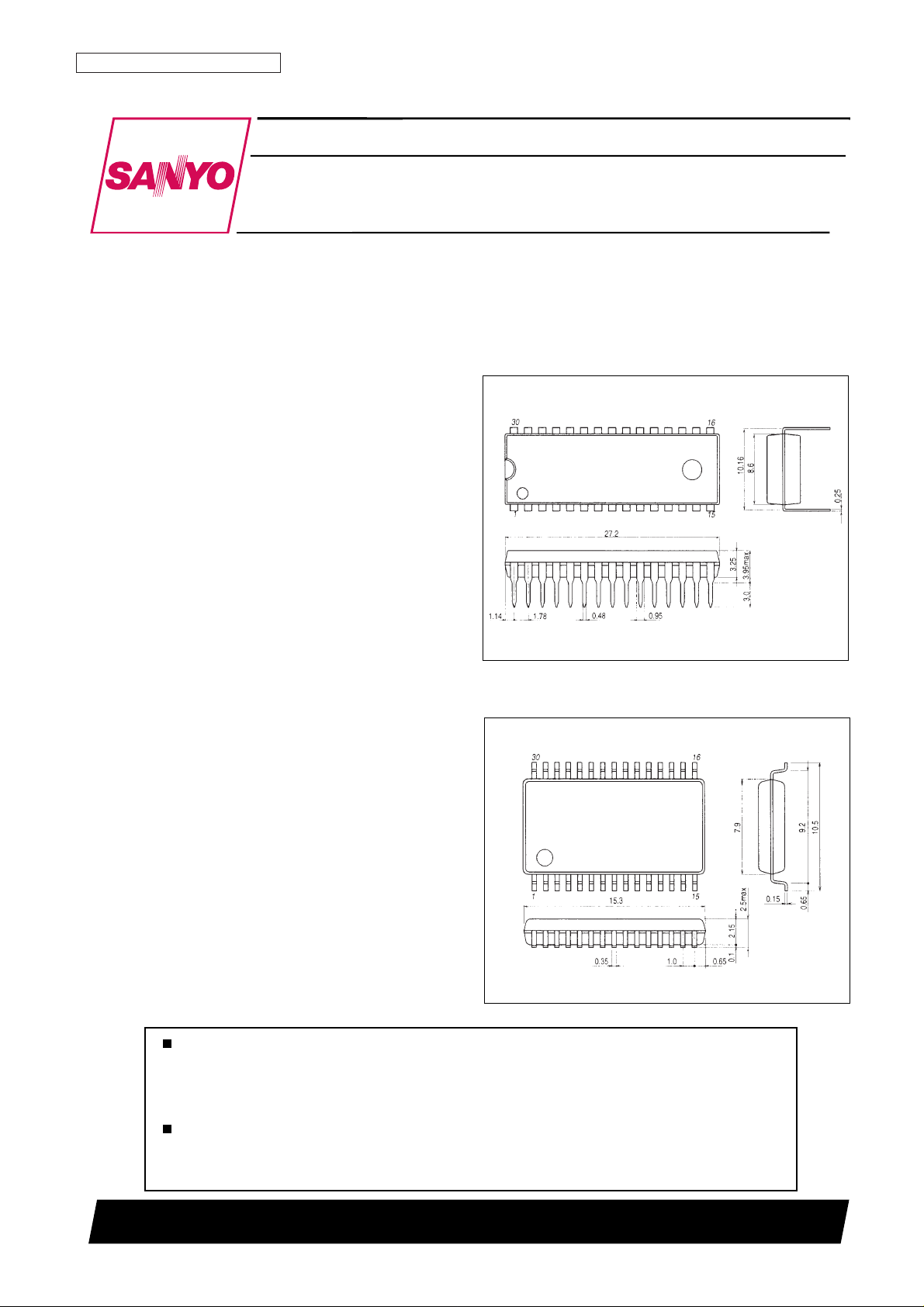
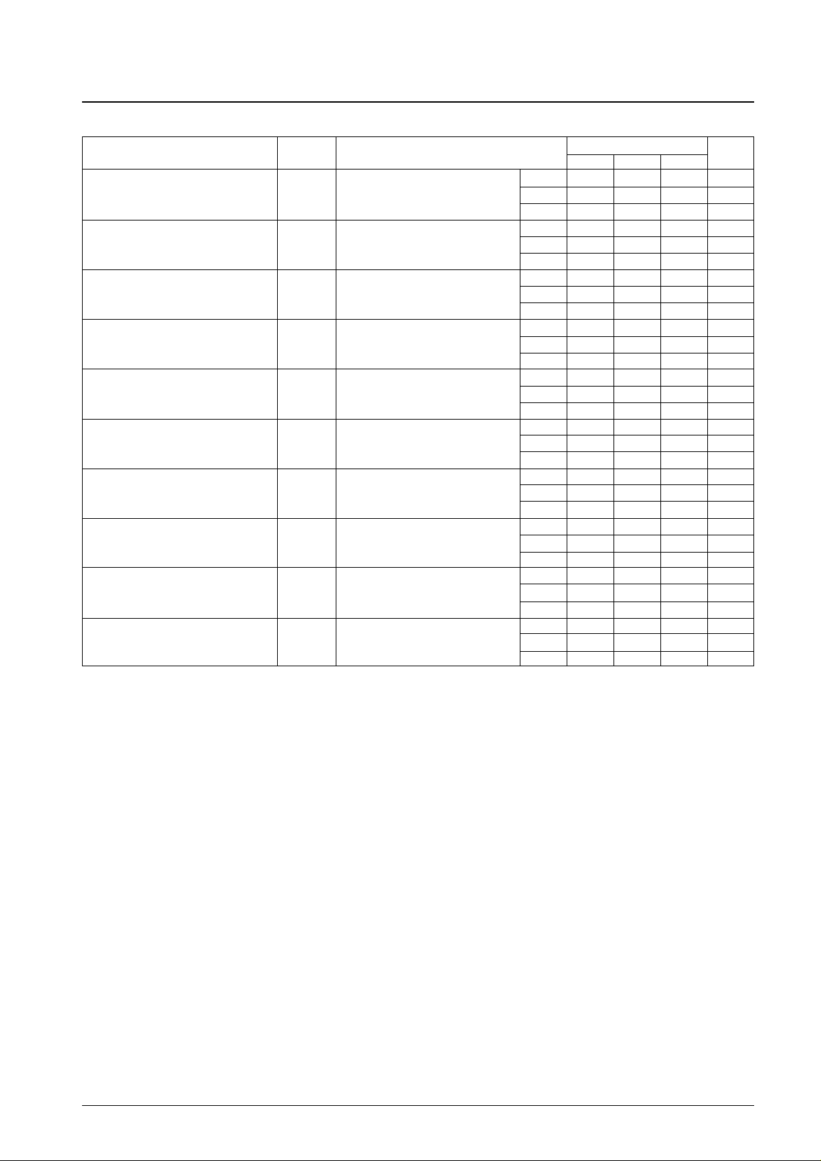
• Package: DIP30SD
MFP30S
CMOS IC
Ordering number : EN*5919
N1198RM(OT) No. 5919-1/35
Preliminary
SANYO: MFP30S
[LC74775M]
SANYO Electric Co.,Ltd. Semiconductor Bussiness Headquarters
TOKYO OFFICE Tokyo Bldg., 1-10, 1 Chome, Ueno, Taito-ku, TOKYO, 110-8534 JAPAN
On-Screen Display Controller IC
LC74775, 74775M
SANYO: DIP30SD
[LC74775]
Package Dimensions
unit: mm
3196-DIP30SD
unit: mm
3216A-MFP30S
Any and all SANYO products described or contained herein do not have specifications that can handle
applications that require extremely high levels of reliability, such as life-support systems, aircraft’s
control systems, or other applications whose failure can be reasonably expected to result in serious
physical and/or material damage. Consult with your SANYO representative nearest you before using
any SANYO products described or contained herein in such applications.
SANYO assumes no responsibility for equipment failures that result from using products at values that
exceed, even momentarily, rated values (such as maximum ratings, operating condition ranges, or other
parameters) listed in products specifications of any and all SANYO products described or contained
herein.
Page 2

Pin Assignment
No. 5919-2/35
LC74775, 74775M
Page 3

Pin Functions
No. 5919-3/35
LC74775, 74775M
Pin no. Pin Function Notes
1 V
SS
1 Ground Ground connection (digital system ground)
2 Xtal
IN
These pins are used either to connect the crystal and capacitors used to form an external
crystal oscillator circuit to generate the internal synchronizing signals, or to input an external
Xtal
OUT
Crystal oscillator
clock signal (2fsc or 4fsc). As a mask option, the Xtal
OUT
pin can be set to function as
3
(MUTE)
(MUTE input)
the MUTE input pin. When this pin is set low, the video output is held at the pedestal level.
(A pull-up resistor is built in and the input has hysteresis characteristics.)
Switches the mode between external clock input and crystal oscillator operation. A low level
4 CTRL1 selects crystal oscillator operation and a high level selects external clock input. As a mask
(CHABLK) option, the CTRL1 input pin can be set to function as the CHABLK (character . frame)
output. This is a 3-value output.
5 SCL I
2
C clock input Clock input for the PDC/VPS data output. I2C bus.
6 OSC
IN
LC oscillator
Connection for the external coil and capacitor for the oscillator used to generate
connections
the character output dot clock
7 OSC
OUT
Outputs the state of the external synchronizing signal presence/absence judgment. Outputs
External synchronizing
a high level when synchronizing signals are present.
8 SYNC
JDC
signal judgment output
Outputs either the crystal oscillator clock if CS and RST are low, or the VCO clock if CS
and RST are high.
(This signal is not output after a command reset.)
Enable input for the OSD serial data input.
9 CS Enable input Serial data input is enabled when this pin is low.
A pull-up resistor is built in and the input has hysteresis characteristics.
10 SCLK Clock input
Serial data input enable pin.
A pull-up resistor is built in and the input has hysteresis characteristics.
11 SIN Data input
Serial data input.
A pull-up resistor is built in and the input has hysteresis characteristics.
12 V
DD
2 Power supply Composite video signal level adjustment power supply (analog system power supply)
13 CP
OUT
Charge pump output Charge pump output. Connect a low-pass filter to this pin.
14 VCO
IN
Oscillator control voltage input
VCO oscillator control voltage input. (For data slicing)
15 V
SS
3 Ground Ground (VCO ground)
16 VCO
R
Oscillator range adjustment VCO oscillator range adjustment resistor connection
17 NC This pin must either be connected to ground or left open
18 V
DD
3 Power supply (+5 V) Power supply (+5 V: VCO power supply)
19 CV
OUT
Video signal output Composite video signal output
20 V
SS
2 Ground Ground (analog system ground)
21 CV
IN
Video signal input Composite video signal input
22 CV
CR
Video signal input SECAM chrominance signal input
23 V
DD
1 Power supply (+5 V) Power supply (+5 V: digital system power supply)
24 SYN
IN
Sync separator circuit input Video signal input to the internal sync separator circuit
25 SEPC Slice level output Slice level verification pin
26 SEP
OUT
Composite synchronizing Internal sync separator circuit composite synchronizing signal output. The signal actually
signal output output can be switched by MOD0 and SEL0. The DAV signal is output in the initial state.
PDC/VPS data I/O.
27 SDA I
2
C bus data I/O The I2C bus write address is [0111 1100].
The I
2
C bus read address is [0111 1101].
28 CDLR
Background color phase
Background color phase adjustment resistor connection
adjustment
29 RST Reset input
System reset input.
A pull-up resistor is built in and the input has hysteresis characteristics.
30 V
DD
1 Power supply (+5 V) Power supply (+5 V: digital system power supply)
Note: *Both VDD1 pins must be connected to power.
Crystal oscillator input
switching
(CHABLK)
Page 4

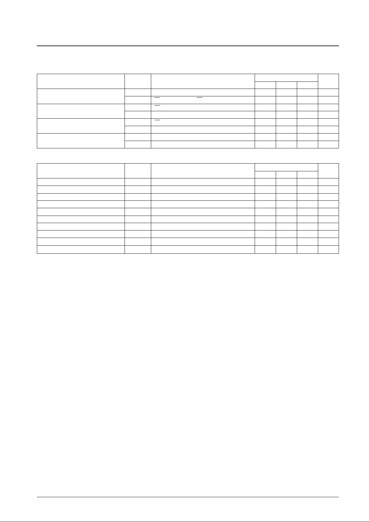
Absolute Maximum Ratings
No. 5919-4/35
LC74775, 74775M
Paremeter Symbol Conditions Ratings Unit
Maximum supply voltage V
DD
max VDD1, VDD2, and VDD3 VSS– 0.3 to VSS+ 6.5 V
Maximum input voltage V
IN
max All input pins VSS– 0.3 to VDD1 + 0.3 V
Maximum output voltage V
OUT
max SDA, SYNC
JDG
, and SEP
OUT
VSS– 0.3 to VDD1 + 0.3 V
Allowable power dissipation Pd max Ta = 25°C 350 mW
Operating temperature Topr –30 to + 70 °C
Storage temperature Tstg –40 to + 125 °C
Continued on next page.
Allowable Operating Ranges
Ratings
Paremeter Symbol Conditions
min typ max
Unit
Supply voltage
V
DD
1 VDD1, VDD3 4.5 5.0 5.5 V
V
DD
2 VDD2 4.5 5.0 6.5 V
V
IH
1 CS, SIN, SCLK, SDA, SCL, 0.8VDD1 5.5 V
Input high-level voltage V
IH
2 RST, MUTE 0.8VDD1
VDD1 + 0.3
V
V
IH
3 CTRL1 0.7VDD1
VDD1 + 0.3
V
V
IL
1
RST, CS, SIN, SCLK, SDA, SCL,
VSS– 0.3
0.2VDD1 V
Input low-level voltage
MUTE
V
IL
2 CTRL1
VSS– 0.3
0.3VDD1 V
Pull-up resistance R
PU
RST, CS, SIN, SCLK, MUTE
25 50 90 kΩ
Applies to pins set up by options.
Composite video signal
V
IN
1 CVIN, CVCR: VDD1 = 5V 2.0 Vp-p
input voltage
V
IN
2 SYNIN: VDD1 = 5V 1.5 2.0 2.5 Vp-p
Input voltage V
IN
3
Xtal
IN
(when used for external clock input)
0.10 5.0 Vp-p
f
IN
= 2fsc or 4fsc: VDD1= 5V
f
OSC
1 XtalINand Xtal
OUT
oscillator pins (2fsc: PAL) 8.867 MHz
Oscillator frequencies f
OSC
2 XtalINand Xtal
OUT
oscillator pins (4fsc: PAL) 17.734 MHz
f
OSC
3 OSCINand OSC
OUT
oscillator pins (LC oscillator) 5 10 MHz
Note: Applications must be especially cautious about noise when using the XtalINinput pin in clock input mode.
Electrical Characteristics at Ta = –30 to +70°C, VDD1 = 5 V unless otherwise specified
Ratings
Paremeter Symbol Conditions
min typ max
Unit
Input off leakage current I
leak
1 CVIN, CV
CR
1 µA
Output off leakage current I
leak
2 CV
OUT
, SDA 1 µA
Output high-level voltage V
OH
1
SEP
OUT
, CP
OUT
, SYNC
JDG
3.5 V
V
DD
1 = 4.5V, IOH= –1.0 mA
V
OL
1
SEP
OUT
, CP
OUT
, SYNC
JDG
1.0 V
Output low-level voltage
V
DD
1 = 4.5 V, IOL= 1.0 mA
VOL2 SDA: VDD1 = 5.0V, IOL= 3.0 mA 0.4 V
H 3.3 5.0 V
Three-value output voltage V
O
CHABLK: VDD1 = 5.0 V M 1.8 2.3 V
L 0 0.8 V
I
IH
RST, CS, SIN, SCLK, SDA, SCL, CTRL1,
1 µA
Input current
MUTE, VCOIN: V
IN
= VDD1
I
IL
CTRL1, SDA, SCL, VCOIN
–1 µA
V
IN
= VSS1
I
DD
1
V
DD
1 and VDD3: With all outputs open
40 mA
Operating mode current drain
Xtal: 17.734 MHz, LC: 8 MHz
IDD2 VDD2: VDD2 = 5 V 20 mA
CV
OUT
: VDD1 = 5.0 V,
(1) 0.80 V
SYNC level V
SN
VDD2 = 5.0 V
(2) 1.00 V
(3) 1.40 V
CV
OUT
: VDD1 = 5.0 V,
(1) 1.37 V
Pedestal level V
PD
VDD2 = 5.0 V
(2) 1.57 V
(3) 1.97 V
Page 5
Continued from preceding page.
No. 5919-5/35
LC74775, 74775M
Ratings
Paremeter Symbol Conditions
min typ max
Unit
CV
OUT
: VDD1 = 5.0V,
(1) 1.07 V
Color burst low level V
CBL
VDD2 = 5.0V
(2) 1.27 V
(3) 1.67 V
CV
OUT
: VDD1 = 5.0V,
(1) 1.67 V
Color burst high level V
CBH
VDD2 = 5.0V
(2) 1.87 V
(3) 2.27 V
Background color CV
OUT
: VDD1 = 5.0V,
(1) 1.23 V
(other than blue) low level
V
RSL
0
V
DD
2 = 5.0V
(2) 1.43 V
(3) 1.83 V
Background color CV
OUT
: VDD1 = 5.0V,
(1) 2.37 V
(other than blue) high level
V
RSH
0
V
DD
2 = 5.0V
(2) 2.57 V
(3) 2.97 V
Blue background color 1 CV
OUT
: VDD1 = 5.0V,
(1) 1.16 V
low level
V
RSL
1
V
DD
2 = 5.0V
(2) 1.36 V
(3) 1.76 V
Blue background color 2 CV
OUT
: VDD1 = 5.0V,
(1) 1.52 V
low level
V
RSL
2
V
DD
2 = 5.0V
(2) 1.72 V
(3) 2.12 V
Blue background color 1 CV
OUT
: VDD1 = 5.0V,
(1) 2.01 V
and 2 high level
V
RSH
VDD2 = 5.0V
(2) 2.21 V
(3) 2.61 V
CV
OUT
: VDD1 = 5.0V,
(1) 1.50 V
Frame level 0 V
BK
0
V
DD
2 = 5.0V
(2) 1.70 V
(3) 2.10 V
CV
OUT
: VDD1 = 5.0V,
(1) 2.08 V
Frame level 1 V
BK
1
V
DD
2 = 5.0V
(2) 2.28 V
(3) 2.68 V
CV
OUT
: VDD1 = 5.0V,
(1) 2.65 V
Character level V
CHA
VDD2 = 5.0V
(2) 2.85 V
(3) 3.25 V
Notes: (1): When the sync level = 0.8 V
(2): When the sync level = 1.0 V
(3): When the sync level = 1.4 V
The blue background color (1 or 2) is set as an option.
Page 6
No. 5919-6/35
LC74775, 74775M
Timing Characteristics at Ta = –30 to +70°C, VDD1 = 5 ±0.5 V
Ratings
Paremeter Symbol Conditions
min typ max
Unit
Minimum input pulse width
t
W
(SCLK) SCLK 200 ns
t
W
(CS) CS (The period when CS is high) 1 µs
Data setup time
t
SU
(CS) CS 200 ns
t
SU
(SIN) SIN 200 ns
Data hold time
t
h
(CS) CS 2 µs
t
h
(SIN) SIN 200 ns
One word write time
t
word
The 8-bit data write time 4.2 µs
t
wt
The RAM data write time 1 µs
• OSD Write (See figure 1.)
Ratings
Paremeter Symbol Conditions
min typ max
Unit
SCL frequency f
SCL
100 kHz
Bus release time t
BUF
4.7 µs
Start/hold t
HD
: STA 4.0 µs
SCL low-level period t
LOW
4.7 µs
SCL high-level period t
HIGH
4.0 µs
Data hold t
HD
: DAT 0 µs
Data setup t
SU
: DAT 250 ns
Rise time t
R
1000 ns
Fall time t
F
300 ns
Stop/setup t
SU
: S
TO
4.0 µs
• PDC/VPS Write and Read (I2C timing)
Page 7
Figure 1 OSD Serial Data Input Timing
Figure 2 PDC/VPS Serial Timing (I2C bus)
No. 5919-7/35
LC74775, 74775M
S: Start condition
P: Stop condition
Page 8
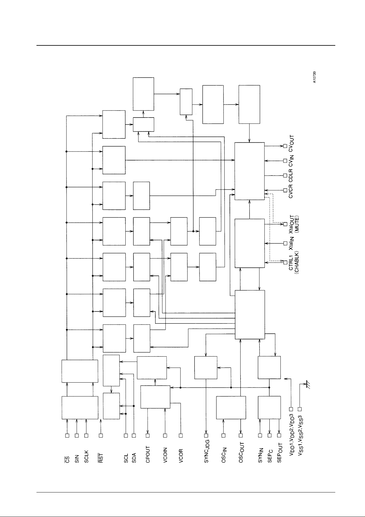
System Block Diagram
No. 5919-8/35
LC74775, 74775M
RAM write
address
counter
Display RAM
Deco-
der
Decoder
Font ROM
Display
control
register
Shift register
Character output control
Background control
Video output control
Sync signal generator
Blinking and
reverse
video control
register
Vertical
display
position
register
Horizontal
display
position
register
Blinking and
reverse video
control circuit
Vertical dot
counter
Horizontal
dot counter
Vertical display
position
detector
Line control
counter
Horizontal
display position
detector
Character
control
counter
Vertical size
counter
Horizontal
size counter
Vertical
character
size register
Horizontal
character
size register
Output control
Data output
buffer
Data
slicer
circuit
AFC
circuit
8-bit latch
+
command
decoder
Serial to
parallel
converter
Sync
discrimina-
tion
Character
output dot
clock
generator
Composite
sync signal
separation
control
Sync
separator
data
separator
circuit
Timing generator
Page 9
Display Control Commands
Display control commands have an 8-bit format and are transferred using the serial input function. Commands consist of a
command identification code in the first byte and command data in the following bytes. The following commands are supported.
COMMAND0: Display memory (VRAM) write address setup command
COMMAND1: Display character data write command
COMMAND2: Vertical display start position and vertical character size setup command
COMMAND3: Horizontal display start position and horizontal character size setup command
COMMAND4: Display control setup command
COMMAND5: Display control setup command
COMMAND6: Synchronizing signal detection setup command
COMMAND7 to COMMAND12 and COMMAND18: Display control setup commands
COMMAND13 to COMMAND17: VPS/PDC control commands. These commands can only be written with the I2C bus
(the SCL and SDA pins).
Display Control Command Table
No. 5919-9/35
LC74775, 74775M
First byte Second byte
Command
Command identification code
Data Data
7 6 5 4 3 2 1 0 7 6 5 4 3 2 1 0
COMMAND0 1 0 0 0 V3 V2 V1 V0 0 0 0 H4 H3 H2 H1 H0
(Write address setup)
COMMAND1 1 0 0 1 0 0 0 0 at c6 c5 c4 c3 c2 c1 c0
(Character write)
COMMAND2 (Vertical character size and 1 0 1 0 VS VS VS VS 0 FS VP VP VP VP VP VP
vertical display start position) 21 20 11 10 5 4 3 2 1 0
COMMAND3 (Horizontal character size and 1 0 1 1 HS HS HS HS 0 LC HP HP HP HP HP HP
horizontal display start position) 21 20 11 10 5 4 3 2 1 0
COMMAND4 1 1 0 0 TST RAM OSC SYS 0 BLK BLK BLK BK BK RV DSP
(Display control) MOD ERS STP RST 2 1 0 1 0 ON
COMMAND5 1 1 0 1 NP NP NON INT 0 RSH HLF BCL CB PH PH PH
(Display control) 1 0 LV2 INT 2 1 0
COMMAND6 1 1 1 0 SEL MOD DIS MUT 0 RN RN RN SN SN SN SN
(Synchronizing signal detection) 0 0 LIN 2 1 0 3 2 1 0
COMMAND7 1 1 1 1 0 0 0 0 0 CIN CIN VNP VSP MSK MSK EGL
(Display control) SEL CTL SEL SEL ERS SEL
COMMAND8 1 1 1 1 0 0 0 1 0 LNA LNA LNA LNA LPA LPA LPA
(Display control) 3 2 1 0 2 1 0
COMMAND9 1 1 1 1 0 0 1 0 0 LNB LNB LNB LNB LPB LPB LPB
(Display control) 3 2 1 0 2 1 0
COMMAND10 1 1 1 1 0 0 1 1 0 LNC LNC LNC LNC LPC LPC LPC
(Display control) 3 2 1 0 2 1 0
COMMAND11 1 1 1 1 0 1 0 0 0 0 VSP VSP LNC MOD LNB MOD
(Display control) DCK SLC SEL 3 SEL 2
COMMAND12 1 1 1 1 0 1 0 1 0 0 OTD OTD HLF SEL OTH IND
(Display control) S1 S0 INT 2
COMMAND18 1 1 1 1 1 0 1 1 0 0 RNE SJN SJN SJN SJC SJC
(Display control) 0 3 2 1 1 0
COMMAND13 1 1 1 1 0 1 0 1 0 CPA CPA CPA VPM VPM VPM VPM
(VPS/PDC control) 2 1 0 3 2 1 0
COMMAND14 1 1 1 1 0 1 1 0 0 VMW VMW HBS HBS BMS EMS DCE
(VPS/PDC control) SE2 SEL 2 1
COMMAND15 1 1 1 1 0 1 1 1 0 0 ECV ECV ECV ECV ECV ECV
(VPS/PDC control) 15 14 13 12 11 5
COMMAND16 1 1 1 1 1 0 0 0 0 ECP ECP ECP ECP ECP ECP ECP
(VPS/PDC control) 19 18 17 16 15 14 13
COMMAND17 1 1 1 1 1 0 0 1 0 0 ECP ECP ECP ECP ECP ECP
(VPS/PDC control) 25 24 23 22 21 20
Once written, a first byte command identification code is stored until the next first byte is written. However, when the
display character data write command (COMMAND1) is written, the LC74775/M locks into the display character data
write mode, and another first byte cannot be written.
When the CS pin is set high, the LC74775/M is set to the COMMAND0 (display memory write address setup mode) state.
Page 10
COMMAND0 (Display memory write address setup command)
No. 5919-10/35
LC74775, 74775M
DA 0 to 7 Register
Contents
Notes
State Function
7 – 1
6 – 0 Command 0 identification code.
5 – 0 Display memory write address setup.
4 – 0
3 V3
0
1
2 V2
0
1 Display memory line address (0 to B hexadecimal)
1 V1
0
1
0 V0
0
1
• First byte
DA 0 to 7 Register
Contents
Notes
State Function
7 – 0 Second byte identification bit
6 – 0
5 – 0
4 H4
0
1
3 H3
0
1
2 H2
0 Display memory column address (0 to 17 hexadecimal)
1
1 H1
0
1
0 H0
0
1
• Second byte
Note: All registers are set to 0 when the LC74775/M is reset by the RST pin.
DA 0 to 7 Register
Contents
Notes
State Function
7 – 1
When this command is input, the LC74775/M
6 – 0 Command 1 identification code.
locks in the display character data write mode
5 – 0 Display character data write mode setup.
until the CS pin goes high.
4 – 1
3 – 0
2 – 0
1 – 0
0 – 0
• First byte
COMMAND1 (Display character data write setup command)
Page 11
No. 5919-11/35
LC74775, 74775M
DA 0 to 7 Register
Contents
Notes
State Function
7 at
0 Character attribute off
1 Character attribute on
6 c6
0
1
5 c5
0
1
4 c4
0
1 Character code (00 to 7F hexadecimal)
3 c3
0
1
2 c2
0 (7E
HEX
: Space character)
1 (7F
HEX
: Transparent space character)
1 c1
0
1
0 c0
0
1
• Second byte
Note: All registers are set to 0 when the LC74775/M is reset by the RST pin.
DA 0 to 7 Register
Contents
Notes
State Function
7 – 1
6 – 0
Command 2 identification code.
5 – 1
Vertical display start position and the vertical character
4 – 0
size setup.
3 VS21
0
1
Second line vertical character size
2 VS20
0
1
1 VS11
0
1
First line vertical character size
0 VS10
0
1
COMMAND2: Vertical display start position and vertical character size setup command
VS20
0 1
VS21
0 1H/dot 2H/dot
1 3H/dot 1H/dot
VS10
0 1
VS11
0 1H/dot 2H/dot
1 3H/dot 1H/dot
DA 0 to 7 Register
Contents
Notes
State Function
7 – 0 Second byte identification bit
6 FS
0 Crystal oscillator frequency: 2fsc
1 Crystal oscillator frequency: 4fsc
5
VP5 0
(MSB) 1
4 VP4
0
1
3 VP3
0 The vertical display start position is set by the
1 6 bits VP0 to VP5.
2 VP2
0 The weight of bit 1 is 2H.
1
1 VP1
0
1
0
VP0 0
(LSB) 1
• Second byte
If VS is the vertical display start position then:
VS = α +H ×
H: The horizontal synchronization pulse period
α = 20H (525H systems)
α = 25H (625H systems)
2 ∑ 2 VP
n
5
n
n=0
Character display area
Note: All registers are set to 0 when the LC74775/M is reset by the RST pin.
• First byte
Page 12

No. 5919-12/35
LC74775, 74775M
DA 0 to 7 Register
Contents
Notes
State Function
7 – 1
6 – 0
Command 3 identification code.
5 – 1
Horizontal display start position and the horizontal
4 – 1
character size setup.
3 HS21
0
1
Second line horizontal character size
2 HS20
0
1
1 HS11
0
1
First line horizontal character size
0 HS10
0
1
• First byte
VS20
0 1
VS21
0 1Tc/dot 2Tc/dot
1 3Tc/dot 1Tc/dot
VS10
0 1
VS11
0 1Tc/dot 2Tc/dot
1 3Tc/dot 1Tc/dot
COMMAND3 (Horizontal display start position and horizontal size setup command)
DA 0 to 7 Register
Contents
Notes
State Function
7 – 0 Second byte identification bit
6 LC
0 Use the LC oscillator as the dot clock
Selects the dot clock used for character
1 Use the crystal oscillator as the dot clock
display in the horizontal direction.
5
HP5 0
(MSB) 1
4 HP4
0
1
3 HP3
0
The horizontal display start position is set
1 by the 6 bits HP0 to HP5.
2 HP2
0
The weight of bit 1 is 2Tc.
1
1 HP1
0
1
0
HP0 0
(LSB) 1
• Second byte
Note: All registers are set to 0 when the LC74775/M is reset by the RST pin.
If HS is the horizontal start position then:
HS = Tc ×
Tc: Period of the oscillator connected to OSCIN/OSCOUT
in operating mode.
2 ∑ 2 HP
n
5
n
n=0
Page 13

No. 5919-13/35
LC74775, 74775M
DA 0 to 7 Register
Contents
Notes
State Function
7 – 1
6 – 1 Command 4 identification code.
5 – 0 Display character data write setup.
4 – 0
3 TSTMOD
0 Normal operating mode
This bit must be set to 0
1 Test mode
2 RAMERS
0
Erasing RAM takes about 500 µs. (This operation
1
Erase display RAM.(The RAM data is set to 7F hexadecimal.)
must be executed in the DSPOFF state.)
1 OSCSTP
0 Do not stop the crystal and VCO oscillators
Valid in external synchronization mode when
1 Stop the crystal and VCO oscillators
character display is off
0
The registers are reset when the CS pin is
0 SYSRST
1 Reset all registers and turn display off
low, and the reset state is cleared when CS
is set high.
• First byte
COMMAND4 (Display control setup command)
DA 0 to 7 Register
Contents
Notes
State Function
7 – 0 Second byte identification bit
6 BLK2
0 Character display area
Specifies the size for complete fill in
1 Video display area
5 BLK1
0
1
Changes the blanking size
4 BLK0
0
1
3 BK1
0 Blinking period: About 0.5 s
Switches the blinking period
1 Blinking period: About 1.0 s
2 BK0
0 Blinking off
1 Blinking on
1 RV
0 Reverse video off
1 Reverse video on
0 DSPON
0 Character display off
1 Character display on
• Second byte
Note: All registers are set to 0 when the LC74775/M is reset by the RST pin.
BLK0
0 1
BLK1
0 Blanking off Character size
1 Frame size Complete fill in size
Blinking in character reverse video mode
switches the display between normal
character display and reverse video display
Page 14

No. 5919-14/35
LC74775, 74775M
DA 0 to 7 Register
Contents
Notes
State Function
7 – 1
6 – 1 Command 5 identification code.
5 – 0 Display control setup.
4 – 1
3 NP1
0 NTSC
Switches between NTSC and PAL
1 PAL
2 NP0
0 525 lines
Modified by the external input signal V
1 625 lines
1 NON
0 Interlaced
Switches between interlaced and
1 Noninterlaced
noninterlaced video
0 INT
0 External synchronization
Switches between external and internal
1 Internal synchronization
synchronization
• First byte
COMMAND5 (Display control setup command)
DA 0 to 7 Register
Contents
Notes
State Function
7 – 0 Second byte identification bit
6 RSHLV2
0 Background color level 1. (Level that is different from blue.)
Switches the background color signal level
1
Background color level 2. (Level that is identical to the blue level.)
5 HLFINT
0 Normal mode
1 Partial internal synchronization mode
4 BCL
0 Background color on
Only valid in internal synchronization mode
1 No background color. (Only the background level is set.)
3 CB
0 Color burst signal output
Only valid when BCL is high
1 Color burst signal output stopped
0
2 PH2
1
0
1 PH1 Background color specification
1
0
0 PH0
1
• Second byte
PH2 PH1
PH0
Background color
(phase)
0 0 0 Cyan
0 0 1 Yellow
0 1 0 Red
0 1 1 Blue
1 0 0 Cyan - blue
1 0 1 Green
1 1 0 Orange
1 1 1 Magenta
Note: All registers are set to 0 when the LC74775/M is reset by the RST pin.
Page 15

No. 5919-15/35
LC74775, 74775M
DA 0 to 7 Register
Contents
Notes
State Function
7 – 1
6 – 1 Command 6 identification code.
5 – 1 Synchronizing signal control setup.
4 – 0
3 SEL0
0
1
0 Switches the SEP
OUT
(pin 19) output
2 MOD0
1
1 DISLIN
0 12 lines
Switches the number of lines displayed
1 10 lines
0 MUT
0 Normal output
CV
OUT
switching
1 CV
IN
is cut and CV
OUT
is held at the pedestal level
• First byte
SEL0 MOD0 SEPOUT
0 0 DAV
0 1 Sliced data width
1 0 CSYNC
1 1 ST pulse signal
COMMAND6 (Synchronizing signal detection setup command)
DA 0 to 7 Register
Contents
Notes
State Function
7 – 0 Second byte identification bit
6 RN2
0
1
5 RN1
0
1
4 RN0
0
1
3 SN3
0
1
2 SN2
0
1
1 SN1
0
1
0 SN0
0
1
• Second byte
RN2 RN1 RN0 Number of times HSYNC detected
0 0 0 0 (32)
0 0 1 4 (64)
0 1 0 8 (128)
1 0 0 16 (256)
SN3 SN2 SN1 SN0 Number of times HSYNC detected
0 0 0 0 Not output
0 0 0 1 32
0 0 1 0 64
0 1 0 0 128
1 0 0 0 256
External synchronizing signal detection control.
Signal absent → signal present transition
detection.
Sets the sampling period in which SYNC can
be detected continuously in the horizontal
synchronizing signal period (1H).
Values in parentheses apply when RNE0
(COM18) is 1.
External synchronizing signal detection
control.
Signal present → signal absent transition
detection.
Sets the sampling period in which SYNC
cannot be detected continuously in the
horizontal synchronizing signal period (1H).
Note: All registers are set to 0 when the LC74775/M is reset by the RST pin.
Page 16

No. 5919-16/35
LC74775, 74775M
DA 0 to 7 Register
Contents
Notes
State Function
7 – 1
6 – 1 Command 7 identification code.
5 – 1 Display control setup.
4 – 1
3 – 0
2 – 0
Extended command 0 identification code
1 – 0
0 – 0
• First byte
COMMAND7 (Display control setup command)
DA 0 to 7 Register
Contents
Notes
State Function
7 0 Second byte identification bit
6
CINSEL
0
Blank area (The logical OR of the character and frame signals)
CVCRon signal switching
1 Video signal display area
5 CINCTL
0 CV
CR
: off
CV
CR
on/off switching
1 CV
CR
: on
4 VNPSEL
0 V falling edge detection
Switches the V acquisition polarity in external
1 V rising edge detection
mode when internal V separation is used.
3 VSPSEL
0 VSEP: about 8.9 µs (NTSC)
Switches the internal V separation period
1 VSEP: about 17.8 µs (NTSC)
2 MSKERS
0 Mask valid
Clears the HSYNC and VSYNK masks
1 Mask invalid
1 MSKSEL
0 3H (NTSC)
Switches the VSYNC mask
1 20H (NTSC)
0 EGL
0 Frame level 0 only (VBK0)
Switches the frame level.
1 Two-stage frame level (VBK0 and VBK1)
(Only valid when BLK0 is 0 and BLK1 is 1.)
• Second byte
Note: All registers are set to 0 when the LC74775/M is reset by the RST pin.
Page 17

No. 5919-17/35
LC74775, 74775M
DA 0 to 7 Register
Contents
Notes
State Function
7 – 1
6 – 1 Command 7 identification code.
5 – 1 Display control setup.
4 – 1
3 – 0
2 – 0
Extended command 1 identification code
1 – 0
0 – 1
• First byte
COMMAND8 (Display control setup command)
DA 0 to 7 Register
Contents
Notes
State Function
7 – 0 Second byte identification bit
0
6 LNA3
1
0
5 LNA2
1
0
4 LNA1
1
0
3 LNA0
1
0
2 LPA2
1
0
1 LPA1 Specifies the background color
1
0
0 LPA0
1
• Second byte
LPA2 LPA1 LPA0 Line background color (phase)
0 0 0 Cyan
0 0 1 Yellow
0 1 0 Red
0 1 1 Blue
1 0 0 Cyan - blue
1 0 1 Green
1 1 0 Orange
1 1 1 Magenta
LNA3 LNA2 LNA1 LNA0 Specified line
0 0 0 0 Do not change the line background
0 0 0 1 Line 1
0 0 1 0 Line 2
0 0 1 1 Line 3
0 1 0 0 Line 4
0 1 0 1 Line 5
0 1 1 0 Line 6
0 1 1 1 Line 7
1 0 0 0 Line 8
1 0 0 1 Line 9
1 0 1 0 Line 10
1 0 1 1 Line 11
1 1 – – Line 12
Specifies the line whose background is to be
changed.
(When the background color is specified for
the same line with LNA*, LNB*, and LNC*,
the command specified last becomes valid.
The previously specified registers (LN* and
LP*) are all cleared to 0.)
Note: All registers are set to 0 when the LC74775/M is reset by the RST pin.
Page 18

No. 5919-18/35
LC74775, 74775M
• First byte
COMMAND9 (Display control setup command)
DA 0 to 7 Register
Contents
Notes
State Function
7 – 0 Second byte identification bit
0
6 LNB3
1
0
5 LNB2
1
0
4 LNB1
1
0
3 LNB0
1
0
2 LPB2
1
0
1 LPB1 Specifies the background color
1
0
0 LPB0
1
• Second byte
LPC2 LPC1 LPC0 Line background color (phase)
0 0 0 Cyan
0 0 1 Yellow
0 1 0 Red
0 1 1 Blue
1 0 0 Cyan - blue
1 0 1 Green
1 1 0 Orange
1 1 1 Magenta
LNB3 LNB2 LNB1 LNB0 Specified line
0 0 0 0 Do not change the line background
0 0 0 1 Line 1
0 0 1 0 Line 2
0 0 1 1 Line 3
0 1 0 0 Line 4
0 1 0 1 Line 5
0 1 1 0 Line 6
0 1 1 1 Line 7
1 0 0 0 Line 8
1 0 0 1 Line 9
1 0 1 0 Line 10
1 0 1 1 Line 11
1 1 – – Line 12
Specifies the line whose background is to be
changed.
(When the background color is specified for
the same line with LNA*, LNB*, and LNC*,
the command specified last becomes valid.
The previously specified registers (LN* and
LP*) are all cleared to 0.)
Note: All registers are set to 0 when the LC74775/M is reset by the RST pin.
DA 0 to 7 Register
Contents
Notes
State Function
7 – 1
6 – 1 Command 7 identification code.
5 – 1 Display control setup.
4 – 1
3 – 0
2 – 0
Extended command 2 identification code
1 – 1
0 – 0
Page 19

No. 5919-19/35
LC74775, 74775M
• First byte
COMMAND10 (Display control setup command)
DA 0 to 7 Register
Contents
Notes
State Function
7 – 0 Second byte identification bit
0
6 LNC3
1
0
5 LNC2
1
0
4 LNC1
1
0
3 LNC0
1
0
Specifies the background color
2 LPC2
1
0
1 LPC1
1
0
0 LPC0
1
• Second byte
LPB2 LPB1 LPB0 Line background color (phase)
0 0 0 Cyan
0 0 1 Yellow
0 1 0 Red
0 1 1 Blue
1 0 0 Cyan - blue
1 0 1 Green
1 1 0 Orange
1 1 1 Magenta
LNB3 LNB2 LNB1 LNB0 Specified line
0 0 0 0 Do not change the line background
0 0 0 1 Line 1
0 0 1 0 Line 2
0 0 1 1 Line 3
0 1 0 0 Line 4
0 1 0 1 Line 5
0 1 1 0 Line 6
0 1 1 1 Line 7
1 0 0 0 Line 8
1 0 0 1 Line 9
1 0 1 0 Line 10
1 0 1 1 Line 11
1 1 – – Line 12
Specifies the line whose background is to be
changed.
(When the background color is specified for
the same line with LNA*, LNB*, and LNC*,
the command specified last becomes valid.
The previously specified registers (LN* and
LP*) are all cleared to 0.)
Note: All registers are set to 0 when the LC74775/M is reset by the RST pin.
DA 0 to 7 Register
Contents
Notes
State Function
7 – 1
6 – 1 Command 7 identification code.
5 – 1 Display control setup.
4 – 1
3 – 0
2 – 0
Extended command 3 identification code
1 – 1
0 – 1
Page 20

No. 5919-20/35
LC74775, 74775M
DA 0 to 7 Register
Contents
Notes
State Function
7 – 1
6 – 1 Command 7 identification code.
5 – 1 Display control setup.
4 – 1
3 – 0
2 – 1
Extended command 4 identification code
1 – 0
0 – 0
• First byte
COMMAND11 (Display control setup command)
DA 0 to 7 Register
Contents
Notes
State Function
7 – 0 Second byte identification bit
6 – 0
5 VSPDCK
0 LC oscillator: operating
LC oscillator control
1 LC oscillator: stopped
4 VSPSLC
0 VCO: operating
VCO control
1 VCO: stopped
0 Normal line background color operation
Switches the RV mode background color for RV
3 LNCSEL 1
RV characters have the background color specified by
specified characters in LNC* specified lines
PH* and the RV character background color is white
0 The LNCSEL = 1 setting specifications
2 MOD3
1
RV characters have the background color specified by PH*
Valid when LNCSEL is high
and characters are white
0 Normal line background color operation
Switches the RV mode background color for RV
1 LNBSEL
1
RV characters have the background color specified by PH*
specified characters in LNB* specified lines
and the RV character background color is white
0 The LNBSEL = 1 setting specifications
0 MOD2
1
RV characters have the background color specified by PH*
Valid when LNBSEL is high
and characters are white
• Second byte
Note: All registers are set to 0 when the LC74775/M is reset by the RST pin.
Page 21

No. 5919-21/35
LC74775, 74775M
DA 0 to 7 Register
Contents
Notes
State Function
7 – 0 Second byte identification bit
6 – 0
5 OTDCS1
0
1
External synchronization mode dot clock setting
4 OTDCS0
0
1
3 HLFTON
0
1
0
2 SEL2
1
1 OTHS
0 CSYNCB (sync separator)
External synchronization mode H input switching
1 HDB (slicer AFC)
0 IND3
0 LC oscillator
Internal synchronization mode dot clock setup
1 Crystal oscillator
OTDS1 OTDS0 Dot clock
0 0 LC oscillator
0 1 Crystal oscillator
1 0 VCO
DA 0 to 7 Register
Contents
Notes
State Function
7 – 1
6 – 1 Command 7 identification code.
5 – 1 Display control setup.
4 – 1
3 – 0
2 – 1
Extended command 5 identification code
1 – 0
0 – 1
• First byte
COMMAND12 (Display control setup command)
• Second byte
SEL2 HLFTON Output
0 0 SYNC
JDG
0 1 Halftone
1 0 LOCK
1 1 SYNCDET
SYNC
JDG
pin (pin 8) output switching.
The halftone output line specification depends
on background color specification (the logical
OR of the 3-line specification).
Note: All registers are set to 0 when the LC74775/M is reset by the RST pin.
Page 22

No. 5919-22/35
LC74775, 74775M
DA 0 to 7 Register
Contents
Notes
State Function
7 – 1
6 – 1 Command 7 identification code.
5 – 1 Display control setup.
4 – 1
3 – 1
2 – 0
Extended command B identification code
1 – 1
0 – 1
• First byte
COMMAND18 (Display control setup command)
DA 0 to 7 Register
Contents
Notes
State Function
7 – 0 Second byte identification bit
6 – 0
0 Sync discrimination signal absent → present: normal value
5 RNE0
1
0
4 SJNS3
1
0
3 SJNS2
1
0
2 SJNS1
1
1 SJCS1
0
1
0 SJCS0
0
1
• Second byte
Setting for the noise rejection circuit used for
sync discrimination signal absent → present
transition.
The sync signal absent state is recognized
when the number of high-level signals shown
in the table is input during a 1H period.
Note: All registers are set to 0 when the LC74775/M is reset by the RST pin.
Changes the discrimination value for the sync
discrimination signal absent → present
transition
Sync discrimination.
HSYNI signal extraction clock selection.
Sync discrimination signal absent → present: value shown
in parentheses
SJNS3 SJNS2 SJNS1 Number of times
0 0 0 None
0 0 1 4
0 1 0 8
0 1 1 16
1 0 0 32
1 0 1 64
1 1 0 128
1 1 1 256
SJCS1 SJCS0 PAL NTSC
0 0 677 ns (1/3) 558 ns (1/2)
0 1 903 ns (1/4) 838 ns (1/3)
1 0 450 ns (1/2) 1117 ns (1/4)
Page 23

No. 5919-23/35
LC74775, 74775M
DA 0 to 7 Register
Contents
Notes
State Function
7 – 1
6 – 1 Command 7 identification code.
5 – 1 Display control setup.
4 – 1
3 – 0
2 – 1
Extended command 5 identification code
1 – 0
0 – 1
• First byte
COMMAND13 (VPS/PDC control setup command) I2C bus only
DA 0 to 7 Register
Contents
Notes
State Function
7 – 0 Second byte identification bit
6 CPA2
0
1
5 CPA1
0
1
4 CPA0
0
1
0
3 VPM3
1
0
2 VPM2
1
Slicer mode selection
0
1 VPM1
1
0
0 VPM0
1
CPA2 CPA1 CPA0 Clock
0 0 0 No. 1
0 0 1 No. 2
0 1 0 No. 3
0 1 1 No. 4
1 0 0 No. 5
1 0 1 No. 6
1 1 0 No. 7
1 1 1 No. 8
• Second byte
Note: All registers are set to 0 when the LC74775/M is reset by the RST pin.
M3 M2 M1 M0 Operating mode
0 0 0 0 VPS
0 0 0 1 8/30/2 (PDC)
0 0 1 0 Automatic PDC/VPS discrimination 1
0 0 1 1 8/30/1 (UDT)
0 1 0 0 Header time 1
0 1 0 1 Header time 2
0 1 1 0 Header time 3
0 1 1 1 Header time 4
1 0 0 0 Status display 1
1 0 0 1 Status display 2
1 0 1 0 Status display 3
1 0 1 1 Status display 4
1 1 0 0 PAL Pulse
1 1 0 1 Automatic PDC/VPS discrimination 2
1 1 1 0 Automatic PDC/VPS discrimination 3
1 1 1 1 Automatic PDC/VPS discrimination 4
Data acquisition clock selection.
Shifts in multiples of 8 clock units with
respect to the data.
Page 24

No. 5919-24/35
LC74775, 74775M
DA 0 to 7 Register
Contents
Notes
State Function
7 – 1
6 – 1 Command 7 identification code.
5 – 1 Display control setup.
4 – 1
3 – 0
2 – 1
Extended command 6 identification code
1 – 1
0 – 0
• First byte
COMMAND14 (VPS/PDC control setup command) I2C bus only
DA 0 to 7 Register
Contents
Notes
State Function
7 – 0 Second byte identification bit
6 VMWSE2
0 V mask period start - From the retrace period
CPOUT pin (pin 13) V mask period switching 2
1 V mask period start - From 10H before the retrace period
5 VMWSEL
0 The V mask period is the retrace period
CPOUT pin (pin 13) V mask period switching
1 The V mask period is 9H
4 HBS2
0 Clock running discrimination 1 (2 times)
Clock running discrimination count setting
1 Clock running discrimination 2 (4 times)
3 HBS1
0 Framing code discrimination 1
Framing code discrimination selection
1 Framing code discrimination 2 (Single bad bits are ignored)
0
Error check valid (Error checking can be turned on or
2 BMS
off on a per-byte basis.)
1
Error check invalid (Applications can select whether data for
which an error is detected is held or writing on a per-byte basis.)
0 Data hold
1 EMS
1
Data write
(When the error bit is 0 in VPS mode.)
Error checking enabled for unused data bytes.
0
VPS: bytes 3, 4, and 6 to 10, PDC: bytes 7 to 12, header 1:
bytes 14 to 37, header 2: bytes 14 to 29, header 3: bytes 14
0 DCE
to 21, status 1 (3): bytes 7 to 25, status 2 (4): bytes 7 to 35
Error checking disabled for unused data bytes.
1
VPS: bytes 3, 4, and 6 to 10, PDC: bytes 7 to 12, header 1:
bytes 14 to 37, header 2: bytes 14 to 29, header 3: bytes 14
to 21, status 1 (3): bytes 7 to 25, status 2 (4): bytes 7 to 35
• Second byte
Note: All registers are set to 0 when the LC74775/M is reset by the RST pin.
When set to 0, if there are no errors in bytes
for which error checking is turned on, those
bytes are written to P-S. When set to 1, all
bytes are written to P-S regardless of the error
status.
Specifies handling of bytes for which error
checking is set to off but in which an error
occurred when error checking is turned on
Error checking setting for unused data bytes.
Biphase (VPS), Hamming (PDC), and odd
parity (header)
Page 25

No. 5919-25/35
LC74775, 74775M
DA 0 to 7 Register
Contents
Notes
State Function
7 – 1
6 – 1 Command 7 identification code.
5 – 1 Display control setup.
4 – 1
3 – 0
2 – 1
Extended command 7 identification code
1 – 1
0 – 1
• First byte
COMMAND15 (VPS/PDC control setup command) I2C bus only
DA 0 to 7 Register
Contents
Notes
State Function
7 – 0 Second byte identification bit
6 – 0
5 ECV15
0 Byte 15 biphase error check on (Data hold)
1 Byte 15 biphase error check off (Data write)
4 ECV14
0 Byte 14 biphase error check on (Data hold)
1 Byte 14 biphase error check off (Data write)
3 ECV13
0 Byte 13 biphase error check on (Data hold)
1 Byte 13 biphase error check off (Data write)
2 ECV12
0 Byte 12 biphase error check on (Data hold)
1 Byte 12 biphase error check off (Data write)
1 ECV11
0 Byte 11 biphase error check on (Data hold)
1 Byte 11 biphase error check off (Data write)
0 ECV5
0 Byte 5 biphase error check on (Data hold)
1 Byte 5 biphase error check off (Data write)
• Second byte
Note: All registers are set to 0 when the LC74775/M is reset by the RST pin.
Specification when the VPS data BMS bit is 0.
The item in parentheses is the specification
when the VPS data BMS bit is 1.
Page 26

No. 5919-26/35
LC74775, 74775M
DA 0 to 7 Register
Contents
Notes
State Function
7 – 1
6 – 1 Command 7 identification code.
5 – 1 Display control setup.
4 – 1
3 – 1
2 – 0
Extended command 8 identification code
1 – 0
0 – 0
• First byte
COMMAND16 (VPS/PDC control setup command) I2C bus only
DA 0 to 7 Register
Contents
Notes
State Function
7 – 0 Second byte identification bit
0
Byte 19 Hamming error check on (Data hold)
6 ECP19
{Bytes 44, 28, 36, 20, 32, 42, 32, and 42}
1
Byte 19 Hamming error check off (Data write)
{Bytes 44, 28, 36, 20, 32, 42, 32, and 42}
0
Byte 18 Hamming error check on (Data hold)
5 ECP18
{Bytes 43, 27, 35, 19, 31, 41, 31, and 41}
1
Byte 18 Hamming error check off (Data write)
{Bytes 43, 27, 35, 19, 31, 41, 31, and 41}
0
Byte 17 Hamming error check on (Data hold)
4 ECP17
{Bytes 42, 26, 34, 18, 30, 40, 30, and 40}
1
Byte 17 Hamming error check off (Data write)
{Bytes 42, 26, 34, 18, 30, 40, 30, and 40}
0
Byte 16 Hamming error check on (Data hold)
3 ECP16
{Bytes 41, 25, 33, 17, 29, 39, 29, and 39}
1
Byte 16 Hamming error check off (Data write)
{Bytes 41, 25, 33, 17, 29, 39, 29, and 39}
0
Byte 15 Hamming error check on (Data hold)
2 ECP15
{Bytes 40, 24, 32, 16, 28, 38, 28, and 38}
1
Byte 15 Hamming error check off (Data write)
{Bytes 40, 24, 32, 16, 28, 38, 28, and 38}
0
Byte 14 Hamming error check on (Data hold)
1 ECP14
{Bytes 39, 23, 31, 15, 27, 37, 27, and 37}
1
Byte 14 Hamming error check off (Data write)
{Bytes 39, 23, 31, 15, 27, 37, 27, and 37}
0
Byte 13 Hamming error check on (Data hold)
0 ECP13
{Bytes 38, 22, 30, 14, 26, 36, 26, and 36}
1
Byte 13 Hamming error check off (Data write)
{Bytes 38, 22, 30, 14, 26, 36, 26, and 36}
• Second byte
Note: All registers are set to 0 when the LC74775/M is reset by the RST pin.
Specification when the PDC data BMS bit is 0.
The item in parentheses is the specification
when the BMS bit is 1.
The item in curly braces lists the odd parity
check on/off bytes for header modes 1, 2, 3,
and 4 and status mode 1, 2, 3, and 4.
Page 27

No. 5919-27/35
LC74775, 74775M
DA 0 to 7 Register
Contents
Notes
State Function
7 – 1
6 – 1 Command 7 identification code.
5 – 1 Display control setup.
4 – 1
3 – 1
2 – 0
Extended command 9 identification code
1 – 0
0 – 1
• First byte
COMMAND17 (VPS/PDC control setup command) I2C bus only
DA 0 to 7 Register
Contents
Notes
State Function
7 – 0 Second byte identification bit
6 – 0
0 Byte 25 Hamming error check on (Data hold)
5 ECP25
1 Byte 25 Hamming error check off (Data write)
0 Byte 24 Hamming error check on (Data hold)
4 ECP24
1 Byte 24 Hamming error check off (Data write)
0 Byte 23 Hamming error check on (Data hold)
3 ECP23
1 Byte 23 Hamming error check off (Data write)
0
Byte 22 Hamming error check on (Data hold)
2 ECP22
{Bytes , , , , 35, 45, 35, and 45}
1
Byte 22 Hamming error check off (Data write)
{Bytes , , , , 35, 45, 35, and 45}
0
Byte 21 Hamming error check on (Data hold)
1 ECP21
{Bytes , , , , 34, 44, 34, and 44}
1
Byte 21 Hamming error check off (Data write)
{Bytes , , , , 34, 44, 34, and 44}
0
Byte 20 Hamming error check on (Data hold)
0 ECP20
{Bytes 45, 29, 37, 21, 33, 43, 33, and 43}
1
Byte 20 Hamming error check off (Data write)
{Bytes 45, 29, 37, 21, 33, 43, 33, and 43}
• Second byte
Note: All registers are set to 0 when the LC74775/M is reset by the RST pin.
Specification when the PDC data BMS bit is 0.
The item in parentheses is the specification
when the BMS bit is 1.
The item in curly braces lists the odd parity
check on/off bytes for header modes 1, 2, 3,
and 4 and status mode 1, 2, 3, and 4.
Page 28

No. 5919-28/35
LC74775, 74775M
PDC/VPS Output Data Format
Data is output in order starting with bit 7 of byte 1.
Output data
PDC 8/30 mode
VPS mode Header time mode 1 (3) Header time mode 2 (4)
Format 1 Format 2
Byte 1 Bit 7 byte 15 bit 0 byte 16 bit 0 byte 11 bit 0 byte 38 bit 0 byte 22 bit 0
6 1 1 1 (30) 1 (14) 1
5 2 2 2 2 2
4 3 3 3 3 3
3 4 byte17 bit 0 4 4 4
2 5 1 5 5 5
1 6 2 6 6 6
0 7 3 7 7 7
Byte 2 Bit 7 byte 16 bit 0 byte 18 bit 0 byte 12 bit 0 byte 39 bit 0 byte 23 bit 0
6 1 1 1 (31) 1 (15) 1
5 2 2 2 2 2
4 3 3 3 3 3
3 4 byte19 bit 0 4 4 4
2 5 1 5 5 5
1 6 2 6 6 6
0 7 3 7 7 7
Byte 3 Bit 7 byte 17 bit 0 byte 20 bit 0 byte 13 bit 0 byte 40 bit 0 byte 24 bit 0
6 1 1 1 (32) 1 (16) 1
5 2 2 2 2 2
4 3 3 3 3 3
3 4 byte 21 bit 0 4 4 4
2 5 1 5 5 5
1 6 2 6 6 6
0 7 3 7 7 7
Byte 4 Bit 7 byte 18 bit 0 byte 22 bit 0 byte 14 bit 0 byte 41 bit 0 byte 25 bit 0
6 1 1 1 (33) 1 (17) 1
5 2 2 2 2 2
4 3 3 3 3 3
3 4 byte 23 bit 0 4 4 4
2 5 1 5 5 5
1 6 2 6 6 6
0 7 3 7 7 7
Byte 5 Bit 7 byte 19 bit 0 byte 14 bit 0 byte 5 bit 0 byte 42 bit 0 byte 26 bit 0
6 1 1 1 (34) 1 (18) 1
5 2 2 2 2 2
4 3 3 3 3 3
3 4 byte 15 bit 0 4 4 4
2 5 1 5 5 5
1 6 2 6 6 6
0 7 3 7 7 7
Byte 6 Bit 7 byte 20 bit 0 byte 24 bit 0 byte 15 bit 0 byte 43 bit 0 byte 27 bit 0
6 1 1 1 (35) 1 (19) 1
5 2 2 2 2 2
4 3 3 3 3 3
3 4 byte 25 bit 0 4 4 4
2 5 1 5 5 5
1 6 2 6 6 6
0 7 3 7 7 7
Continued on next page.
Page 29

Continued from preceding page.
No. 5919-29/35
LC74775, 74775M
Output data
PDC 8/30 mode
VPS mode Header time mode 1 (3) Header time mode 2 (4)
Format 1 Format 2
Byte 7 Bit 7 byte 21 bit 0 byte 13 bit 0 1 byte 44 bit 0 byte 28 bit 0
6 1 1 1 (36) 1 (20) 1
5 2 2 1 2 2
4 3 3 1 3 3
3 4 1 1 4 4
2 5 1 1 5 5
1 6 1 1 6 6
0 7 1 0 7 7
Byte 8 Bit 7 byte 13 bit 0 Error byte 16 Error byte 11 byte 45 bit 0 byte 29 bit 0
6 1
information 1
17
information
12 (37) 1 (21) 1
5 2 18 13 2 2
4 3 19 14 3 3
3 4 20 5 4 4
2 5 21 15 5 5
1 6 22 0 6 6
0 7 23 0 7 7
Byte 9 Bit 7 byte 14 bit 0 Error 14 Error byte 38 (30) Error byte 22 (14)
6 1
information 2
15
information
39 (31)
information
23 (15)
5 2 24 40 (32) 24 (16)
4 3 25 41 (33) 25 (17)
3 4 13 42 (34) 26 (18)
2 5 0 43 (35) 27 (19)
1 6 0 44 (36) 28 (20)
0 7 0 45 (37) 29 (21)
Byte 10 Bit 7 byte 22 bit 0
6 1
5 2
4 3
3 4
2 5
1 6
0 7
Byte 11 Bit 7 byte 23 bit 0
6 1
5 2
4 3
3 4
2 5
1 6
0 7
Byte 12 Bit 7 byte 24 bit 0
6 1
5 2
4 3
3 4
2 5
1 6
0 7
Byte 13 Bit 7 byte 25 bit 0
6 1
5 2
4 3
3 4
2 5
1 6
0 7
Note: A value of 1 is output for section with no output data setting.
Page 30

No. 5919-30/35
LC74775, 74775M
Data is output in order starting with bit 7 of byte 1.
Status display 1 and 2: 8/30/2 - Status display 1 and 2: 8/30/1
Output data Status display mode 1 (3) Status display mode 2 (4) PAL Puls
Byte 1 Bit 7 byte 26 bit 0 byte 36 bit 0 bit 0
6 (26) 1 (36) 1 1
5 2 2 2
4 3 3 3
3 4 4 4
2 5 5 5
1 6 6 6
0 7 7 7
Byte 2 Bit 7 byte 27 bit 0 byte 37 bit 0 bit 8
6 (27) 1 (37) 1 9
5 2 2 10
4 3 3 11
3 4 4 12
2 5 5 13
1 6 6 0
0 7 7 0
Byte 3 Bit 7 byte 28 bit 0 byte 38 bit 0
6 (28) 1 (38) 1
5 2 2
4 3 3
3 4 4
2 5 5
1 6 6
0 7 7
Byte 4 Bit 7 byte 29 bit 0 byte 39 bit 0
6 (29) 1 (39) 1
5 2 2
4 3 3
3 4 4
2 5 5
1 6 6
0 7 7
Byte 5 Bit 7 byte 30 bit 0 byte 39 bit 0
6 (30) 1 (40) 1
5 2 2
4 3 3
3 4 4
2 5 5
1 6 6
0 7 7
Byte 6 Bit 7 byte 31 bit 0 byte 41 bit 0
6 (31) 1 (41) 1
5 2 2
4 3 3
3 4 4
2 5 5
1 6 6
0 7 7
Byte 7 Bit 7 byte 32 bit 0 byte 42 bit 0
6 (32) 1 (42) 1
5 2 2
4 3 3
3 4 4
2 5 5
1 6 6
0 7 7
Continued on next page.
Page 31

No. 5919-31/35
LC74775, 74775M
Continued from preceding page.
Output data Status display mode 1 (3) Status display mode 2 (4) PAL Puls
Byte 8 Bit 7 byte 33 bit 0 byte 43 bit 0
6 (33) 1 (43) 1
5 2 2
4 3 3
3 4 4
2 5 5
1 6 6
0 7 7
Byte 9 Bit 7 byte 34 bit 0 byte 44 bit 0
6 (34) 1 (44) 1
5 2 2
4 3 3
3 4 4
2 5 5
1 6 6
0 7 7
Byte 10 Bit 7 byte 35 bit 0 byte 45 bit 0
6 (35) 1 (45) 1
5 2 2
4 3 3
3 4 4
2 5 5
1 6 6
0 7 7
Byte 11 Bit 7 Error byte 26 (26) Error byte 36 (36)
6
information 1
27 (27)
information 1
37 (37)
5 28 (28) 38 (38)
4 29 (29) 39 (39)
3 30 (30) 40 (40)
2 31 (31) 41 (41)
1 32 (32) 42 (42)
0 33 (33) 43 (43)
Byte 12 Bit 7 Error byte 34 (34) Error byte 44 (44)
6
information 2
35 (35)
information 1
45 (45)
5 0 0
4 0 0
3 0 0
2 0 0
1 0 0
0 0 0
Byte 13 Bit 7
6
5
4
3
2
1
0
Note: A value of 1 is output for section with no output data setting.
Page 32

Display Screen Structure
The display consists of 12 lines of 24 characters.
Up to 288 characters can be displayed.
The number of characters that can be displayed is reduced from the 288 maximum when enlarged characters are
displayed.
Display memory addresses are specified as row (0 to 11 decimal) and column (0 to 23 decimal) addresses.
Display Screen Structure (display memory addresses)
No. 5919-32/35
LC74775, 74775M
12 Rows
24 Characters
Page 33

Composite Video Signal Output Levels (internally generated levels)
CV
OUT
output level waveform (VDD2 = 5.00 V)
No. 5919-33/35
LC74775, 74775M
Output level Output voltage (1) [V] Output voltage (2) [V] Output voltage (3) [V]
V
CHA
: Character 2.65 2.85 3.25
V
RSH0
: Background colors other than blue: high 2.37 2.57 2.97
V
RSH1, 2
: Blue background colors 1 and 2: high 2.01 2.21 2.61
V
CBH
: Color burst high 1.67 1.87 2.27
V
RSL0
: Background colors other than blue: low 1.23 1.43 1.83
V
RSL1
: Blue background color 1: low 1.16 1.36 1.76
V
RSL2
: Blue background color 2: low 1.52 1.72 2.12
V
BK1
: Frame 1 2.08 2.28 2.68
V
BK0
: Frame 2 1.50 1.70 2.10
V
PD
: Pedestal 1.37 1.57 1.97
V
CBL
: Color burst low 1.07 1.27 1.67
V
SN
: Sync 0.80 1.00 1.40
(1) (2) (3)
Page 34

No. 5919-34/35
Application Circuit Examples (When used connected to a single-chip Y/C circuit)
• External system clock input
• Crystal oscillator
LC74775, 74775M
Microcontroller
Microcontroller
Page 35

This catalog provides information as of Nobemver, 1998. Specifications and information herein are
subject to change without notice.
Specifications of any and all SANYO products described or contained herein stipulate the performance,
characteristics, and functions of the described products in the independent state, and are not guarantees
of the performance, characteristics, and functions of the described products as mounted in the customer’s
products or equipment. To verify symptoms and states that cannot be evaluated in an independent device,
the customer should always evaluate and test devices mounted in the customer’s products or equipment.
SANYO Electric Co., Ltd. strives to supply high-quality high-reliability products. However, any and all
semiconductor products fail with some probability. It is possible that these probabilistic failures could
give rise to accidents or events that could endanger human lives, that could give rise to smoke or fire,
or that could cause damage to other property. When designing equipment, adopt safety measures so
that these kinds of accidents or events cannot occur. Such measures include but are not limited to protective
circuits and error prevention circuits for safe design, redundant design, and structural design.
In the event that any and all SANYO products described or contained herein fall under strategic
products (including services) controlled under the Foreign Exchange and Foreign Trade Control Law of
Japan, such products must not be exported without obtaining export license from the Ministry of
International Trade and Industry in accordance with the above law.
No part of this publication may be reproduced or transmitted in any form or by any means, electronic or
mechanical, including photocopying and recording, or any information storage or retrieval system,
or otherwise, without the prior written permission of SANYO Electric Co., Ltd.
Any and all information described or contained herein are subject to change without notice due to
product/technology improvement, etc. When designing equipment, refer to the “Delivery Specification”
for the SANYO product that you intend to use.
Information (including circuit diagrams and circuit parameters) herein is for example only; it is not
guaranteed for volume production. SANYO believes information herein is accurate and reliable, but
no guarantees are made or implied regarding its use or any infringements of intellectual property rights
or other rights of third parties.
PS No. 5919-35/35
LC74775, 74775M
• External system clock input (with pins 3 and 4 modified in the mask options)
The electrolytic capacitor connected to SYNIN must be connected with the correct polarity when a sync tip level of
1.4 VDC (CVIN input signal: sync tip = 1.4 V) is selected in the options for video signals generated with internal
synchronization.
When VDD1 is 5.0 V, the SYNIN input video signal pedestal level will be clamped to about 2.5 V.
Microcontroller
 Loading...