

Page 1
Overview
The LC74772V is a CMOS LSI that implements on-screen
display for camcorders. It displays characters and patterns
in a camcorder viewfinder under microprocessor control.
The LC74772V displays a 12 × 18 dot font with 256
characters.
Features
• Screen format: 12 lines ¥ 24 characters (up to 288
characters)
• Number of characters displayed: Up to 288 characters
• Character format: 12 (horizontal) × 18 (vertical) dots
• Number of characters in font: 256 characters
• Character sizes: Normal and double, specified in line
units
• Display start position
— Horizontal: 64 positions
— Vertical: 64 positions
• Character reverse video function: Individual characters
can be displayed in reverse video.
• Types of blinking: Two types with periods of 1.0 and
0.5 seconds, specifiable on a per character basis.
(Blinking has a 60% display on duty.)
(Four divisors: 1/25, 1/30, 1/50, 1/60)
• Outputs: R, G, B plus 2 output systems
Or: 4 output systems (character data and blanking data:
4 outputs each)
• External control input: 8-bit serial data input format
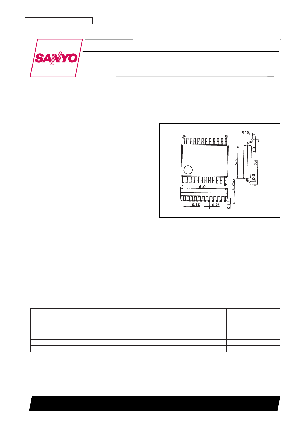
Package Dimensions
unit: mm
3175A-SSOP24
CMOS LSI
O3096HA(OT)/D3095HA (OT) No. 5159-1/16
SANYO: SSOP24
[LC74772V]
SANYO Electric Co.,Ltd. Semiconductor Bussiness Headquarters
TOKYO OFFICE Tokyo Bldg., 1-10, 1 Chome, Ueno, Taito-ku, TOKYO, 110 JAPAN
Camcorder On-Screen Display LSI
LC74772V
Ordering number : EN5159A
Parameter Symbol Conditions Ratings Unit
Supply voltage V
DD
V
DD
VSS– 0.3 to VSS+ 7.0 V
Input voltage V
IN
All input pins VSS– 0.3 to VDD+ 0.3 V
Output voltage V
OUT
CK
OUT
, CHA4, BLK4, CHA3, BLK3, B, G, R, BLANK VSS– 0.3 to VDD+ 0.3 V
Allowable power dissipation Pd max Ta = 25°C 300 mW
Operating temperature Topr –30 to +70 °C
Storage temperature Tstg –40 to +125 °C
Specifications
Absolute Maximum Ratings
Page 2
No. 5159-2/16
LC74772V
Parameter Symbol Conditions
Ratings
Unit
min typ max
Supply voltage V
DD
V
DD
2.7 5.0 5.5 V
Input high-level voltage V
IH
CTRL1, TESTIN, CS, SCLK, SIN, OUT
MOD
, HSYNC,
0.8 V
DD
VDD+ 0.3 V
VSYNC, RST
Input low-level voltage V
IL
CTRL1, TESTIN, CS, SCLK, SIN, OUT
MOD
, HSYNC,
V
SS
– 0.3 0.2 V
DD
V
VSYNC, RST
Oscillator frequency F
OSC
OSCIN, OSC
OUT
(LC oscillator) 6 (8) 10 MHz
Allowable Operating Ranges at Ta = –30 to +70°C
Parameter Symbol Conditions
Ratings
Unit
min typ max
CK
OUT
, CHA4, BLK4, CHA3, BLK3, B, G, R, BLANK:
Output high-level voltage V
OH
VDD= 5.5 to 4.5 V (VDD= 4.4 to 2.7 V), IOH= –1.0 mA 0.9 V
DD
V
(–0.5 mA)
CK
OUT
, CHA4, BLK4, CHA3, BLK3, B, G, R, BLANK:
Output low-level voltage V
OL
VDD= 5.5 to 4.5 V (VDD= 4.4 to 2.7 V), IOL= 1.0 mA 0.1 V
DD
V
(0.5 mA)
I
IH
CTRL1, TESTIN, CS, SCLK, SIN, OUT
MOD
, HSYNC,
1 µA
Input current
VSYNC: V
IN
= V
DD
I
IL
CTRL1, TESTIN, HSYNC, VSYNC: VIN= V
SS
–1 µA
Operating current drain I
DD
VDDpin; all outputs open, LC oscillator: 8 MHz 10 mA
Electrical Characteristics at Ta = –30 to +70°C, unless otherwise specified VDD= 5 V
Parameter Symbol Conditions
Ratings
Unit
min typ max
Minimum input pulse width
t
W (SCLK)
SCLK 200 ns
t
W (CS)
CS (the period that CS is high) 1 µs
Data setup time
t
SU (CS)
CS 200 ns
t
SU (SIN)
SIN 200 ns
Data hold time
t
h (CS)
CS 2 µs
t
h (SIN)
SIN 200 ns
One-word write time
t
word
The time to write 8 bits of data 4.2 µs
t
wt
The RAM data write time 1 µs
Timing Characteristics at Ta = –30 to +70°C, VDD= 5 ± 0.5 V
Page 3
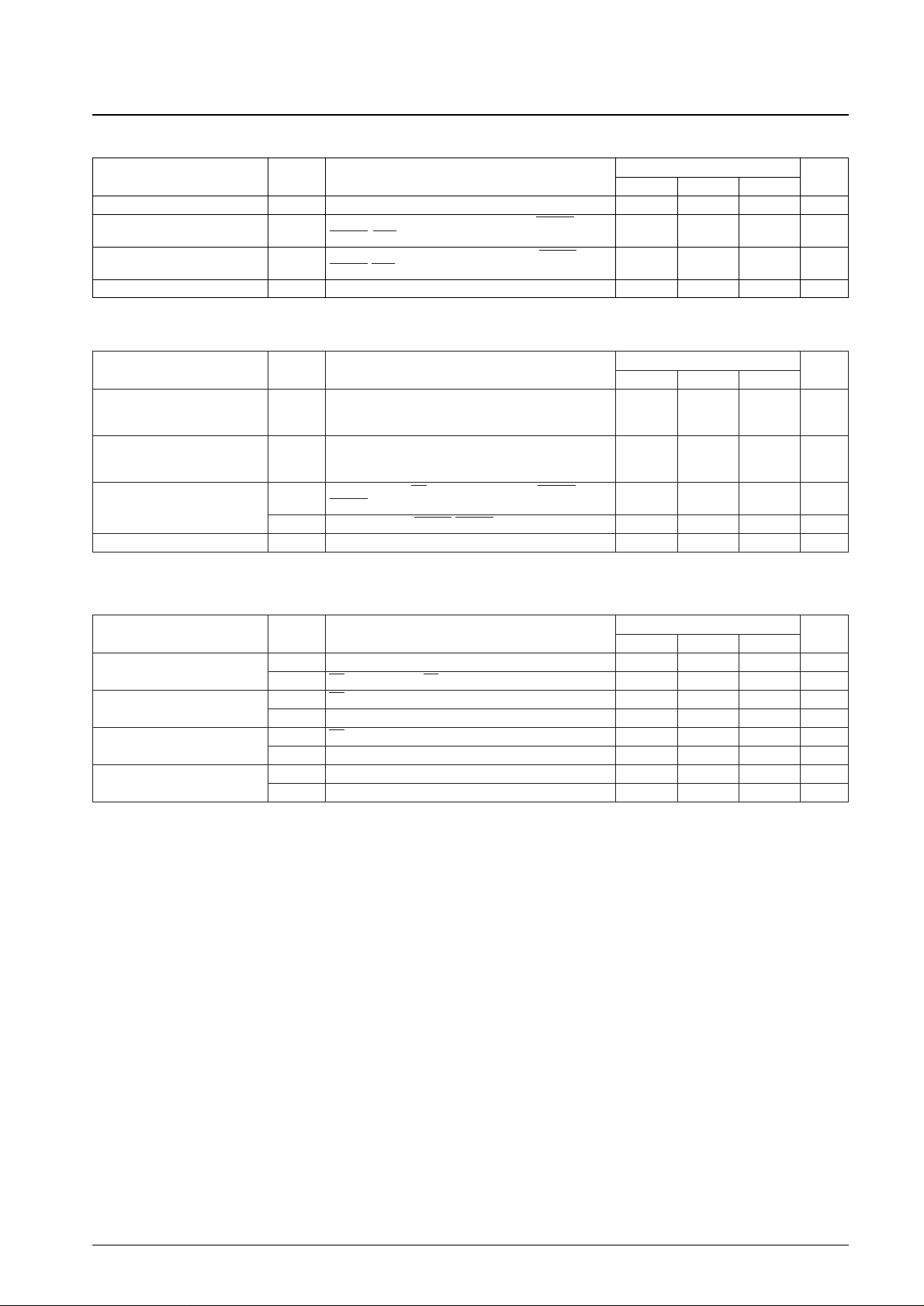
Serial Data Input Timing
Pin Assignment
The signal names in parentheses indicate the output pin functions when 4-system output mode is used.
No. 5159-3/16
LC74772V
Page 4
No. 5159-4/16
LC74772V
Pin Functions
PinNo. Symbol Function Description
1 V
SS
Ground Ground connection
2 OSC
IN
LC oscillator
Connections for the coil and capacitor that form the oscillator that generates the character
3 OSC
OUT
output horizontal dot clock.
4 CTRL1 Clock input control
Control input that switches between LC oscillator mode and clock input mode
Low: LC oscillator mode, high: clock input mode
5 TEST
IN
Test control input Test mode control input (The IC operates in test mode when this input is high.)
6 CS Enable input
Serial data input enable input
Low: active (This input has hysteresis characteristics.)
7 SCLK Clock input Serial data input clock input (This input has hysteresis characteristics.)
8 SIN Data input Serial data input (This input has hysteresis characteristics.)
9 CK
OUT
Clock output
LC oscillator clock monitor output
This signal is output when RST is low.
10 BLK4 Blanking signal output
Blanking signal output (system 2)
Functions as the system 4 blanking data signal output in 4-system mode.
11 CHA4 Character data output
Character data signal output (system 2)
Functions as the system 4 character data signal output in 4-system mode.
12 NC Unused Must be left open or tied to ground in normal operation.
13 NC Unused Must be left open or tied to ground in normal operation.
14 BLK3 Blanking signal output
Blanking signal output (system 1)
Functions as the system 3 blanking data signal output in 4-system mode.
15 CHA3 Character data output
Character data signal output (system 1)
Functions as the system 3 character data signal output in 4-system mode.
16 BLANK Blanking signal output
Blanking signal output (blanking signal for RGB output)
Functions as the system 2 blanking data signal output in 4-system mode.
17 R Character data output
Character data (R) signal output
Functions as the system 2 character data signal output in 4-system mode.
18 G Character data output
Character data (G) signal output
Functions as the system 1 blanking data signal output in 4-system mode.
19 B Character data output
Character data (B) signal output
Functions as the system 1 character data signal output in 4-system mode.
20 OUT
MOD
Output control input
Control input that switches between RGB output and 4-system output
Low: RGB output, high 4-system output
21 VSYNC
Vertical synchronizing
Vertical synchronizing signal input (This input has hysteresis characteristics.)
signal input
22 HSYNC Horizontal synchronizing
Horizontal synchronizing signal input (This input has hysteresis characteristics.)
signal input
23 RST Reset input System reset signal input (This input has hysteresis characteristics.)
24 V
DD
Power supply Power supply connection (+5 V)
Note: 1. Built-in pull-up resistors can be specified for inclusion in the CS (pin 6), SCLK (pin 7), SIN (pin 8), and RST (pin 23) pins as mask options.
2. In clock input mode (when CTRL1 is high), the function that holds the OSC
IN
(pin 2) pin high during an oscillator reset is stopped.
Page 5
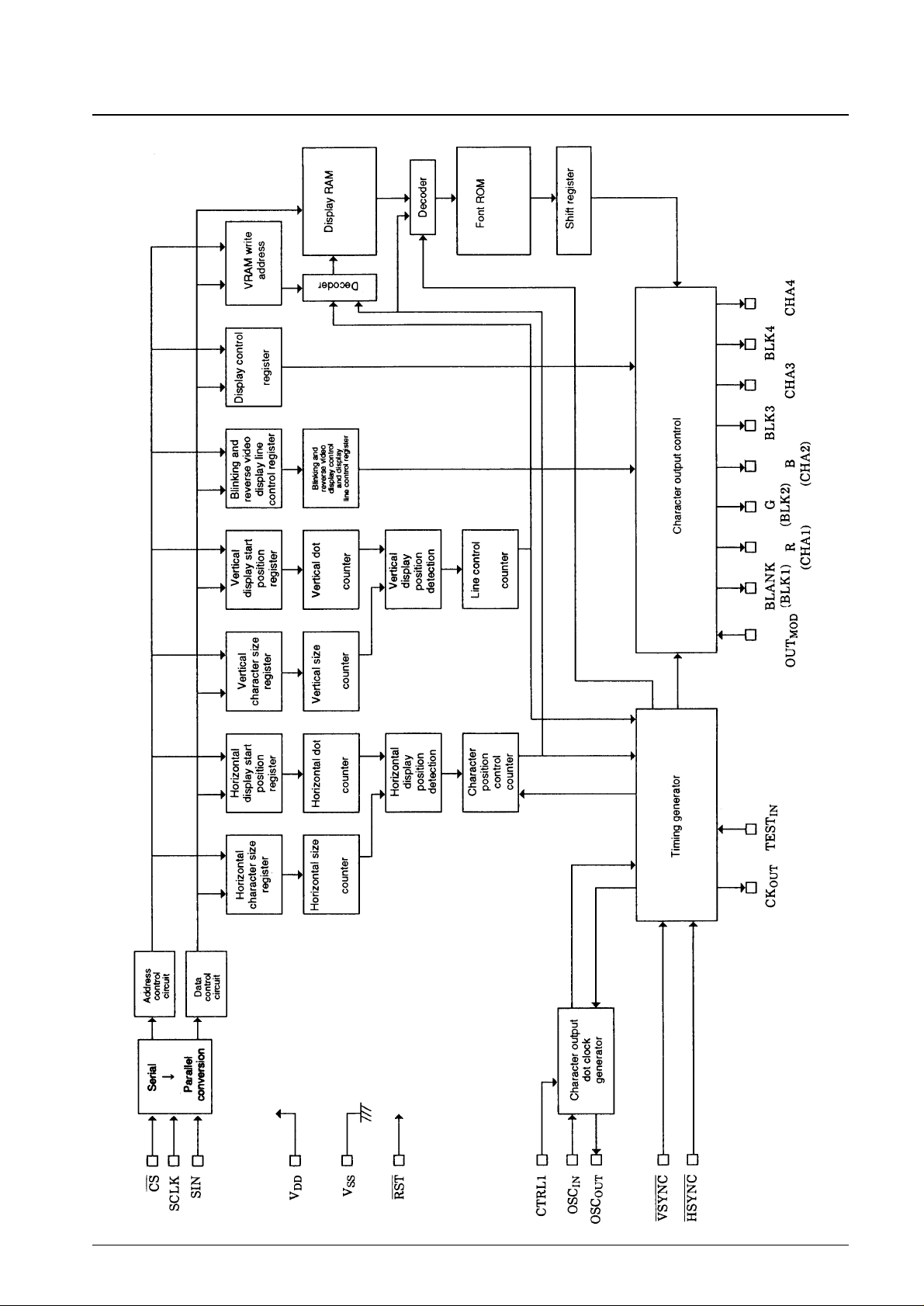
Block Diagram
No. 5159-5/16
LC74772V
Page 6

Display Control Commands
The display control commands have an 8-bit serial input format. Data is input LSB first.
Display Control Command Table
No. 5159-6/16
LC74772V
First byte Second byte
Command
Command code
Data Data
D7 D6 D5 D4 D3 D2 D1 D0 D7 D6 D5 D4 D3 D2 D1 D0
COMMAND 0
0 0 0 0
RST RAM OSC TST
— — — — — — — —
System setup 1 SYS CLR STP MOD
COMMAND 1
0 0 0 1
CSYN CLK CLK CLK
— — — — — — — —
System setup 2 MOD POLT MOD1 MOD0
COMMAND 2
0 0 1 0
VSYN HSYN DATA ART
— — — — — — — —
Input control setup POLT POLT FMT FMT
COMMAND 3
0 0 1 1
PORT OUT OUT OUT
— — — — — — — —
General-purpose port control SET P11 P10 P9
COMMAND 4
RVS BLK BLK BLK
Display operation control: 0 1 0 0
ON ON 1 0
— — — — — — — —
reverse video and blinking
COMMAND 5
DSP DSP DSP DSP
Display control: on/off settings 0 1 0 1
4 3 2 1
— — — — — — — —
for each output
COMMAND 6
0 1 1 0
DSPF DSP DSP DSP
— — — — — — — —
Output control: systems 3 and 4 SL34 RSG GSG BSG
COMMAND 8
1 0 0 0 0
BKC BKC BKC BKO4 BKO4 BKO3 BKO3 BKO2 BKO2 BKO1 BKO1
Display control: border R G B F1 F0 F1 F0 F1 F0 F1 F0
COMMAND 9
1 0 0 1 VP5 VP4 VP3 VP2 VP1 VP0 HP5 HP4 HP3 HP2 HP1 HP0
Display start position
COMMAND 10
1 0 1 0
LNF LNF LNF LN
0 0
LIN LIN LIN LIN LIN LIN
Display line control SZ OT4 OT3 SEL 126 115 104 93 82 71
COMMAND 11
1 0 1 1
VADR VADR VADR VADR
0 0 0
HADR HADR HADR HADR HADR
RAM write address 3 2 1 0 4 3 2 1 0
COMMAND 14
1 1 1 BLK RV R G B C7 C6 C5 C4 C3 C2 C1 C0
Display RAM setup data
① ②
①
Command code: (These 4 bits in the first byte identify the command.)
Command 14 is recognized by the upper 3 bits.
②
Command data: (These bits specify the data for each command.)
• For commands 0 through 7, 8 bits of data are read in.
• For commands 8 through 14, 16 bits of data are read in.
• If the command 1 data-9 bit (DATAFMT) was set to 1, after the first byte of a command 14 is read
in, the system goes to continuous transfer mode for reading in a series of following bytes.
Note: 1. If the CS pin is set high, the command state is set to the command 0 (system control setup) state.
2. If a system reset is executed from the RST pin or by a command reset, the command register is set tot 0.
Page 7

①
COMMAND 0 (System control setup 1)
First byte
Notes on command settings
1. RSTSYS: A command reset is executed immediately after the data is read.
The reset is cleared by returning the CS pin to high to reset this register. The reset is also cleared if this command is
executed consecutively or if this register is set to 0.
2. RAMCLR: The RAM can only be erased when display is off. This operation is not executed during display. This
operation cannot be executed if the LC oscillator is stopped. Only use this command when the LC oscillator is
operating.
• This command bit is automatically cleared when the RAM erase operation completes.
• Once the RAM erase command has been read in, the following time is required to complete the operation.
— Tclear = 5 [µs] + 4/f
OSC
(LC-oscillator) × 288
3. OSCSTP: The LC oscillator stop command stops the LC oscillator connected to pins 2 and 3 (OSCINand OSC
OUT
).
The oscillator stop command is only executed when display is off. It is not executed if display is in progress.
• In external clock input mode, this command stops the acquisition of that clock signal.
4. TSTMOD: The test mode command is executed if the TESTINpin (pin 5) is high. This command should not be used
by applications in normal operation.
Note: This register is set to 0 on a reset (either by the RST pin or by a command reset).
No. 5159-7/16
LC74772V
Register content
DA0 to DA7 Register name
State Function
Note
7 — 0
6 — 0
Command 0 identification code
5 — 0
4 — 0
3
RST
0 Normal operation
If CS is low, the reset is executed, but if
SYS
1 System reset
CS is high this command will be excluded.
RAM
0 Normal operation
The VRAM clear operation is not
2 executed when the oscillator
CLR
1 Normal operation VRAM clear (All data is set to FE (hexadecimal))
is stopped.
OSC
0 The LC oscillator operating state is maintained.
Valid when the display is off. VRAM write
1 is not possible when the oscillator is
STP
1 The LC oscillator is stopped.
stopped.
0
TST
0 Normal operation
Illegal setting.
MOD
1 Test mode
This bit must always be set to 0.
Page 8

②
COMMAND 1 (System control setup 2)
First byte
③
COMMAND 2 (Input control)
First byte
No. 5159-8/16
LC74772V
Register content
DA0 to DA7 Register name
State Function
Note
7 — 0
6 — 0
Command 1 identification code
5 — 0
4 — 1
0
HSYNC (pin 22) functions as the horizontal synchronizing
3
CSYN
signal input
MOD
1
HSYNC (pin 22) functions as the composite synchronizing
signal input
CLK
0 The system clock has a positive polarity.
2
POLT
1 The system clock has a negative polarity.
0
1
CLK
MOD1
1
0
0
CLK
MOD0
1
Valid when the CTRL1 pin (pin 4) is high.
The input clock frequency in clock input
mode is either 4fsc or the dot clock
frequency.
This sets the clock polarity for system
operation when pin 2 is used as a clock
input.
The VSYNC pin (pin 21) must be tied to
ground or V
DD
in composite
synchronizing signal input mode.
MOD1 MOD0 Operation
0 0 LC oscillator mode
0 1 Clock input (1 dot)
1 0 Clock input (NTSC)
1 1 Clock input (PAL)
Register content
DA0 to DA7 Register name
State Function
Note
7 — 0
6 — 0
Command 2 identification code
5 — 1
4 — 0
3
VSYN
0 The vertical synchronizing signal input polarity is low active.
Sets the pin 21 (VSYNC) signal input
POLT
1 The vertical synchronizing signal input polarity is high active.
polarity.
2
HSYN
0 The horizontal synchronizing signal input polarity is low active.
Sets the pin 22 (HSYNC) signal input
POLT
1 The horizontal synchronizing signal input polarity is high active.
polarity.
0 Data is transferred in 16-bit units.
1
DATA Sets the COMMAND 14 data transfer
FMT
1
Continuous transfers with the upper 8 bits input first and then
format.
the lower 8 bits
0
ATR
0 RV specifies the reverse video display function.
COMMAND-14 Data 11: Valid in RV
FMT
1 RV specifies system 3 output control.
RGB output mode.
Note: This register is set to 0 on a reset (either by the RST pin or by a command reset).
Page 9

No. 5159-9/16
LC74772V
④
COMMAND 3 (General-purpose port control)
First byte
⑤
COMMAND 4 (Display control: reverse video and blinking)
First byte
Note: This register is set to 0 on a reset (either by the RST pin or by a command reset).
Register content
DA0 to DA7 Register name
State Function
Note
7 — 0
6 — 0
Command 3 identification code
5 — 1
4 — 1
3
PORT
0 System 4 functions as a normal character and border outputs.
Controls the pin 10 (BLK4) and pin 11
SET
1 System 4 functions as general-purpose ports.
(CHA4) outputs.
2
OUT
0 The pin 11 output is set to low.
Sets the output when PORTSET is
P11
1 The pin 11 output is set to high.
set to 1.
1
OUT
0 The pin 10 output is set to low.
Sets the output when PORTSET is
P10
1 The pin 10 output is set to high.
set to 1.
0
OUT
0 The pin 9 output is set to low.
Sets the output for pin 9 during normal
P9
1 The pin 9 output is set to high.
operation (other than during a reset).
Register content
DA0 to DA7 Register name
State Function
Note
7 — 0
6 — 1
Command 4 identification code
5 — 0
4 — 0
0 —
3
RVS
ON
1
Characters for which the attribute is specified are displayed
in reverse video.
0 —
2
BLK
ON
1
Characters for which the attribute is specified are
displayed blinking.
0
1 BLK1
1
0
0 BLK0
1
The blinking period setting
The duty is 60% for all types.
Character display on: 60%
Character display off: 40%
V: Vertical period
BLK1 BLK0 Operation
0 0 V × 25 (PAL: 0.5 s)
0 1 V × 30 (NTSC: 0.5 s)
1 0 V × 50 (PAL: 1.0 s)
1 1 V × 60 (NTSC: 1.0 s)
Page 10

No. 5159-10/16
LC74772V
⑥
COMMAND 5 (Display control: on/off settings for each output system)
First byte
⑦
COMMAND 6 (Output control: systems 3 and 4 output control settings)
First byte
Register content
DA0 to DA7 Register name
State Function
Note
7 — 0
6 — 1
Command 5 identification code
5 — 0
4 — 1
3 DSP4
0 System 4 output off
Pin 10 (BLK4) and pin 11 (CHA4) output
1 System 4 output on
control
2 DSP3
0 System 3 output off
Pin 14 (BLK3) and pin 15 (CHA3) output
1 System 3 output on
control
0 System 2 output off
Pin 16 (BLK2) and pin 17 (CHA2) output
1 DSP2
control
1 System 2 output on Invalid in RGB output mode.
0 System 1 (RGB) output off
Pin 18 (BLK1) and pin 19 (CHA1) output
0 DSP1
control
1 System 1 (RGB) output on
Functions as the RGB output control in
RGB output mode.
Register content
DA0 to DA7 Register name
State Function
Note
7 — 0
6 — 1
Command 6 identification code
5 — 1
4 — 0
0
Sets the system 3 output conditions according to the command
3
DSPF
described below.
SL34
1
Sets the system 4 output conditions according to the command
described below.
0
2
DSP
RSG
1
0
1
DSP
GSG
1
0
0
DSP
BSG
1
Note: The following registers are set to
1 during a reset.
DSPRSG
DSPGSG
DSPBSG
As a result, the “All of R, G, B are
output” state is selected during a
reset.
Only system 4 is valid in 4-system
output mode. System 4 cannot be set
when the general-purpose output port
usage is specified.
DSPRSG DSPGSG DSPBSG Output selection
0 0 0
Signals other than R, G,
B are output.
0 0 1 B is output.
0 1 0 G is output.
0 1 1 G and B are output.
1 0 0 R is output.
1 0 1 R and B are output.
1 1 0 R and G are output.
1 1 1 All of R, G, B are output.
Note: This register is set to 0 on a reset (either by the RST pin or by a command reset).
Page 11

No. 5159-11/16
LC74772V
⑧
COMMAND 8 (Output control: background color setting: RGB output mode)
First byte
Second byte
Register content
DA0 to DA7 Register name
State Function
Note
7 — 1
6 — 0
Command 8 identification code
5 — 0
4 — 0
3 0 —
0
2 BKCR
1
0
1 BKCG
1
0
0 BKCB
1
Background color setting in RGB output
mode
This command is invalid in 4-system
output mode.
• Invalid when pin 20 (OUT
MOD
) is high.
• Valid when pin 20 (OUT
MOD
) is low.
BKCR BKCG BKCB Background color
0 0 0 Black
0 0 1 Blue
0 1 0 Green
0 1 1 Cyan
1 0 0 Red
1 0 1 Magenta
1 1 0 Yellow
1 1 1 White
Register content
DA0 to DA7 Register name
State Function
Note
0
7
BKO4
F1
1
0
6
BKO4
F0
1
0
5
BKO3
F1
1
0
4
BKO3
F0
1
0
3
BKO2
F1
1
0
2
BKO2
F0
1
0
1
BKO1
F1
1
0
0
BKO1
F0
1
The system 1 or RGB output border
setting
The system 2 output border setting
This command is invalid in RGB output
mode.
• Invalid when pin 20 (OUT
MOD
) is low.
• Valid when pin 20 (OUT
MOD
) is high.
The system 3 output border setting
The system 4 output border setting
BKO4F1 BKO4F0 Operation function
0 0 No background or border
0 1 Font size (black characters)
1 0 Border
1 1 Areas other than the font (all filled)
BKO3F1 BKO3F0 Operation function
0 0 No background or border
0 1 Font size (black characters)
1 0 Border
1 1 Areas other than the font (all filled)
BKO2F1 BKO2F0 Operation function
0 0 No background or border
0 1 Font size (black characters)
1 0 Border
1 1 Areas other than the font (all filled)
BKO1F1 BKO1F0 Operation function
0 0 No background or border
0 1 Font size
1 0 Border
1 1 Areas other than the font (all filled)
Note: This register is set to 0 on a reset (either by the RST pin or by a command reset).
Page 12

No. 5159-12/16
LC74772V
⑨
COMMAND 9 (Display start position setting)
First byte
Second byte
Register content
DA0 to DA7 Register name
State Function
Note
7 — 1
6 — 0
Command 9 identification code
5 — 0
4 — 1
0
3 VP5
1
0
2 VP4
1
0
1 VP3
1
0
0 VP2
1
If VS is the vertical display start position then:
5
VS = H × (Σ 2nVPn) + 16H
n = 0
Where H is horizontal period pulse period.
Register content
DA0 to DA7 Register name
State Function
Note
7 VP1
0
1
6 VP0
0
1
5 HP5
0
1
4 HP4
0
1
3 HP3
0
1
2 HP2
0
1
1 HP1
0
1
0 HP0
0
1
If VS is the horizontal display start position then:
5
HS = Tc × (Σ 2nHPn) + 12Tc
n = 0
Where Tc is a single period of the LC oscillator connected to pins
2 and 3 (OSC
IN
and OSC
OUT
), or:
Tc is the period of the input clock (4fsc input) if CTRL1 (pin 4) is
high.
NTSC mode: 7.159 MHz = 4fsc × 1/2
PAL mode: 7.094 MHz = 4fsc × 2/5
Note: This register is set to 0 on a reset (either by the RST pin or by a command reset).
Page 13

No. 5159-13/16
LC74772V
⑩
COMMAND 10 (Display line control)
First byte
Second byte
Note: This register is set to 0 on a reset (either by the RST pin or by a command reset).
Register content
DA0 to DA7 Register name
State Function
Note
7 — 1
6 — 0
Command 10 identification code
5 — 1
4 — 0
3
LNF
0 —
SZ
1 Sets the character size.
2
LNF
0 —
Invalid in general-purpose port mode.
OT4
1 Sets the system 4 display line.
1
LNF
0 —
Invalid in system 4 output setup mode.
OT3
1 Sets the system 3 display line.
0
LNF
0 The line specified by the next 6 bits is one of lines 1 to 6.
Controls the line switching specified by
SEL
1 The line specified by the next 6 bits is one of lines 7 to 12.
the six bits in the second byte.
Register content
DA0 to DA7 Register name
State Function
Note
7 — 0 —
6 — 0 —
5
LIN
0 Clears the line 6 (12) setting.
126
1 Sets line 6 (12).
4
LIN
0 Clears the line 5 (11) setting.
115
1 Sets line 5 (11).
3
LIN
0 Clears the line 4 (10) setting.
104
1 Sets line 4 (10).
2
LIN
0 Clears the line 3 (9) setting.
93
1 Sets line 3 (9).
1
LIN
0 Clears the line 2 (8) setting.
82
1 Sets line 2 (8).
0
LIN
0 Clears the line 1 (7) setting.
71
1 Sets line 1 (7).
The character size or display line
setting
0: Character size specification = normal
Display line specification = off
1: Character size specification = double
size
Display line specification = on
Page 14

No. 5159-14/16
LC74772V
11 COMMAND 11 (Display RAM write address setting)
First byte
Second byte
Note: This register is set to 0 on a reset (either by the RST pin or by a command reset).
Register content
DA0 to DA7 Register name
State Function
Note
7 — 1
6 — 0
Command 11 identification code
5 — 1
4 — 1
3
VADR
0
3
1
2
VADR
0
2
1
1
VADR
0
1
1
0
VADR
0
0
1
The range of the display RAM vertical address (line address)
setting is from 0 to B (hexadecimal) (12 lines).
Values of C (hexadecimal) or larger are not allowed.
Register content
DA0 to DA7 Register name
State Function
Note
7 — 0 —
6 — 0 —
5 — 0 —
4
HADR
0
4
1
3
HADR
0
3
1
2
HADR
0
2
1
1
HADR
0
1
1
0
HADR
0
0
1
The range of the display RAM horizontal address (character
address) setting is from 00 to 17 (hexadecimal) (24 characters).
Values of 18 (hexadecimal) or larger are not allowed.
Page 15

No. 5159-15/16
LC74772V
Second byte
Note: This register is set to 0 on a reset (either by the RST pin or by a command reset).
12 COMMAND 14 (Display RAM setup data)
First byte
Register content
DA0 to DA7 Register name
State Function
Note
7 C7
0
1
6 C6
0
1
5 C5
0
1
4 C4
0
1
3 C3
0
1
2 C2
0
1
1 C1
0
1
0 C0
0
1
Character code setting
There are 256 characters (00 to FF hexadecimal).
FE hexadecimal is handled as blank data.
Nothing is displayed, whatever the other conditions are set to.
FF hexadecimal functions as the transfer termination code for
character-code-only continuous transfers.
Continuous transfer mode is set up by setting the data 0 bit
(DATAFMT) in COMMAND 2 to 1.
Register content
DA0 to DA7 Register name
State Function
Note
7 — 1
6 — 1 Command 14 identification code
5 — 1
4 BLK
0 —
1 Blinking character specification
3 RV
0 —
1 Reverse video character specification
2 R
0 —
1 R output specification (system 3 output in 4-system output mode)
1 G
0 —
1 G output specification (system 2 output in 4-system output mode)
0 B
0 —
1 B output specification (system 1 output in 4-system output mode)
Page 16

No. 5159-16/16
LC74772V
Display Screen Organization
The display screen consists of 12 lines of 24 characters each.
Thus the maximum number of characters that can be displayed is 288 characters.
The display memory address consists of a line address (VADR0, VADR1, VADR2, and VADR3 representing values
from 0 to B (hexadecimal)), and a column (character position) address (HADR0, HADR1, HADR2, HADR3, and
HADR4 representing values from 0 to 17 (hexadecimal)).
Display Screen Organization (Display memory address)
This catalog provides information as of August, 1997. Specifications and information herein are subject to
change without notice.
■ No products described or contained herein are intended for use in surgical implants, life-support systems, aerospace
equipment, nuclear power control systems, vehicles, disaster/crime-prevention equipment and the like, the failure of
which may directly or indirectly cause injury, death or property loss.
■ Anyone purchasing any products described or contained herein for an above-mentioned use shall:
➀ Accept full responsibility and indemnify and defend SANYO ELECTRIC CO., LTD., its affiliates, subsidiaries and
distributors and all their officers and employees, jointly and severally, against any and all claims and litigation and all
damages, cost and expenses associated with such use:
➁ Not impose any responsibility for any fault or negligence which may be cited in any such claim or litigation on
SANYO ELECTRIC CO., LTD., its affiliates, subsidiaries and distributors or any of their officers and employees
jointly or severally.
■ Information (including circuit diagrams and circuit parameters) herein is for example only; it is not guaranteed for
volume production. SANYO believes information herein is accurate and reliable, but no guarantees are made or implied
regarding its use or any infringements of intellectual property rights or other rights of third parties.
 Loading...