

Page 1
Ordering number : EN4248A
31596HA (OT) No. 4248-1/11
Overview
The LC74770M is a CMOS LSI that implements onscreen display, a function that displays characters and
patterns on display screens such as camcorder viewfinder
screens under microprocessor control. This LSI displays
12-dot by 18-dot characters.
Features
• Display format: 24 characters by 12 rows (up to
288 characters)
• Characters displayed: Up to 288 characters
• Character format: 12 (horizontal) × 18 (vertical)
• Characters in font: 128
• Character sizes: Normal and double
• Initial display positions: 64 horizontal positions and
64 vertical positions
• Reverse video function: Characters can be displayed in
reverse video specified in units of individual characters.
• Blinking types: In character units in one of two periods,
1.0 second and 0.5 second, with a 50% duty.
• Outputs: Character and blanking data, with two output
systems for each
• External control input: 8-bit serial input format
• General-purpose output port: 4 bits (controlled from the
serial input data)
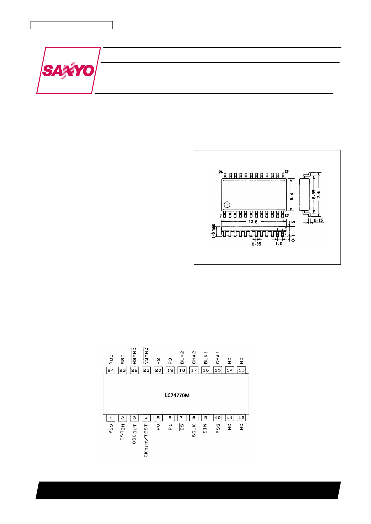
Pin Assignment
Package Dimensions
unit: mm
3112-MFP24S
SANYO: MFP24S
[LC74770M]
LC74770M
SANYO Electric Co.,Ltd. Semiconductor Bussiness Headquarters
TOKYO OFFICE Tokyo Bldg., 1-10, 1 Chome, Ueno, Taito-ku, TOKYO, 110-0005 JAPAN
On-Screen Display Controller LSI
CMOS LSI
Top view
Page 2
Specifications
Absolute Maximum Ratings at Ta = 25°C
Allowable Operating Ranges at Ta = –30 to +70°C
Electrical Characteristics at Ta = –30 to +70°C, VDD= 5 V unless otherwise specified.
Timing Characteristics at Ta = –30 to +70°C, VDD= 5 ± 0.5 V
No. 4248-2/11
LC74770M
Parameter Symbol Conditions Ratings Unit
Maximum supply voltage V
DD
max V
DD
VSS– 0.3 to VSS+ 7.0 V
Maximum input voltage V
IN
max All input pins VSS– 0.3 to VDD+ 0.3 V
Maximum output voltage V
OUT
max BLK1, BLK2, CHA1, CHA2, P0 to P3, CK
OUT
VSS– 0.3 to VDD+ 0.3 V
Allowable power dissipation Pd max 300 mW
Operating temperature Topr –30 to +70 °C
Storage temperature Tstg –40 to +125 °C
Parameter Symbol Conditions min typ max Unit
Supply voltage V
DD
V
DD
4.5 5.0 5.5 V
Input high-level voltage V
IH
RST, CS, SIN, SCLK, HSYNC, VSYNC 0.8 V
DD
VDD+ 0.3 V
Input low-level voltage V
IL
RST, CS, SIN, SCLK, HSYNC, VSYNC VSS– 0.3 0.2 V
DD
V
Oscillator frequency f
OSC
OSCINand OSC
OUT
oscillator pins 5 7 10 MHz
Parameter Symbol Conditions min typ max Unit
Output high-level voltage V
OH
BLK1, BLK2, CHA1, CHA2, P0 to P3: VDD= 5.0 V,
4.5 V
I
OH
= –1.0 mA
Output low-level voltage V
OL
BLK1, BLK2, CHA1, CHA2, P0 to P3: VDD= 5.0 V,
0.5 V
I
OL
= 1.0 mA
Input current
I
IH
RST, CS, SIN, SCLK, HSYNC, VSYNC: VIN= V
DD
1 µA
I
IL
HSYNC, VSYNC: VIN= V
SS
–1 µA
Operating current drain I
DD
VDD: all outputs open, LC = 7 MHz 10 mA
Parameter Symbol Conditions min typ max Unit
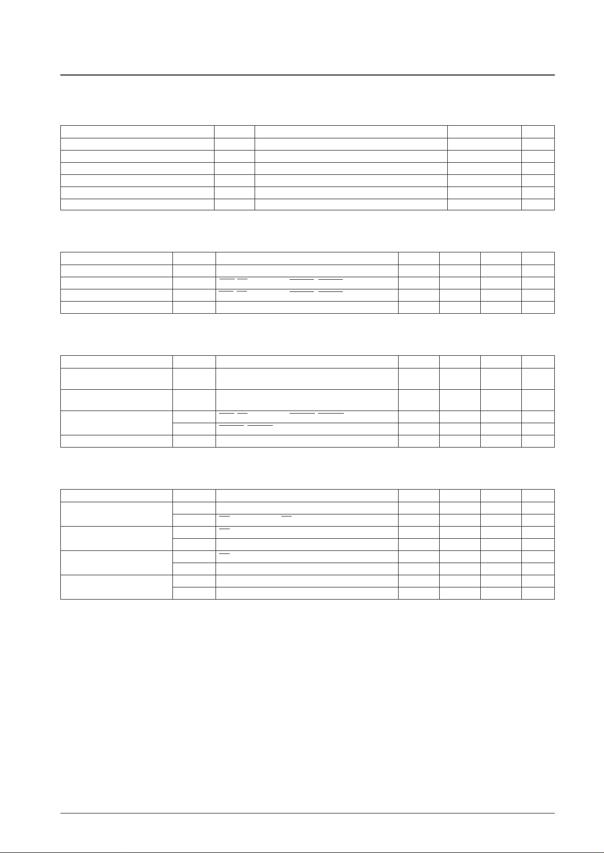
Minimum input pulse width
t
W (SCLK)
SCLK 200 ns
t
W (CS)
CS (the period that CS is high) 1 µs
Data setup time
t
SU (CS)
CS 200 ns
t
SU (SIN)
SIN 200 ns
Data hold time
t
h (CS)
CS 2 µs
t
h (SIN)
SIN 200 ns
Single word write time
t
word
The time to write 8 bits of data 4.2 µs
t
wt
The time to write RAM data 1 µs
Page 3
Serial Data Input Timing
Pin Functions
No. 4248-3/11
LC74770M
No. Symbol Pin Function
1 V
SS
Ground pin Ground connection
2 OSC
IN
LC oscillator pin
Connections for the coil and capacitor that form the oscillator that generates the character output
3 OSC
OUT
dot clock.
4 CK
OUT
/TEST
Clock output/test
Provides the OSC
OUT
output (when RST is low) and the test mode output.
output pin
5 P0
General-purpose port 0
General-purpose port (PORT0) output
output pin
6 P1
General-purpose port 1
General-purpose port (PORT1) output
output pin
7 CS Enable input pin
Enable input for the serial data input function. Serial data input is enabled when this pin is low.
A pull-up resistor is built in, i.e., this is a hysteresis input.
8 SCLK Clock input pin
Clock input for the serial data input function. A pull-up resistor is built in,
i.e., this is a hysteresis input.
9 SIN Data input pin Serial data input. A pull-up resistor is built in, i.e., this is a hysteresis input.
10 V
SS
Ground pin Ground connection
11 NC No connection
12 NC No connection
Unused pins.
13 NC No connection
These pins must be left open or connected to ground.
14 NC No connection
15 CHA1 Character 1 output pin System 1 character data output
16 BLK1 Blank 1 output pin System 1 blank data output
17 CHA2 Character 2 output pin System 2 character data output
18 BLK2 Blank 2 output pin System 2 blank data output
19 P3
General-purpose port 3
General-purpose port (PORT3) output
output pin
20 P2
General-purpose port 2
General-purpose port (PORT2) output
output pin
21 VSYNC
Vertical synchronizing
Input for the vertical synchronizing signal (active low)
signal input pin
22 HSYNC
Horizontal synchronizing
Input for the horizontal synchronizing signal (active low)
signal input pin
23 RST Reset input pin System reset input (active low) A pull-up resistor is built in, i.e., this is a hysteresis input.
24 V
DD
Power supply pin (+5 V) Power supply (+5 V)
Page 4
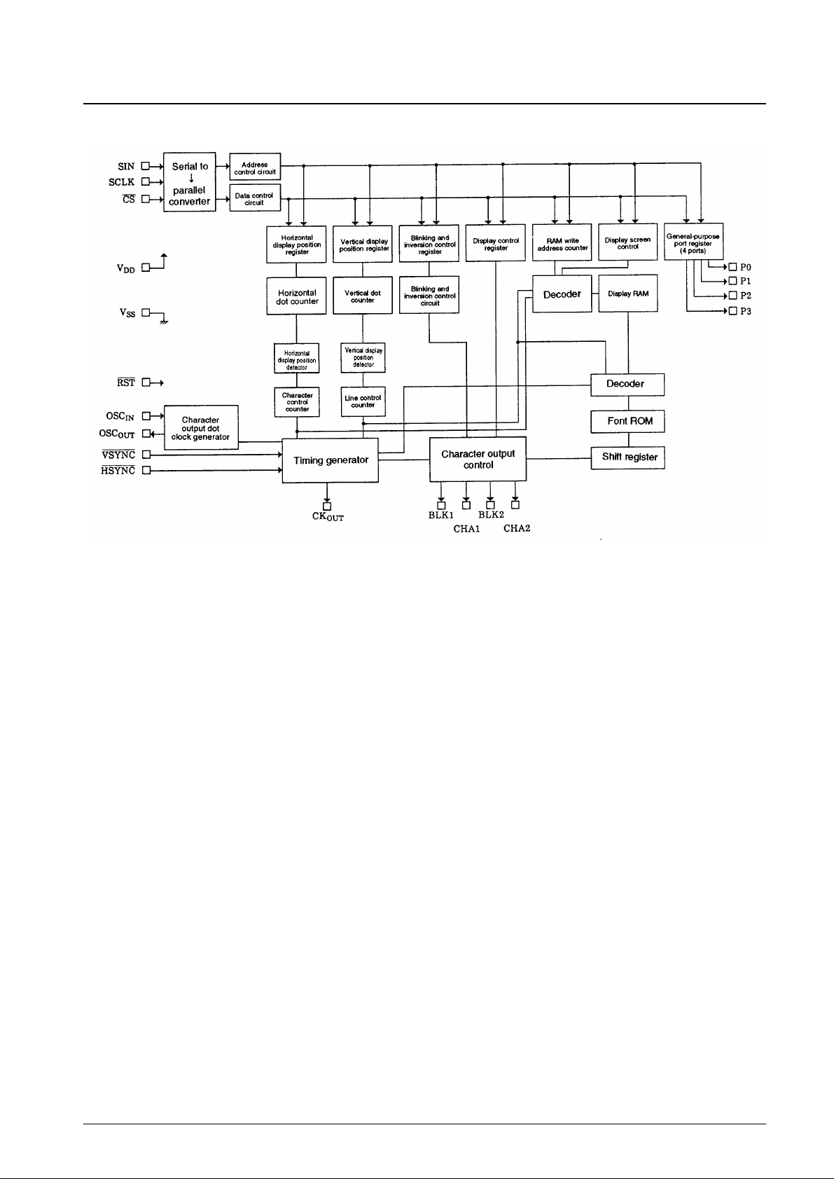
Block Diagram
Display Control Commands
Display control commands have an 8-bit format and are transferred using the serial input function. Commands consist of
a command identification code in the first byte and command data in the following bytes. The following commands are
supported.
1 COMMAND 0: Display memory (VRAM) write address setup command
2 COMMAND 1: Display character data write command
3 COMMAND 2: Vertical display start position and vertical character size setup command
4 COMMAND 3: Horizontal display start position and horizontal character size setup command
5 COMMAND 4: Display control setup command
6 COMMAND 5: System 2 (BLK2 and CHA2) output control (lines 1 to 6) and line size setting command
7 COMMAND 6: System 2 (BLK2 and CHA2) output control (lines 7 to 12) and general-purpose port setting command
No. 4248-4/11
LC74770M
Page 5

Display Control Command Table
Once written, the command identification code in the first byte is stored until the next first byte is written. However,
when the display character data write command (COMMAND1) is written, the LC74770M locks into the display
character data write mode, and another first byte cannot be written.
When a high level is input to the CS pin, the LC74770M is set to COMMAND0 (display memory write address setup
mode).
1 COMMAND 0 (Display memory write address setup command)
First byte
No. 4248-5/11
LC74770M
First byte Second byte
Command
Command identification code
Data Data
7 6 5 4 3 2 1 0 7 6 5 4 3 2 1 0
COMMAND 0 1 0 0 0 V3 V2 V1 V0 0 0 0 H4 H3 H2 H1 H0
Write address
COMMAND 1 1 0 0 1 0 0 0 0 at c6 c5 c4 c3 c2 c1 c0
Character write
COMMAND 2
1 0 1 0 0 0 0 0 0 0 VP VP VP VP VP VP
Vertical display position
5 4 3 2 1 0
start position
COMMAND 3
1 0 1 1 0 0 0 0 0 0 HP HP HP HP HP HP
Horizontal display position
5 4 3 2 1 0
start position
COMMAND 4 1 1 0 0 TST RCL OSC RST 0 MD1 MD0 EG BK BK RV DSP
Display control 1 0
COMMAND 5
1 1 0 1 0 0 0 LS 0 0 LN LN LN LN LN LN
BLK2 and CHA2 output control:
6 5 4 3 2 1
lines 1 to 6, and line size control
COMMAND 6
BLK2 and CHA2 output control: 1 1 1 0 P3 P2 P1 P0 0 0 LN LN LN LN LN LN
lines 7 to 12, and general-purpose 12 11 10 9 8 7
port control
Register content
DA0 to DA7 Register name
State Function
Note
7 — 1
6 — 0
Command 0 identification code
5 — 0 Sets the display memory write address.
4 — 0
3 V3
0
1
2 V2
0
1
Display memory address (0 to B hexadecimal)
1 V1
0
1
0 V0
0
1
Page 6

Second byte
Note: All registers are set to 0 when the LC74770M is reset by the RST pin.
2 COMMAND 1 (Display character data write setup command)
First byte
Second byte
Note: All registers are set to 0 when the LC74770M is reset by the RST pin.
No. 4248-6/11
LC74770M
Register content
DA0 to DA7 Register name
State Function
Note
7 — 0 Second byte identification bit
6 — 0
5 — 0
4 H4
0
1
3 H3
0
1
2 H2
0
Display memory address (0 to 17 hexadecimal)
1
1 H1
0
1
0 H0
0
1
Register content
DA0 to DA7 Register name
State Function
Note
7 — 1
6 — 0
Command 1 identification code
5 — 0
Sets up display character data write.
4 — 1
3 — 0
2 — 0
1 — 0
0 — 0
When this command is input, the
LC74770M locks into the display
character data write mode until the CS
pin goes high.
Register content
DA0 to DA7 Register name
State Function
Note
7 at
0 Character attribute off
1 Character attribute on
6 c6
0
1
5 c5
0
1
4 c4
0
1
3 c3
0
Character code (00 to 7F hexadecimal)
1
2 c2
0
1
1 c1
0
1
0 c0
0
1
Page 7

3 COMMAND 2 (Vertical display start position setup command)
First byte
Second byte
Note: All registers are set to 0 when the LC74770M is reset by the RST pin.
4 COMMAND 3 (Horizontal display start position setup command)
First byte
No. 4248-7/11
LC74770M
Register content
DA0 to DA7 Register name
State Function
Note
7 — 1
6 — 0
Command 2 identification code
5 — 1
Sets the vertical display start position.
4 — 0
3 — 0
2 — 0
1 — 0
0 — 0
Register content
DA0 to DA7 Register name
State Function
Note
7 — 1
6 — 0
Command 3 identification code
5 — 1
Sets the horizontal display start position.
4 — 1
3 — 0
2 — 0
1 — 0
0 — 0
Register content
DA0 to DA7 Register name
State Function
Note
7 — 0 Second byte identification bit
6 — 0
5
VP5
0
(MSB)
1
4 VP4
0
1
3 VP3
0
1
2 VP2
0
1
1 VP1
0
1
0
VP0
0
(LSB)
1
The vertical display start position is set
by the 6 bits VP0 to VP5.
The weight of bit 1 is 1H.
If VS is the vertical display start position then:
5
VS = H × (Σ 2nVPn)
n = 0
H: the horizontal synchronization pulse period
Page 8

Second byte
Note: All registers are set to 0 when the LC74770M is reset by the RST pin.
5 COMMAND 4 (Display control setup command)
First byte
No. 4248-8/11
LC74770M
Register content
DA0 to DA7 Register name
State Function
Note
7 — 0 Second byte identification bit
6 — 0
5
HP5
0
(MSB)
1
4 HP4
0
1
3 HP3
0
1
2 HP2
0
1
1 HP1
0
1
0
HP0
0
(LSB)
1
The horizontal display start position is
set by the 6 bits HP0 to HP5.
The weight of bit 1 is 1Tc.
If HS is the horizontal start position then:
5
HS = Tc × (Σ 2nHPn)
n = 0
Tc: Period of the oscillator connected to OSCIN/OSC
OUT
in
operating mode.
Register content
DA0 to DA7 Register name
State Function
Note
7 — 1
6 — 1
Command 4 identification code
5 — 0 Sets up display control.
4 — 0
3
TST
0 Normal operating mode
This bit must be zero.
(TSTMOD)
1 Test mode
2
RCL
0
Valid when display is off.
(RAMCLR)
1 Erase display RAM (Data is set to 7F hexadecimal.)
1
OSC
0 Do not stop the LC oscillator circuit.
This bit must be zero.
(OSCSTP)
1 Stop the LC oscillator circuit.
RST
0
The LSI is reset when the CS pin is low,
0
(SYSRST)
and the reset is cleared when that pin
1 Reset all registers and turn the display off.
goes high.
Page 9

Second byte
Note: All registers are set to 0 when the LC74770M is reset by the RST pin.
6 COMMAND 5 (System 2 output control and line size setting command)
First byte
Second byte
Note: All registers are set to 0 when the LC74770M is reset by the RST pin.
No. 4248-9/11
LC74770M
Register content
DA0 to DA7 Register name
State Function
Note
7 — 0 Second byte identification bit
6 MD1
0 The blank output also outputs character data.
Blank output control
1 The blank output only outputs blank data.
5 MD0
0 The system 1 output outputs all lines.
Output system 1 control
1 The system 1 output only outputs lines not output by system 2.
4 EG
0 Border off
1 Border on
3 BK1
0 Blinking period set to about 0.5 second.
Blinking period switching
1 Blinking period set to about 1 second.
0 Blinking off
Blinking of reverse video characters
2 BK0 consists of alternation between normal
1 Blinking on
and reverse video.
1 RV
0 Reverse video off
1 Reverse video on
0
DSP
0 Character display off
(DSPON)
1 Character display on
Register content
DA0 to DA7 Register name
State Function
Note
7 — 1
Command 5 identification code
6 — 1
Controls output system 2 and sets the line size.
5 — 0
(Output control for CHA2 and BLK2)
4 — 1
(Line size control)
3 — 0
2 — 0
1 — 0
0 LS
0 Output line selection
The line is selected in the second byte.
1 Character size selection (line units)
Register content
DA0 to DA7 Register name
State Function
Note
7 — 0 Second byte identification bit
6 — 0
5 LN6
0 The sixth line of data is not output to CHA2 and BLK2.
1 The sixth line of data is output to CHA2 and BLK2.
4 LN5
0 The fifth line of data is not output to CHA2 and BLK2.
1 The fifth line of data is output to CHA2 and BLK2.
3 LN4
0 The fourth line of data is not output to CHA2 and BLK2.
1 The fourth line of data is output to CHA2 and BLK2.
2 LN3
0 The third line of data is not output to CHA2 and BLK2.
1 The third line of data is output to CHA2 and BLK2.
1 LN2
0 The second line of data is not output to CHA2 and BLK2.
1 The second line of data is output to CHA2 and BLK2.
0 LN1
0 The first line of data is not output to CHA2 and BLK2.
1 The first line of data is output to CHA2 and BLK2.
Used for the line output setting when LS
is low.
Used for the line size setting when LS is
high.
Note:
LS = 1: Set the line size.
LS = 0: Specifies line output.
Page 10

7 COMMAND 6 (System 2 output control and general-purpose port setting command)
First byte
Second byte
Note: All registers are set to 0 when the LC74770M is reset by the RST pin.
No. 4248-10/11
LC74770M
Register content
DA0 to DA7 Register name
State Function
Note
7 — 0 Second byte identification bit
6 — 0
5 LN12
0 The twelfth line of data is not output to CHA2 and BLK2.
1 The twelfth line of data is output to CHA2 and BLK2.
4 LN11
0 The eleventh line of data is not output to CHA2 and BLK2.
1 The eleventh line of data is output to CHA2 and BLK2.
3 LN10
0 The tenth line of data is not output to CHA2 and BLK2.
1 The tenth line of data is output to CHA2 and BLK2.
2 LN9
0 The ninth line of data is not output to CHA2 and BLK2.
1 The ninth line of data is output to CHA2 and BLK2.
1 LN8
0 The eighth line of data is not output to CHA2 and BLK2.
1 The eighth line of data is output to CHA2 and BLK2.
0 LN7
0 The seventh line of data is not output to CHA2 and BLK2.
1 The seventh line of data is output to CHA2 and BLK2.
Register content
DA0 to DA7 Register name
State Function
Note
7 — 1
Command 6 identification code
6 — 1
Controls output system 2 output.
5 — 1
(Output control for CHA2 and BLK2)
4 — 0
(General-purpose port output control)
3 P3
0 Sets the general-purpose port output (P3) to low.
1 Sets the general-purpose port output (P3) to high.
2 P2
0 Sets the general-purpose port output (P2) to low.
1 Sets the general-purpose port output (P2) to high.
1 P1
0 Sets the general-purpose port output (P1) to low.
1 Sets the general-purpose port output (P1) to high.
0 P0
0 Sets the general-purpose port output (P0) to low.
1 Sets the general-purpose port output (P0) to high.
Used for the line output setting when LS
is low.
Used for the line size setting when LS is
high.
Note:
LS = 1: Set the line size.
LS = 0: Specifies line output.
Page 11

PS No. 4248-11/11
LC74770M
Display Screen Structure
The display consists of 12 lines of 24 characters each and thus up to 288 characters can be displayed.
Display memory addresses are specified as row (0 to B hexadecimal) and column (0 to 17 hexadecimal) addresses.
Display Screen Structure (display memory addresses)
This catalog provides information as of March, 1996. Specifications and information herein are subject to
change without notice.
■ No products described or contained herein are intended for use in surgical implants, life-support systems, aerospace
equipment, nuclear power control systems, vehicles, disaster/crime-prevention equipment and the like, the failure of
which may directly or indirectly cause injury, death or property loss.
■ Anyone purchasing any products described or contained herein for an above-mentioned use shall:
➀ Accept full responsibility and indemnify and defend SANYO ELECTRIC CO., LTD., its affiliates, subsidiaries and
distributors and all their officers and employees, jointly and severally, against any and all claims and litigation and all
damages, cost and expenses associated with such use:
➁ Not impose any responsibility for any fault or negligence which may be cited in any such claim or litigation on
SANYO ELECTRIC CO., LTD., its affiliates, subsidiaries and distributors or any of their officers and employees
jointly or severally.
■ Information (including circuit diagrams and circuit parameters) herein is for example only; it is not guaranteed for
volume production. SANYO believes information herein is accurate and reliable, but no guarantees are made or implied
regarding its use or any infringements of intellectual property rights or other rights of third parties.
 Loading...