

Page 1
Overview
The LC74751 is a CMOS LSI that supports on-screen
display of characters and patterns on a TV screen under
the control of a microcontroller. The LC74751 includes an
on-chip character ROM that provides 128 characters in a
12 × 18 dot format. This IC supports display of up to 12
lines of 24 characters each for a maximum of 288
characters.
Features
• Display format: 24 characters by 12 rows
• Characters displayed: Up to 288 characters
• Display control ROM (line ROM): ROM for 64 lines
(Control in line units: lines consisting of 24 characters)
• Display RAM: 176 characters (Used for the specification
of user-defined characters.)
• Character format: 12 (horizontal) × 18 (vertical) dots
• Characters in font: 128
• Character sizes: Four sizes each in the horizontal and
vertical directions
• Initial display positions: 64 horizontal positions and 64
vertical positions
• Blinking: Specifiable in character units
• Blinking types:
— Two periods supported: 1.0 second and 0.5 second
— Three duty types supported: 25%, 50%, and 75%
• Blanking: Over the whole font (12 × 18 dots)
• Background color
— 8 background colors (in internal synchronization
mode): 4fsc (NTSC/PAL/PAL-M/PAL-N)
— 4 background colors (in internal synchronization
mode): 2fsc (NTSC)
— Single background color (blue) (in internal
synchronization mode): 2fsc (PAL/PAL-M/PAL-N)
• External control input: Serial data input
• Synchronizing signals: Supports switching between
internal and external synchronizing signals.
• On-chip sync separator circuit
• Video output: Composite video output in the NTSC,
PAL, PAL-M, or PAL-N format
• Superimpose function: Superimposes the character
output on the composite video output.
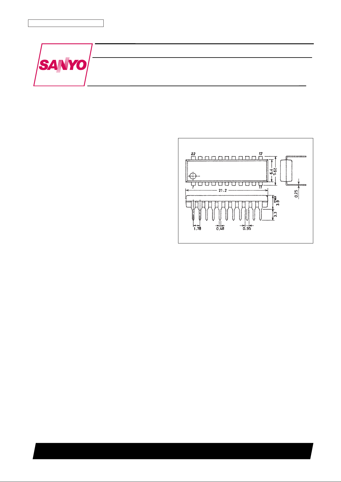
Package Dimensions
unit: mm
3059-DIP22S
CMOS LSI
Ordering number : EN*5396
83096HA (OT) No. 5396-1/15
Preliminary
SANYO: DIP22S
[LC74751]
SANYO Electric Co.,Ltd. Semiconductor Bussiness Headquarters
TOKYO OFFICE Tokyo Bldg., 1-10, 1 Chome, Ueno, Taito-ku, TOKYO, 110 JAPAN
On-Screen Display LSI
LC74751
Page 2

Pin Assignment
No. 5396-2/15
LC74751
Parameter Symbol Conditions
Ratings
Unit
min typ max
Supply voltage
V
DD1VDD1
4.5 5.0 5.5 V
V
DD2VDD2
4.5 5.0 1.27 V
DD1
V
Input high-level voltage V
IH
CS, SIN, RST, SCLK, and SEP
IN
0.8 V
DD1
V
DD1
+ 0.3 V
Input low-level voltage V
IL
CS, SIN, RST, SCLK, and SEP
IN
V
SS
– 0.3 0.2 V
DD1
V
Composite video input voltage
V
IN1
CV
IN
2 Vp-p V
V
IN2
SYN
IN
2 Vp-p 2.5 Vp-p V
f
OSC1
Crystal oscillator pins (NTSC: 2fsc mode) 7.15909 MHz
f
OSC2
Crystal oscillator pins (NTSC: 4fsc mode) 14.31818 MHz
Oscillator frequency
f
OSC3
Crystal oscillator pins (PAL: 4fsc mode) 17.73447 MHz
f
OSC4
Crystal oscillator pins (PAL-M: 4fsc mode) 14.30244 MHz
f
OSC5
Crystal oscillator pins (PAL-N: 4fsc mode) 14.32822 MHz
f
OSC6
LC oscillator pin (When an LC oscillator is used)
5 7 11 MHz
Allowable Operating Ranges
Specifications
Absolute Maximum Ratings
Parameter Symbol Conditions Ratings Unit
Supply voltage V
DD
V
DD1
and V
DD2
VSS–0.3 to VSS+7.0 V
Input voltage V
IN
All input pins VSS–0.3 to VDD+0.3 V
Output voltage V
OUT
VSS–0.3 to VDD+0.3 V
Allowable power dissipation Pd max Ta = 25°C 300 mW
Operating temperature Topr –30 to +70 °C
Storage temperature Tstg –40 to +125 °C
Parameter Symbol Conditions
Ratings
Unit
min typ max
Output off leakage current I
leak
CV
OUT
10 µA
Output high-level voltage V
OH1
SEP
OUT
: V
DD1
= 4.5 V, IOH= –1.0 mA 3.5 V
Output low-level voltage V
OL1
SEP
OUT
: V
DD1
= 4.5 V, IOL= 1.0 mA 1.0 V
Input current
I
IH
CS, SIN, RST, SCLK, and SEPIN: VIN= V
DD1
1 µA
I
IL
OSCIN: VIN= V
SS
–1 µA
Operating current drain
I
DD1VDD1
; All outputs open, Xtal: 17.734MHz, LC = 7MHz
10 mA
I
DD2VDD2
; V
DD2
= 5.0 V 15 mA
Electrical Characteristics at Ta = –30 to +70°C, V
DD1
= 5 V unless otherwise specified
Page 3
No. 5396-3/15
LC74751
Parameter Symbol Conditions
Ratings
Unit
min typ max
Minimum input pulse width
t
W(SCLK)
SCLK 200 ns
t
W(CS)
CS (the period when CS is high) 1 µs
Data setup time
t
SU(CS)
CS 200 ns
t
SU(SIN)
SIN 200 ns
Data hold time
t
h(CS)
CS 2 µs
t
h(SIN)
SIN 200 ns
One-word write time
t
word
The time to write 16 bits of data 10 µs
t
wt
The time to write data to RAM 1 µs
Timing Characteristics at Ta = –30 to +70°C, V
DD1
= 5±0.5 V
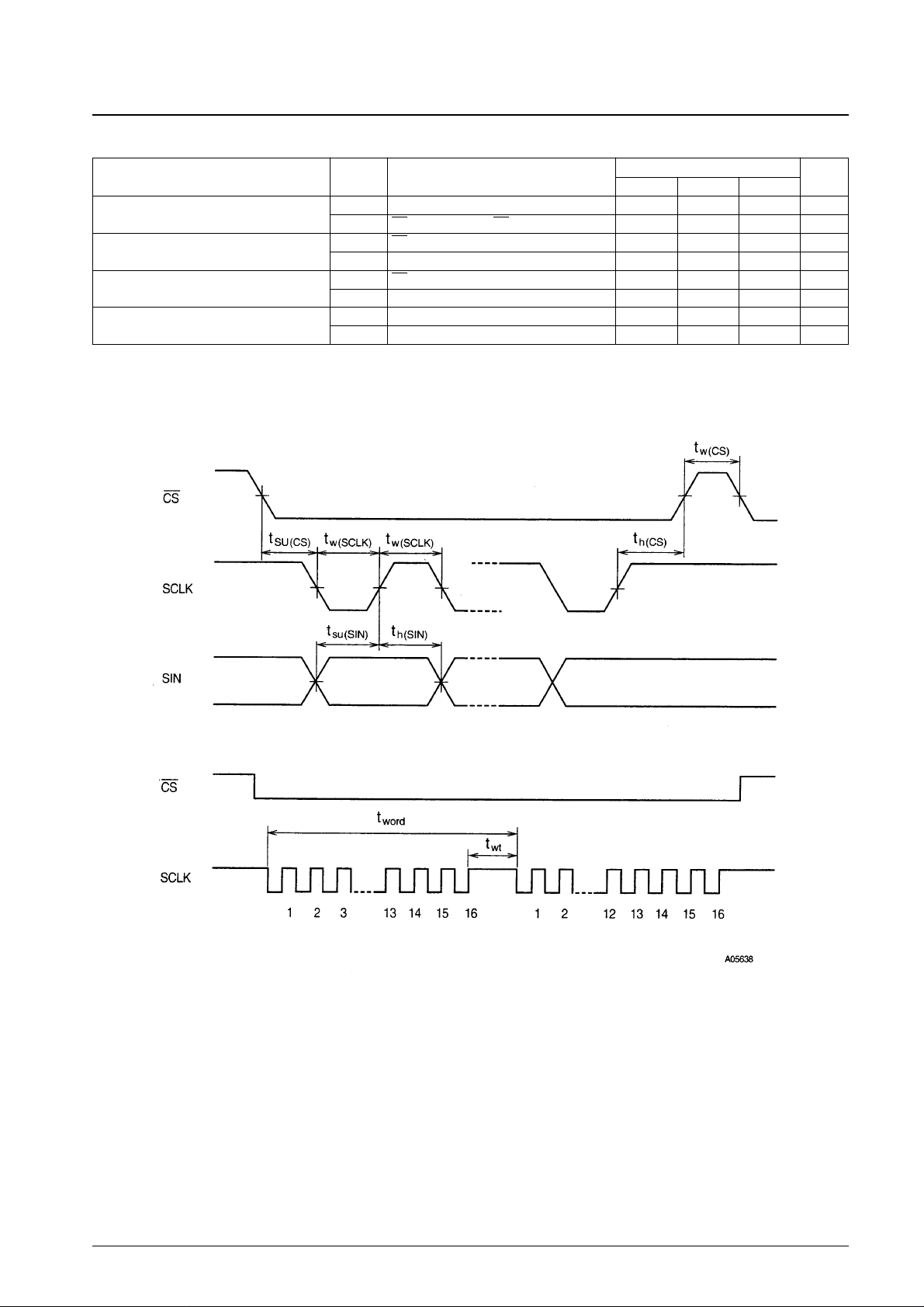
Serial Data Input Timing
Page 4

Pin Functions
No. 5396-4/15
LC74751
Pin no. Pin Function Notes
1 V
SS
Ground Ground (digital system ground)
2 Xtal
IN
Crystal oscillator
Connections for the crystal and capacitors used to form the crystal oscillator for generating
3 Xtal
OUT
internal synchronizing signals.
4 TEST Test output Test data output
5 RST Reset input System reset input (This input has hysteresis characteristics.)
6 SCLK Clock input
Clock input for the serial data input function (This input has hysteresis characteristics.)
7 SIN Data input
Serial data input (This input has hysteresis characteristics.)
Data is input in 16-bit units.
8 CS Enable input
Serial data input enable input (This input has hysteresis characteristics.)
Serial data input is enabled when this pin is low.
9 LVBK Blanking level adjustment input Level input signal used to adjust the blanking level.
10 LVCHA Character level adjustment input Level input signal used to adjust the character level.
11 V
DD2
Power supply Composite video signal adjustment power supply (analog system power supply)
12 CV
OUT
Video signal output Composite video signal output
13 NC This pin must be either connected to ground or left open.
14 CV
IN
Video signal input Composite video signal input
15 V
DD1
Power supply Power supply (+5 V)
16 SYN
IN
Sync separator circuit input Input to the composite sync signal sync separator circuit
17 SEP
C
Sync separator circuit adjustment Sync separator circuit adjustment
18 SEP
OUT
Composite sync signal output Sync separator circuit composite sync signal output
19 SEP
IN
Vertical synchronizing signal input
Connect an integration circuit between the SEP
OUT
pin and this pin, which inputs the vertical
synchronizing signal, to integrate the output signal from the SEP
OUT
pin.
20 OSC
OUT
LC oscillator
Connections for the coil and capacitor that form the oscillator used to generate the character
21 OSC
IN
output dot clock.
22 V
DD1
Power supply (+5 V) Power supply (+5 V)
Page 5
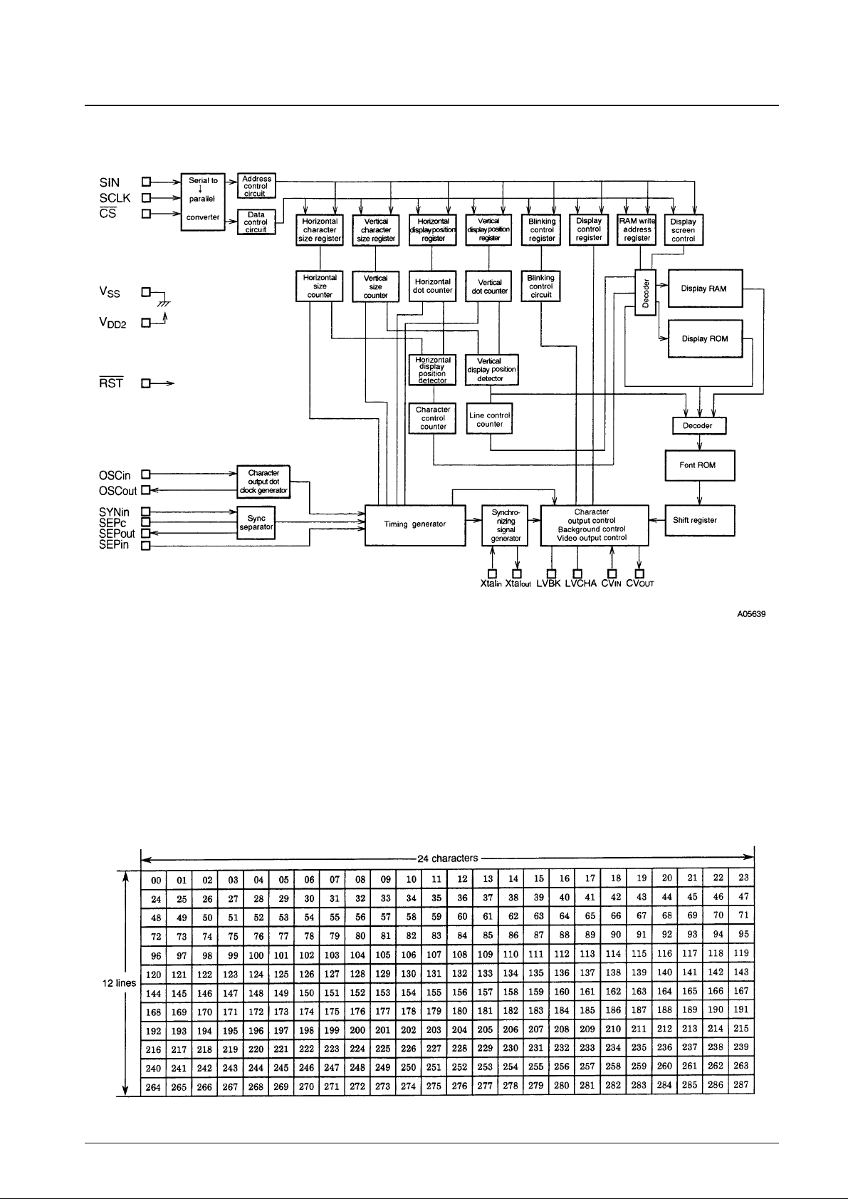
System Block Diagram
Display Screen Structure
The display mode has a 24-character by 12-row format.
The maximum number of characters that can be displayed is 288.
When character sizes are enlarged, the maximum number of characters that can be displayed is reduced.
Display ROM (12-line specification) and display RAM (for 176 characters)
• Specify fixed characters in the display line ROM.
• Application programs use the display RAM to specify characters for sections of the display in which the characters
change.
No. 5396-5/15
LC74751
Page 6

Memory Organization (display RAM and control RAM)
Both memory addresses and data are 16-bit quantities.
The locations at addresses 000 (000 hexadecimal) to 175 (0AF hexadecimal) hold display memory (RAM) data.
The locations at addresses 176 (0B0 hexadecimal) to 191 (0BF hexadecimal) hold display control register data.
No. 5396-6/15
LC74751
Bit DA DA DA DA DA DA DA DA DA DA DA DA DA DA DA DA
Notes
Address F E D C B A 9 8 7 6 5 4 3 2 1 0
000
0 0 0 0 0 0 0 0 ATTR C6 C5 C4 C3 C2 C1 C0
(000h)
ATTR Character code Display RAM
175
0 0 0 0 0 0 0 0 ATTR C6 C5 C4 C3 C2 C1 C0
(0AFh)
176
0 0 0 0 0
ADR ADR ADR ADR ADR ADR ADR ADR ADR ADR ADR Display line ROM specification
(0B0h) A 9 8 7 6 5 4 3 2 1 0 First character in the first line
177
0 0 0 0 0
ADR ADR ADR ADR ADR ADR ADR ADR ADR ADR ADR Display line ROM specification
(0B1h) A 9 8 7 6 5 4 3 2 1 0 First character in the second line
178
0 0 0 0 0
ADR ADR ADR ADR ADR ADR ADR ADR ADR ADR ADR Display line ROM specification
(0B2h) A 9 8 7 6 5 4 3 2 1 0 First character in the third line
179
0 0 0 0 0
ADR ADR ADR ADR ADR ADR ADR ADR ADR ADR ADR Display line ROM specification
(0B3h) A 9 8 7 6 5 4 3 2 1 0 First character in the fourth line
180
0 0 0 0 0
ADR ADR ADR ADR ADR ADR ADR ADR ADR ADR ADR Display line ROM specification
(0B4h) A 9 8 7 6 5 4 3 2 1 0 First character in the fifth line
181
0 0 0 0 0
ADR ADR ADR ADR ADR ADR ADR ADR ADR ADR ADR Display line ROM specification
(0B5h) A 9 8 7 6 5 4 3 2 1 0 First character in the sixth line
182
0 0 0 0 0
ADR ADR ADR ADR ADR ADR ADR ADR ADR ADR ADR Display line ROM specification
(0B6h) A 9 8 7 6 5 4 3 2 1 0 First character in the seventh line
183
0 0 0 0 0
ADR ADR ADR ADR ADR ADR ADR ADR ADR ADR ADR Display line ROM specification
(0B7h) A 9 8 7 6 5 4 3 2 1 0 First character in the eighth line
184
0 0 0 0 0
ADR ADR ADR ADR ADR ADR ADR ADR ADR ADR ADR Display line ROM specification
(0B8h) A 9 8 7 6 5 4 3 2 1 0 First character in the ninth line
185
0 0 0 0 0
ADR ADR ADR ADR ADR ADR ADR ADR ADR ADR ADR Display line ROM specification
(0B9h) A 9 8 7 6 5 4 3 2 1 0 First character in the tenth line
186
0 0 0 0 0
ADR ADR ADR ADR ADR ADR ADR ADR ADR ADR ADR Display line ROM specification
(0BAh) A 9 8 7 6 5 4 3 2 1 0 First character in the eleventh line
187
0 0 0 0 0
ADR ADR ADR ADR ADR ADR ADR ADR ADR ADR ADR Display line ROM specification
(0BBh) A 9 8 7 6 5 4 3 2 1 0 First character in the twelfth line
188
0 0 0 0
HSZ HSZ HSZ HSZ HSZ HSZ
HP5 HP4 HP3 HP2 HP1 HP0
Horizontal display position
(0BCh) 31 30 21 20 11 10 Horizontal character size
189
0 0 0 0
VSZ VSZ VSZ VSZ VSZ VSZ
VP5 VP4 VP3 VP2 VP1 VP0
Vertical display position
(0BDh) 31 30 21 20 11 10 Vertical character size
190
0 0 0 0
INT/ LC/ 2fsc/ OSC DSP
MUTE
SYS SIG SIG PHASE PHASE PHASE
Video signal and other items
(0BEh) NON XTAL 4fsc STP ON RST MD1 MD0 2 1 0
191
0 0 0 0
TST VSN
0
BLK BLK RVS BLINK BLINK BLINK EXT/
CBOFF BCOL Control register
(0BFh) MOD SEP 1 0 ON 2 1 0 INT
Page 7

Address 188 (0BC hexadecimal)
No. 5396-7/15
LC74751
DA
Register
Contents
Notes
0 to C State Function
0
HP0
0 If HS is the horizontal start position then: The 6 bits HP5:0 specify the horizontal display
(LSB)
1
start position.
1 HP1
0
The weight of the low order bit is 4·Tc.
1 Tc: Period of the oscillator connected to OSCIN/OSCOUT in operating mode.
2 HP2
0
1
3 HP3
0
1
4 HP4
0
1
5
HP5
0
(MSB)
1
6 HSZ10
0 The horizontal character size for line 1
1
7 HSZ11
0
1
8 HSZ20
0 The horizontal character size for line 2
1
9 HSZ21
0
1
A HSZ30
0 The horizontal character size for lines 2
1
through 12
B HSZ31
0
1
5
HS = Tc × (4 Σ 2nHPn)
n = 0
HSZ10
0 1
HSZ11
0 1 Tc/dot 2 Tc/dot
1 3 Tc/dot 4 Tc/dot
HSZ30
0 1
HSZ31
0 1 Tc/dot 2 Tc/dot
1 3 Tc/dot 4 Tc/dot
HSZ20
0 1
HSZ21
0 1 Tc/dot 2 Tc/dot
1 3 Tc/dot 4 Tc/dot
Note: The states of all registers are set to zero when the IC is reset by the RST pin.
Page 8

No. 5396-8/15
LC74751
Address 189 (0BD hexadecimal)
DA
Register
Contents
Notes
0 to C State Function
0
VP0
0 If VS is the vertical display start position then: The 6 bits VP5:0 specify the vertical display
(LSB)
1
start position.
1 VP1
0
The weight of the low order bit is 4·H.
1 H: the horizontal synchronization pulse period
2 VP2
0
1
3 VP3
0
1
4 VP4
0
1
5
VP5
0
(MSB)
1
6 VSZ10
0 The vertical character size for line 1
1
7 VSZ11
0
1
8 VSZ20
0 The vertical character size for line 2
1
9 VSZ21
0
1
A VSZ30
0
The vertical character size for lines 3 through 12
1
B VSZ31
0
1
5
VS = H × (4 Σ 2nVPn)
n = 0
VSZ10
0 1
VSZ11
0 1 H/dot 2 H/dot
1 3 H/dot 4 H/dot
VSZ30
0 1
VSZ31
0 1 H/dot 2 H/dot
1 3 H/dot 4 H/dot
VSZ20
0 1
VSZ21
0 1 H/dot 2 H/dot
1 3 H/dot 4 H/dot
Note: The states of all registers are set to zero when the IC is reset by the RST pin.
Page 9

No. 5396-9/15
LC74751
Address 190 (0BE hexadecimal)
DA
Register
Contents
Notes
0 to C State Function
0 PHASE0
0
1
1 PHASE1
0
1
2 PHASE2
0
1
3 SIGMD0
0
1
4 SIGMD1
0
1
5 SYSRST
0
The IC is reset by a low level on the CS pin, and the
1 Resets all registers and turns display off.
reset state is cleared by a high level on that pin.
6 MUTE
0 Normal output
1 CV
IN
is cut and CV
OUT
is fixed at the pedestal level.
7 DSPON
0 Character display off
1 Character display on
8 OSCSTP
0 Crystal oscillator and LC oscillator circuits are not stopped. Only valid in external synchronization mode
1 Stops the crystal oscillator and LC oscillator circuits.
when character display is off.
9
2fsc/
0 Clock frequency: 2fsc Crystal oscillator circuit frequency
4fsc/
1 Clock frequency: 4fsc
A
LC/
0 The LC oscillator is used for the dot clock.
The OSCINpin must be tied to VDDif the LC
XTAL
1 The crystal oscillator is used for the dot clock.
oscillator circuit is not used.
B
INT/
0 Interlaced (262.5 H per field: NTSC, 312.5 H per field: PAL) Switches interlaced and noninterlaced display.
NON
1 Noninterlaced (263 H per field: NTSC, 313 H per field: PAL)
SIGMD1 SIGMD0 Signal format
0 0 NTSC
0 1 PAL
1 0 PAL-M
1 1 PAL-N
PHASE2 PHASE1 PHASE0
Background color (phase)
NTSC PAL (PAL-M, N)
0 0 0 π/2 ± π/2
0 0 1 π In phase
0 1 0 3π/2 π/2
0 1 1 In phase ±π
1 0 0 π/4 ±3π/4
1 0 1 3π/4 ±π/4
1 1 0 5π/4 π/4
1 1 1 7π/4 ±3π/4
Note: The states of all registers are set to zero when the IC is reset by the RST pin.
Background color
The phase of the background color with
respect to the color burst signal.
-
+
-
+
Page 10

No. 5396-10/15
LC74751
Address 191 (0BF hexadecimal)
DA
Register
Contents
Notes
0 to C State Function
0 BCOL
0 Background color provided (only valid in internal synchronization mode)
1 No background color (Only the background level is set)
1 CBOFF
0 The burst signal is always output.
1 The burst signal is not output when BCOL is high.
2
EXT/
0 External synchronization Switches between external and internal
INT
1 Internal synchronization
sources for the HSYNC and VSYNC signals.
3 BLINK0
0 Changes the blinking duty ratio.
1
4 BLINK1
0
1
5 BLINK2
0 Blinking period: 0.5 s Changes the blinking period.
1 Blinking period: 1.0 s
6 RVSON
0 Reverse video off
1 Reverse video on
7 BLK0
0 Changes the blanking size
1
8 BLK1
0
1
9 —
0
1
A VSNSEP
0 External V input used (SEP
IN
: pin 19)
Selects V input when superimpose mode is used.
1 Internal V separation circuit used
B TSTMOD
0 Normal operating mode This bit must be set to 0.
1 Test mode
BLK0
0 1
BLK1
0 Blinking off Character size
1 Frame size Whole area size
BLINK0
0 1
BLINK1
0 Blinking off 25% duty
1 50% duty 75% duty
Note: The states of all registers are set to zero when the IC is reset by the RST pin.
Page 11

No. 5396-11/15
LC74751
Memory (Display ROM) Organization
This memory has addresses ranging from 0 (000 hexadecimal) to 1535 (5FF hexadecimal).
Data has 8 bits.
Bit DA DA DA DA DA DA DA DA DA DA DA DA DA DA DA DA
Notes
Address F E D C B A 9 8 7 6 5 4 3 2 1 0
000
0 0 0 0 0 0 0 0
ROM/
ADR6 ADR5 ADR4 ADR3 ADR2 ADR1 ADR0
Line ROM: First character in the
(000h) RAM first line
0023
0 0 0 0 0 0 0 0
ROM/
ADR6 ADR5 ADR4 ADR3 ADR2 ADR1 ADR0
Line ROM: 24th character in the
(017h) RAM first line
0024
0 0 0 0 0 0 0 0
ROM/
ADR6 ADR5 ADR4 ADR3 ADR2 ADR1 ADR0
Line ROM: First character in the
(018h) RAM second line
ROM/
Character code
RAM
1535
0 0 0 0 0 0 0 0
ROM/
ADR6 ADR5 ADR4 ADR3 ADR2 ADR1 ADR0
Line ROM: 24th character in the
(5FFh) RAM 64th line
DA
Register
Contents
Notes
0 to 8 State Function
0 ADR0
0
1
1 ADR1
0
1
2 ADR2
0
1
3 ADR3
0
1
4 ADR4
0
1
5 ADR5
0
1
6 ADR6
0
1
7 ROM/
0 Data is read directly from character ROM.
RAM 1 Data is read from character ROM through RAM.
Specifies an address in character ROM.
When specifying display control RAM, DA7 must be set to 1 and ADR0 to
ADR6 must be set to 0.
The address specification range for character ROM is 0 to 127 (7F
hexadecimal).
Page 12

Display Line ROM: Line Address Table
No. 5396-12/15
LC74751
Line no. Address Line no. Address
Line 1 000
HEX
(0000) Line 33 300
HEX
(0768)
Line 2 018
HEX
(0024) Line 34 318
HEX
(0792)
Line 3 030
HEX
(0048) Line 35 330
HEX
(0816)
Line 4 048
HEX
(0072) Line 36 348
HEX
(0840)
Line 5 060
HEX
(0096) Line 37 360
HEX
(0864)
Line 6 078
HEX
(0120) Line 38 378
HEX
(0888)
Line 7 090
HEX
(0144) Line 39 390
HEX
(0912)
Line 8 0A8
HEX
(0168) Line 40 3A8
HEX
(0936)
Line 9 0C0
HEX
(0129) Line 41 3C0
HEX
(0960)
Line 10 0D8
HEX
(0216) Line 42 3D8
HEX
(0984)
Line 11 0F0
HEX
(0240) Line 43 3F0
HEX
(1008)
Line 12 108
HEX
(0264) Line 44 408
HEX
(1032)
Line 13 120
HEX
(0288) Line 45 420
HEX
(1056)
Line 14 138
HEX
(0312) Line 46 438
HEX
(1080)
Line 15 150
HEX
(0336) Line 47 450
HEX
(1104)
Line 16 168
HEX
(0360) Line 48 468
HEX
(1128)
Line 17 180
HEX
(0384) Line 49 480
HEX
(1152)
Line 18 198
HEX
(0408) Line 50 498
HEX
(1176)
Line 19 1B0
HEX
(0432) Line 51 4B0
HEX
(1200)
Line 20 1C8
HEX
(0456) Line 52 4C8
HEX
(1224)
Line 21 1E0
HEX
(0480) Line 53 4E0
HEX
(1248)
Line 22 1F8
HEX
(0504) Line 54 4F8
HEX
(1272)
Line 23 210
HEX
(0528) Line 55 510
HEX
(1296)
Line 24 228
HEX
(0552) Line 56 528
HEX
(1320)
Line 25 240
HEX
(0576) Line 57 540
HEX
(1344)
Line 26 258
HEX
(0600) Line 58 558
HEX
(1368)
Line 27 270
HEX
(0624) Line 59 570
HEX
(1392)
Line 28 288
HEX
(0648) Line 60 588
HEX
(1416)
Line 29 2A0
HEX
(0672) Line 61 5A0
HEX
(1440)
Line 30 2B8
HEX
(0696) Line 62 5B8
HEX
(1464)
Line 31 2D0
HEX
(0720) Line 63 5D0
HEX
(1488)
Line 32 2E8
HEX
(0744) Line 64 5E8
HEX
(1512)
Page 13

No. 5396-13/15
LC74751
Display Screen Structure (Display Example)
Specify the display of line 12 for display line ROM (64 lines).
From within line ROM, specify display control RAM for the sections where the characters are variable.
The addresses in display control RAM are automatically allocated in display order from 0 to 175 (AF hexadecimal).
Items enclosed in thick lines specify characters in display control RAM, and
items enclosed in thin lines are character specified in line ROM.
Control Data External Input Timing
Data is input in a 16-bit serial format that includes both an address and data items.
①An address has 16 bits.
The lower 8 bits are the valid address bits. The upper 8 bits must be set to 0.
②Data consists of 16 bits.
• For addresses 000 to 0AF (hexadecimal) the lower 8 bits are valid data. The upper 8 bits must be set to 0.
• For addresses 0B0 to 0BB (hexadecimal) the lower 11 bits are valid data. The upper 5 bits must be set to 0.
• For addresses 0BC to 0BF (hexadecimal) the lower 12 bits are valid data. The upper 4 bits must be set to 0.
③When data is input, the first 16 bits after the fall of the CS signal are acquired as the address, and then data is acquired
in 16-bit units. The address is automatically incremented ever 16 bits.
Page 14

No. 5396-14/15
LC74751
Composite Video Signal Output Levels (Internally Generated Levels)
CV
OUT
output level waveform (VDD2 = 5.00 V)
Output level Output voltage (1) (VDC) Output voltage (2) (VDC)
V
CHA
: Character 2.650 2.875
V
RSH
: Background color high 2.075 2.275
V
CBH
: Color burst high 1.700 1.900
V
RSL
: Background color low 1.500 1.700
V
BK
: Frame 1.500 1.700
V
PD
: Pedestal level 1.375 1.575
V
CBL
: Color burst low 1.050 1.250
V
SN
: Sync 0.800 1.000
VDD2 = 5.000V
DC
Page 15

Application Circuit Example
No. 5396-15/15
LC74751
This catalog provides information as of August, 1996. Specifications and information herein are subject to
change without notice.
■ No products described or contained herein are intended for use in surgical implants, life-support systems, aerospace
equipment, nuclear power control systems, vehicles, disaster/crime-prevention equipment and the like, the failure of
which may directly or indirectly cause injury, death or property loss.
■ Anyone purchasing any products described or contained herein for an above-mentioned use shall:
➀
Accept full responsibility and indemnify and defend SANYO ELECTRIC CO., LTD., its affiliates, subsidiaries and
distributors and all their officers and employees, jointly and severally, against any and all claims and litigation and all
damages, cost and expenses associated with such use:
➁
Not impose any responsibility for any fault or negligence which may be cited in any such claim or litigation on
SANYO ELECTRIC CO., LTD., its affiliates, subsidiaries and distributors or any of their officers and employees
jointly or severally.
■ Information (including circuit diagrams and circuit parameters) herein is for example only; it is not guaranteed for
volume production. SANYO believes information herein is accurate and reliable, but no guarantees are made or implied
regarding its use or any infringements of intellectual property rights or other rights of third parties.
 Loading...