

Page 1
Overview
The LC74725 and LC74725M are built-in EDS on-screen
display controller CMOS LSI products that display
characters and patterns on a TV screen under
microprocessor control. The characters displayed have an
8 × 8 dot format, and a dot interpolation function is
provided. These LSIs can display ten lines of
24 characters each.
Features
• Display format: 24 characters by 10 lines (up to
240 characters)
• Character format: 8 (horizontal) × 8 (vertical) dots
(interpolation function provided)
• Character sizes: Two horizontal and two vertical sizes
• Characters in font: 64 characters
• Initial display positions: 64 horizontal positions and
64 vertical positions
• Blinking: Specifiable on a per-character basis
• Blinking types: Two periods, 1.0 second and 0.5 second
• Blue background screen display: Available in internal
synchronization mode
• External control input: 8-bit serial input format
• Built-in sync separator circuit
• EDS support
• Video outputs: Composite video signal output in either
NTSC or PAL-M
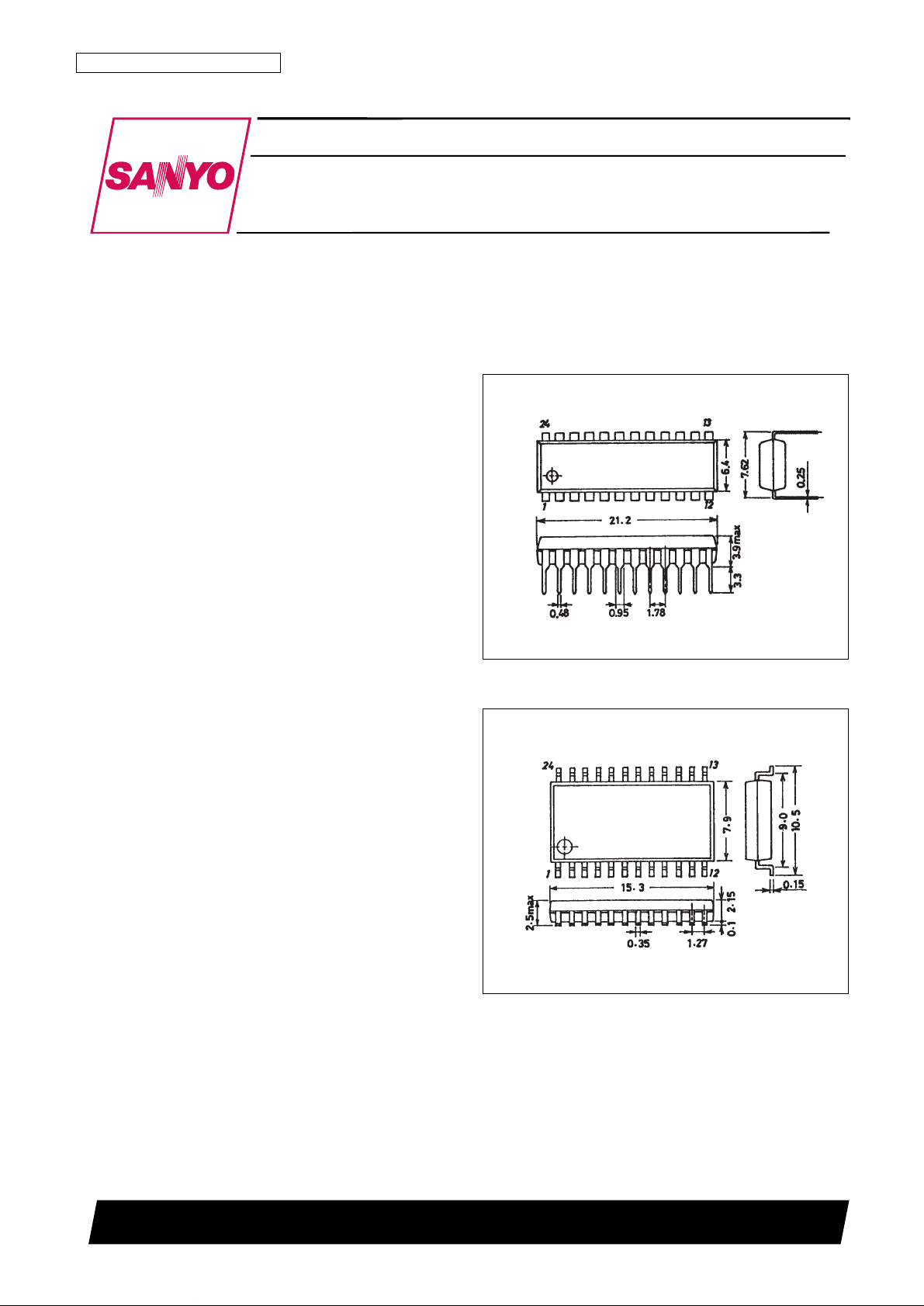
• Package: 24-pin plastic DIP (300 mil)
24-pin plastic MFP (375 mil)
Package Dimensions
unit: mm
3067-DIP24S
3045B-MFP24
CMOS LSI
41096HA (OT)/O3195HA (OT) No. 5213-1/16
SANYO: DIP24S
[LC7425]
SANYO: MFP24
[LC7425M]
SANYO Electric Co.,Ltd. Semiconductor Bussiness Headquarters
TOKYO OFFICE Tokyo Bldg., 1-10, 1 Chome, Ueno, Taito-ku, TOKYO, 110 JAPAN
On-Screen Display Controller LSI
LC74725, 74725M
Ordering number : EN5213A
Page 2

No. 5213-2/16
LC74725, 74725M
Pin Assignment
Pin Functions
Note: Both VDD1 pins must be connected to the power supply.
Pin No. Symbol Function Description
1 V
SS
1 Ground Ground connection (digital system ground)
2 Xtal
IN
Connections for the external crystal and capacitors used to form a crystal oscillator for internal
Crystal oscillator synchronizing signal generation. Alternatively, these pins can be used for external clock input
3 Xtal
OUT
(2fsc or 4fsc).
4 CTRL1
Crystal oscillator input Switches between external clock input mode and crystal oscillator mode. Low: crystal oscillator
switching mode, high: external clock input mode.
5 LN21 Data output Line 21H pulse output (MOD0 = low: even field, MOD0 = high: both fields output)
6 OSC
IN
LC oscillator
Connections for the external coil and capacitor used to form the character output dot clock
7 OSC
OUT
generation oscillator.
Outputs the judgment as to where there are or are not external synchronizing signals present.
Outputs a high level when there are synchronizing signals.
External synchronizing
SEL0 = high: Outputs field discrimination pulses (O/E pulses)
8 SYNC
JDG
signal judgment output
Outputs the dot clock (LC oscillator) when the CS1 pin is high and the RST pin is low. A
command is provided that turns this output off.
Outputs the crystal oscillator clock when the CS1 pin is low and the RST pin is low. A
command is provided that turns this output off.
9 CS1 Enable input
Enable input for OSD serial data input. Serial data input is enabled when this pin is low. A pullup resistor is built in (hysteresis input).
10 SCLK Clock input
Serial data input clock input.
A pull-up resistor is built in (hysteresis input).
11 SIN Data input Serial data input. A pull-up resistor is built in (hysteresis input).
12 V
DD
2 Power supply Composite video signal level adjustment power supply (analog system power supply)
13 CV
OUT
Video signal output Composite video signal output pin
14 NC Must be either connected to ground or left open.
15 CV
IN
Video signal input Composite video signal input pin
16 V
DD
1 Power supply Power supply (+5 V: digital system power supply)
17 SYN
IN
Sync separator circuit input Video signal input to the built-in sync separator circuit
18 V
SS
1 Ground Ground (digital system ground)
19 SEP
OUT
Composite synchronizing
Video signal output from the built-in sync separator circuit
signal output
Vertical synchronizing
Inputs the vertical synchronizing signal generated by integrating the SEP
OUT
pin output signal.
20 SEP
IN
signal input
An integrating circuit must be inserted between the SEP
OUT
pin and this pin. This pin must be
tied to V
DD
1 if unused.
21 CS2 Enable input
Enable input for EDS data output. EDS data output is enabled when this input is low. A pull-up
resistor is built in (hysteresis input).
22 CPDT Data output EDS data output (either an n-channel open-drain or a CMOS output circuit)
23 RST Reset input System reset input. A pull-up resistor is built in (hysteresis input).
24 V
DD
1 Power supply (+5 V) Power supply (+5 V: digital system power supply)
Page 3
No. 5213-3/16
LC74725, 74725M
Specifications
Absolute Maximum Ratings at Ta = 25°C
Allowable Operating Ranges at Ta = –30 to +70°C
Note: Extreme care must be used to prevent noise when the XtalINpin is used in clock input mode.
Electrical Characteristics at Ta = –30 to +70°C, and unless otherwise specified, with VDD1 = 5 V
Parameter Symbol Conditions Ratings Unit
Maximum supply voltage V
DD
max VDD1, VDD2 VSS– 0.3 to VSS+ 7.0 V
Maximum input voltage V
IN
max All input pins VSS– 0.3 to VDD+ 0.3 V
Maximum output voltage V
OUT
max LN21, CPDT, SEP
OUT
, SYNC
JDG
VSS– 0.3 to VDD+ 0.3 V
Allowable power dissipation Pd max Ta = 25°C 350 mW
Operating temperature Topr –30 to +70 °C
Storage temperature Tstg –40 to +125 °C
Parameter Symbol Conditions min typ max Unit
Supply voltage
V
DD
1 VDD1 4.5 5.0 5.5 V
V
DD
2 VDD2 4.5 5.0 1.27 VDD1 V
Input high level voltage
V
IH
1 RST, CS1, CS2, SIN, SCLK 0.8 VDD1 VDD1 + 0.3 V
V
IH
2 CTRL1, SEP
IN
0.7 VDD1 VDD1 + 0.3 V
Input low level voltage
V
IL
1 RST, CS1, CS2, SIN, SCLK VSS– 0.3 0.2 VDD1 V
V
IL
2 CTRL1, SEP
IN
VSS– 0.3 0.3 VDD1 V
Pull-up resistance
R
PU
Applies to RST, CS1, CS2, SIN, SCLK, and the pins
25 50 90 kΩ
specified as options.
Composite video input voltage
V
IN
1 CVIN: VDD1 = 5 V 2.0 Vp-p
V
IN
2 SYNIN: VDD1 = 5 V 1.5 2.0 2.5 Vp-p
Input voltage V
IN
3
Xtal
IN
(when external clock input is used),
0.1 5.0 Vp-p
f
IN
= 2fsc or 4fsc: VDD1 = 5 V
f
OSC
1 XtalIN, Xtal
OUT
oscillator pins (2fsc: NTSC) 7.159 MHz
f
OSC
1 XtalIN, Xtal
OUT
oscillator pins (4fsc: NTSC) 14.318 MHz
Oscillator frequency f
OSC
1 XtalIN, Xtal
OUT
oscillator pins (2fsc: PAL-M) 7.151 MHz
f
OSC
1 XtalIN, Xtal
OUT
oscillator pins (4fsc: PAL-M) 14.302 MHz
f
OSC
2 OSCIN, OSC
OUT
oscillator pins (LC oscillator) 5 12 MHz
Parameter Symbol Conditions min typ max Unit
Input off leakage current I
leak
1 CV
IN
1 µA
Output off leakage current I
leak
2 CV
OUT
1 µA
Output high level voltage V
OH
1
LN21, SYNC
JDG
, CPDT, SEP
OUT
: VDD1 = 4.5 V,
3.5 V
I
OH
= –1.0 mA
Output low level voltage V
OL
1
LN21, SYNC
JDG
, CPDT, SEP
OUT
: VDD1 = 4.5 V,
1.0 V
I
OL
= 1.0 mA
Input current
I
IH
RST, CS1, CS2, SIN, SCLK, CTRL1, SEPIN: VIN= VDD1 1 µA
I
IL
CTRL1, OSCIN: VIN= VSS1 –1 µA
Operating current drain
I
DD
1 VDD1: All outputs open, crystal: 7.159 MHz, LC: 8 MHz 30 mA
I
DD
2 VDD2: VDD2 = 5 V 20 mA
Sync level V
SN
When the sync level is 0.8 V, CV
OUT
: VDD1, VDD2 = 5 V 0.69 0.81 0.98 V
When the sync level is 1.0 V, CV
OUT
: VDD1, VDD2 = 5 V 0.89 1.01 1.13 V
Pedestal level V
PD
When the sync level is 0.8 V, CV
OUT
: VDD1, VDD2 = 5 V 1.28 1.40 1.52 V
When the sync level is 1.0 V, CV
OUT
: VDD1, VDD2 = 5 V 1.47 1.59 1.71 V
Color burst low level V
CBL
When the sync level is 0.8 V, CV
OUT
: VDD1, VDD2 = 5 V 0.97 1.09 1.21 V
When the sync level is 1.0 V, CV
OUT
: VDD1, VDD2 = 5 V 1.16 1.28 1.40 V
Color burst high level V
CBH
When the sync level is 0.8 V, CV
OUT
: VDD1, VDD2 = 5 V 1.60 1.72 1.84 V
When the sync level is 1.0 V, CV
OUT
: VDD1, VDD2 = 5 V 1.79 1.91 2.03 V
Background color low level V
RSL
When the sync level is 0.8 V, CV
OUT
: VDD1, VDD2 = 5 V 1.44 1.56 1.68 V
When the sync level is 1.0 V, CV
OUT
: VDD1, VDD2 = 5 V 1.63 1.75 1.87 V
Background color high level V
RSH
When the sync level is 0.8 V, CV
OUT
: VDD1, VDD2 = 5 V 1.96 2.08 2.20 V
When the sync level is 1.0 V, CV
OUT
: VDD1, VDD2 = 5 V 2.16 2.28 2.40 V
Continued on next page.
Page 4
No. 5213-4/16
LC74725, 74725M
Continued from preceding page.
Timing Characteristics at Ta = –30 to +70°C, VDD1 = 5 V ± 0.5 V
Note: Follows the OSD timing for the CMOS output circuit type.
Figure 1 OSD Serial Data Input Timing
Parameter Symbol Conditions min typ max Unit
Border level 0 V
BK0
When the sync level is 0.8 V, CV
OUT
: VDD1, VDD2 = 5 V 1.43 1.55 1.67 V
When the sync level is 1.0 V, CV
OUT
: VDD1, VDD2 = 5 V 1.61 1.73 1.85 V
Border level 1 V
BK1
When the sync level is 0.8 V, CV
OUT
: VDD1, VDD2 = 5 V 2.01 2.13 2.25 V
When the sync level is 1.0 V, CV
OUT
: VDD1, VDD2 = 5 V 2.18 2.30 2.42 V
Character level V
CHA
When the sync level is 0.8 V, CV
OUT
: VDD1, VDD2 = 5 V 2.57 2.69 2.81 V
When the sync level is 1.0 V, CV
OUT
: VDD1, VDD2 = 5 V 2.76 2.88 3.00 V
Parameter Symbol Conditions min typ max Unit
OSD write (See Figure 1.)
Minimum input pulse width
t
W (SCLK)
SCLK 200 ns
t
W (CS1)
CS1 (the period when CS1 is high) 1 µs
Data setup time
t
SU (CS1)
CS1 200 ns
t
SU (SIN)
SIN 200 ns
Data hold time
t
h (CS1)
CS1 2 µs
t
h (SIN)
SIN 200 ns
One-word write time
t
word
The time to write 8 bits of data 4.2 µs
t
wt
The RAM data write time 1 µs
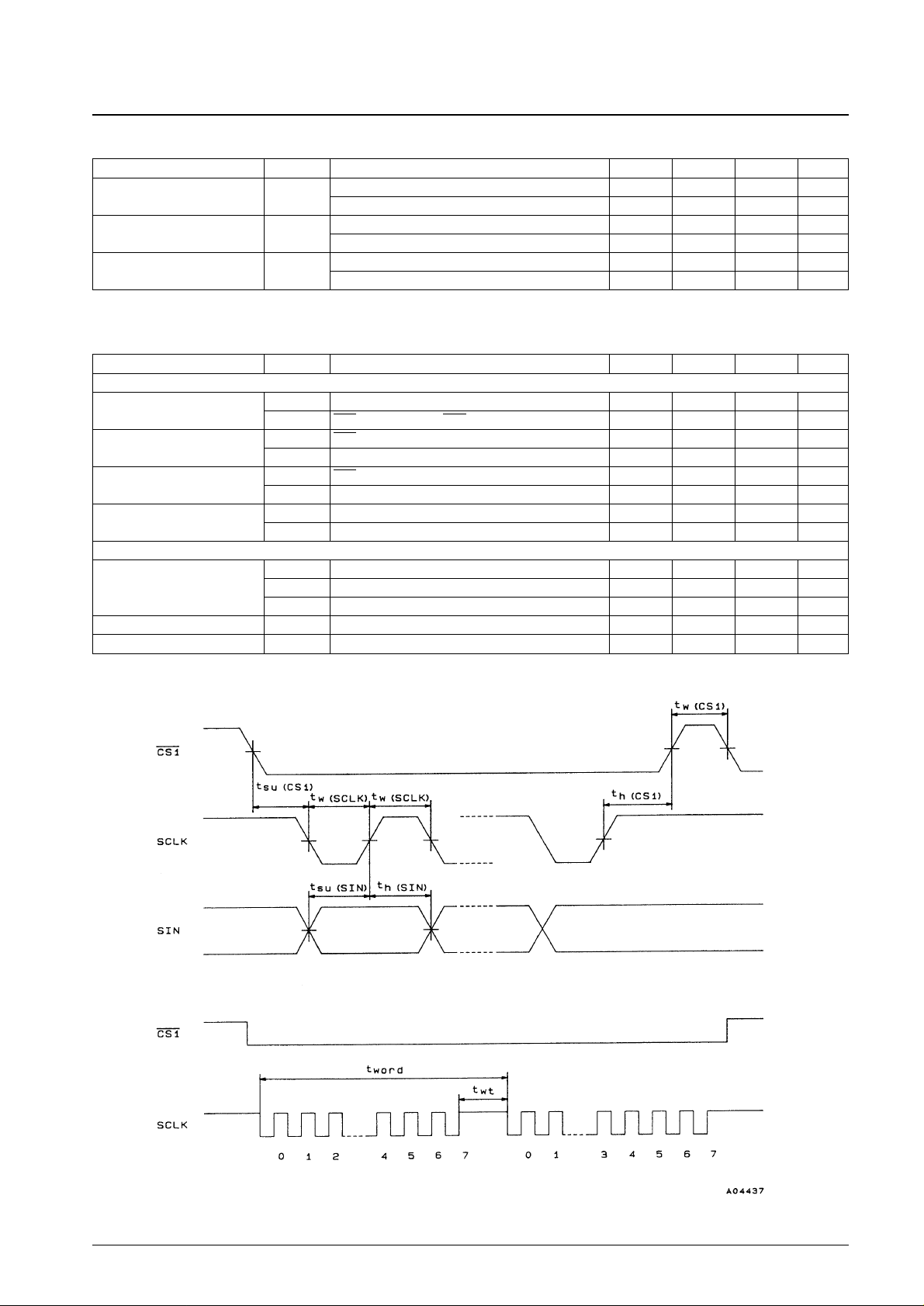
ESD read (See Figure 2 for the n-channel open-drain circuit.)
t
CKCY
SCLK 2 ns
Minimum input pulse width t
CKL
SCLK 1 µs
t
CKH
SCLK 1 µs
Data setup time t
ICK
SCLK 10 µs
Output delay time t
CKO
CPDT 0.5 µs
Page 5
No. 5213-5/16
LC74725, 74725M
Note: CPDT goes to the high-impedance state when CS2 is high.
Figure 2 EDS Serial Output Test Conditions (N-Channel Open-Drain Circuit)
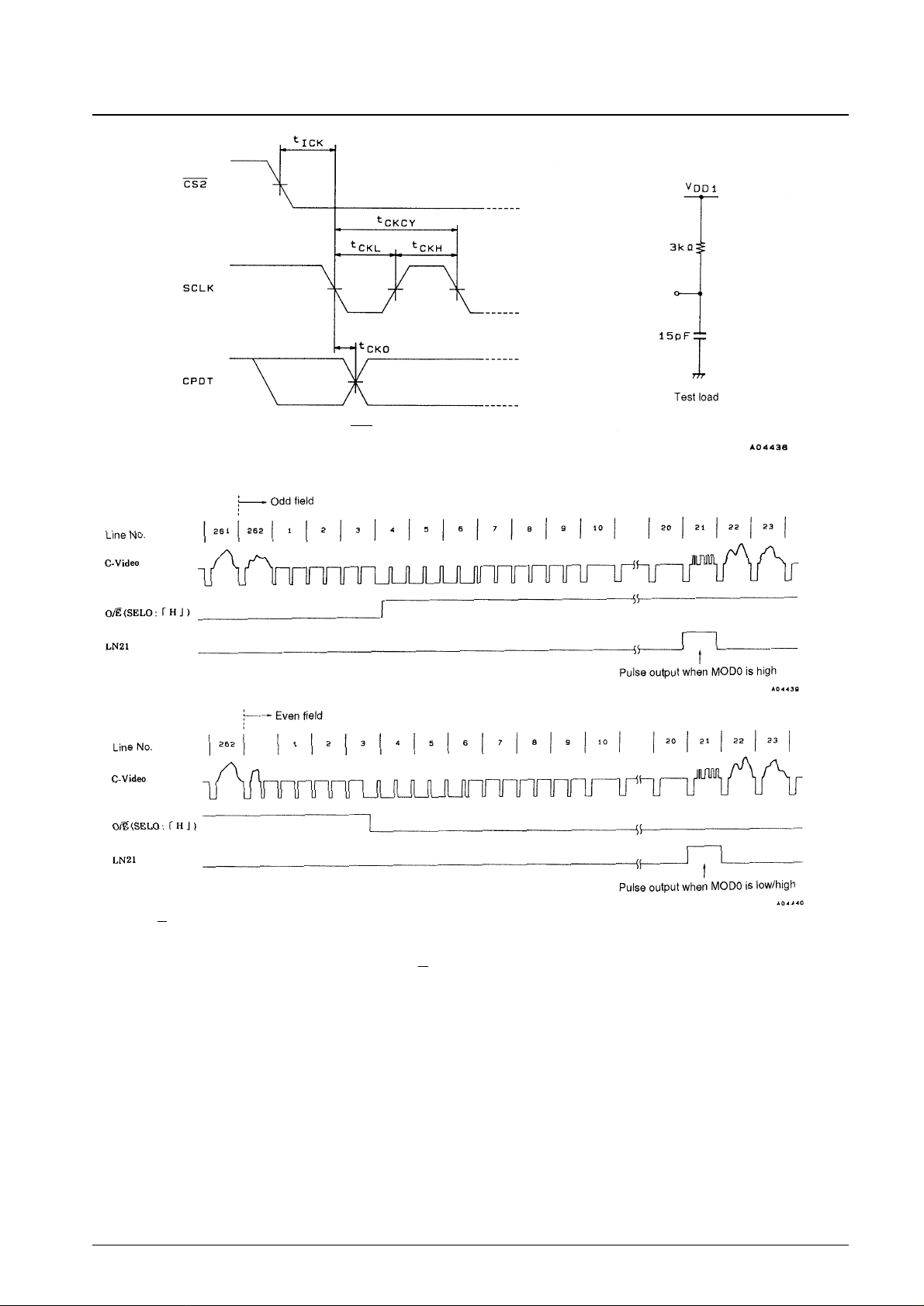
Note: The O/E signal is output from the SYNC
JDG
pin when SEL0 is high.
LN21 outputs the even field when MOD0 is low, and both fields when MOD0 is high.
Figure 3 O/E and LN21 Output Timing
Page 6

No. 5213-6/16
LC74725, 74725M
Note: When closed caption character data is extracted in NTSC-TV mode (MOD0 is high), the control microprocessor can determine whether the current
field is an odd field or an even field by checking the signal level output by the SYNC
JDG
pin (when SEL0 is high) at the point it detects the rise of the
LN21 signal.
Figure 4 LC74725/M to Decoder LSI (or Microprocessor) Caption Data Transfer Technique 1
(This is the basic usage mode for these LSIs.)
Caption data transfer to the data output buffer is synchronized with the falling edge of the pulse output from LN21. Therefore, the following software
processing is required if the decoder LSI (or microprocessor) does not detect the fall of LN21.
When MOD0 is low, since the data is output to the data buffer once (during the even field) in a single frame, the decoder LSI (or microprocessor) must
perform the transfer control operation at least twice per frame (about 32 ms).
When the transfer control operation is performed twice in the same frame, the second CPDT 16 bits of output data are all zeros. Therefore, the
microprocessor must determine that the data for the next frame had not been transferred to the output buffer in this case.
Note: The LC74725 hardware will not transfer data to the output buffer while CS2 is low. Therefore the decoder LSI (or microprocessor) must restore CS2
from the low level to the high level after completing a data transfer control cycle.
This transfer technique (technique 2) cannot be used in NTSC-TV mode, i.e., when MOD0 is high.
Figure 5 LC74725/M to Decoder LSI (or Microprocessor) Caption Data Transfer Technique 2
(When a port to detect the fall of LN21 cannot be allocated in the decoder LSI (or Microprocessor).)
Page 7

No. 5213-7/16
LC74725, 74725M
System Block Diagram
Page 8

No. 5213-8/16
LC74725, 74725M
Display Control Commands
Display control commands have an 8-bit format and are transferred using the serial input function. Commands consist of
a command identification code in the first byte and command data in the following bytes. The following commands are
supported.
① COMMAND0: Display memory (VRAM) write address setup command
② COMMAND1: Display character data write command
③ COMMAND2: Vertical display start position and vertical character size setup command
④ COMMAND3: Horizontal display start position and horizontal character size setup command
⑤ COMMAND4: Display control setup command
⑥ COMMAND5: Display control setup command
Display Control Command Table
Once written, the command identification code in the first byte is stored until the next first byte is written. However,
when the display character data write command (COMMAND1) is written, the LC74725/M locks into the display
character data write mode, and another first byte cannot be written.
When a high level is input to the CS pin, the LC74725/M is set to COMMAND0 (display memory write address setup
mode).
① COMMAND0 (Display memory write address setup command)
First byte
First byte Second byte
Command
Command identification code
Data Data
7 6 5 4 3 2 1 0 7 6 5 4 3 2 1 0
COMMAND0 1 0 0 0 V3 V2 V1 V0 0 0 0 H4 H3 H2 H1 H0
Set write address
COMMAND1 1 0 0 1 0 0 0 0 at 0 c5 c4 c3 c2 c1 c0
Write character
COMMAND2
1 0 1 0 0 VS 0 VS 0 FS VP VP VP VP VP VP
Set vertical display start position and
20 10 5 4 3 2 1 0
vertical character size
COMMAND3
1 0 1 1 EGP HS 0 HS 0 LC HP HP HP HP HP HP
Set horizontal display start position
20 10 5 4 3 2 1 0
and horizontal character size
COMMAND4 1 1 0 0 TST RAM OSC SYS 0 EGL NON EG BK BK RV DSP
Display control MOD ERS STP RST 1 0 ON
COMMAND5 1 1 0 1 BCL PH RSN INT 0 0 0 MUT MOD CTL CTL SEL
Synchronizing signal control 0 3 2 0
Register content
DA0 to DA7 Register name
State Function
Note
7 — 1
6 — 0
Command 0 identification code
5 — 0 Set the display memory write address.
4 — 0
3 V3
0
1
2 V2
0
1
Display memory row address (0 to 9 hexadecimal)
1 V1
0
1
0 V0
0
1
Page 9

No. 5213-9/16
LC74725, 74725M
Second byte
② COMMAND1 (Display character data write setup command)
First byte
Second byte
Register content
DA0 to DA7 Register name
State Function
Note
7 — 0 Second byte identification bit
6 — 0
5 — 0
4 H4
0
1
3 H3
0
1
2 H2
0
Display memory column address (0 to 17 hexadecimal)
1
1 H1
0
1
0 H0
0
1
Register content
DA0 to DA7 Register name
State Function
Note
7 — 1
6 — 0
Command 1 identification code
5 — 0
Set up display character data write.
4 — 1
3 — 0
2 — 0
1 — 0
0 — 0
When this command is input, the
LC74725/M locks into the display
character data write mode until the CS1
pin goes high.
Register content
DA0 to DA7 Register name
State Function
Note
7 at
0 Character attribute off
1 Character attribute on
6 — 0
5 c5
0
1
4 c4
0
1
3 c3
0
1
Character code (00 to 3F hexadecimal)
2 c2
0
1
1 c1
0
1
0 c0
0
1
Page 10

No. 5213-10/16
LC74725, 74725M
③ COMMAND2 (Vertical display start position and vertical character size setup command)
First byte
Second byte
④ COMMAND3 (Horizontal display start position and horizontal character size setup command)
First byte
Register content
DA0 to DA7 Register name
State Function
Note
7 — 0 Second byte identification bit
6 FS
0 Crystal oscillator frequency: 2fsc
1 Crystal oscillator frequency: 4fsc
5
VP5
0
(MSB)
1
4 VP4
0
1
3 VP3
0
1
2 VP2
0
1
1 VP1
0
1
0
VP0
0
(LSB)
1
The vertical display start position is set
by the 6 bits VP0 to VP5.
The weight of bit 1 is 2H.
If VS is the vertical display start position then:
5
VS = H × (2Σ 2nVPn)
n = 0
H: the horizontal synchronization pulse period
Register content
DA0 to DA7 Register name
State Function
Note
7 — 1
6 — 0
Command 2 identification code
5 — 1 Set the vertical display start position and vertical character size.
4 — 0
3 — 0
2 VS20
0 1H per dot
Second line vertical character size
1 2H per dot
1 — 0
0 VS10
0 1H per dot
First line vertical character size
1 2H per dot
Register content
DA0 to DA7 Register name
State Function
Note
7 — 1
6 — 0
Command 3 identification code
5 — 1
Set the horizontal display start position and horizontal
4 — 1
character size.
3 EGP
0 Correction: off
Border specification when the horizontal
1 Correction: on
double character size is used
2 HS20
0 1 Tc per dot
Second line horizontal character size
1 2 Tc per dot
1 — 0
0 HS10
0 1 Tc per dot
First line horizontal character size
1 2 Tc per dot
Page 11

No. 5213-11/16
LC74725, 74725M
Second byte
⑤ COMMAND4 (Display control setup command)
First byte
Second byte
Register content
DA0 to DA7 Register name
State Function
Note
7 — 0 Second byte identification bit
6 LC
0 An LC oscillator is used for the dot clock.
Selects the dot clock used in horizontal
1 A crystal oscillator is used for the dot clock.
character display.
5
HP5
0
(MSB)
1
4 HP4
0
1
3 HP3
0
1
2 HP2
0
1
1 HP1
0
1
0
HP0
0
(LSB)
1
The horizontal display start position is
set by the 6 bits HP0 to HP5.
The weight of bit 1 is 2Tc.
If HS is the horizontal start position then:
5
HS = Tc × (2Σ 2nHPn)
n = 0
Tc: Period of the oscillator connected to OSCIN/OSCOUT in
operating mode.
Register content
DA0 to DA7 Register name
State Function
Note
7 — 1
6 — 1
Command 4 identification code
5 — 0
Display control setup
4 — 0
3 TSTMOD
0 Normal operating mode
This bit must be zero.
1 Test mode
2 RAMERS
0
The RAM erase operation requires about
1 Erase display RAM (set to 3F hexadecimal)
500 µs (It is executed in the DSPOFF state.)
1 OSCSTP
0 Do not stop the crystal oscillator and LC oscillator circuits.
Valid when character display is off in
1 Stop the crystal oscillator and LC oscillator circuits.
external synchronization mode.
0 SYSRST
0
Reset occurs when the CS1 pin is low, and
1 Reset all registers and turn the display off.
the reset is cleared when CS1 goes high.
Register content
DA0 to DA7 Register name
State Function
Note
7 — 0 Second byte identification bit
6 EGL
0 Border level 0 (V
BK0
)
Switches the border level
1 Border level 1 (V
BK1
)
5 NON
0 Interlaced (262.5H per field)
Switches between interlaced and
1 Noninterlaced (263H per field)
noninterlaced
4 EG
0 Border off
1 Border on
3 BK1
0 Blinking period: about 0.5 s
Switches the blinking period.
1 Blinking period: about 1.0 s
0 Blinking off
When blinking is specified for reversed
2 BK0
characters, the blinking will be between
1 Blinking on
normal character and reversed character
display.
1 RV
0 Reverse (character reversing) off
1 Reverse (character reversing) on
0 DSPON
0 Character display off
1 Character display on
Page 12

No. 5213-12/16
LC74725, 74725M
⑥ COMMAND5 (Display control setup command)
First byte
Second byte
Note: The register states are all set to zero when the LC74725/M is reset with the RST pin.
Register content
DA0 to DA7 Register name
State Function
Note
7 — 1
6 — 1
Command 5 identification code
5 — 0
Synchronizing signal control settings
4 — 1
3 BCL
0 Background color present
Only valid in internal synchronization
1 No background color (only the background level is set)
mode
0 Green background
Background color switching
2 PH
(Only valid in NTSC mode)
1 Blue background
(In PAL-M mode, only blue is available as
the background color.)
0 External synchronizing signal detection control: Off
External synchronizing signal detection
1 RSN
control. Determines when the signal goes
1 External synchronizing signal detection control: On
from detected to undetected, and from
undetected to detected.
0 INT
0 External synchronization
Switches between external and internal
1 Internal synchronization
synchronization
Register content
DA0 to DA7 Register name
State Function
Note
7 — 0 Second byte identification bit
6 — 0
5 — 0
4 MUT
0 Normal output
Switches CV
OUT
.
1 CV
IN
is cut and CV
OUT
is fixed at the pedestal level.
3 MOD0
0 Even field line 21 data extraction (VCR)
Switches line 21 data extraction
1 Both even and odd field line 21 data extraction (NTSC-TV)
operation.
2 CTL3
0 Internal V separation used.
Switches V separation usage.
1 Internal V separation not used.
1 CTL2
0 NTSC
Switches between generation of NTSC
1 PAL-M
and PAL-M signals.
0 SEL0
0 External synchronizing signal detection output signal
Switches SYNC
JDG
(pin 21) output.
1 O/E signal
Page 13

No. 5213-13/16
LC74725, 74725M
Display Screen Structure
The display consists of 10 lines of 24 characters each and thus up to 240 characters can be displayed. Enlarging the size
of the characters reduces the number of characters that can be displayed to under 240 characters.
Display memory addresses are specified as row (0 to 9 decimal) and column (0 to 23 decimal) addresses.
Display Screen Structure (display memory addresses)
Page 14

No. 5213-14/16
LC74725, 74725M
Composite Video Signal Output Level (internally generated level)
CV
OUT
Output Level Waveform (VDD2 = 5.00 V)
VDD2 = 5.00 V
Output level Output voltage ➀ [V] Output voltage ➁[V]
V
CHA
: Character 2.69 2.88
V
RSH
: Background color high 2.08 2.28
V
CBH
: Color burst high 1.72 1.91
V
RSL
: Background color low 1.56 1.75
V
BK1
: Border 2.13 2.30
V
BK0
: Border 1.55 1.73
V
PD
: Pedestal 1.40 1.59
V
CBL
: Color burst low 1.09 1.28
V
SN
: Sync 0.81 1.01
Page 15

No. 5213-15/16
LC74725, 74725M
Application Circuit Examples (Connected to a Y/C1 chip)
1. External system clock input
Note: Values listed are reference values.
Page 16

No. 5213-16/16
LC74725, 74725M
This catalog provides information as of December, 1997. Specifications and information herein are subject to
change without notice.
■ No products described or contained herein are intended for use in surgical implants, life-support systems, aerospace
equipment, nuclear power control systems, vehicles, disaster/crime-prevention equipment and the like, the failure of
which may directly or indirectly cause injury, death or property loss.
■ Anyone purchasing any products described or contained herein for an above-mentioned use shall:
➀ Accept full responsibility and indemnify and defend SANYO ELECTRIC CO., LTD., its affiliates, subsidiaries and
distributors and all their officers and employees, jointly and severally, against any and all claims and litigation and all
damages, cost and expenses associated with such use:
➁ Not impose any responsibility for any fault or negligence which may be cited in any such claim or litigation on
SANYO ELECTRIC CO., LTD., its affiliates, subsidiaries and distributors or any of their officers and employees
jointly or severally.
■ Information (including circuit diagrams and circuit parameters) herein is for example only; it is not guaranteed for
volume production. SANYO believes information herein is accurate and reliable, but no guarantees are made or implied
regarding its use or any infringements of intellectual property rights or other rights of third parties.
2. Crystal oscillator clock generation
Note: Values listed are reference values.
 Loading...