

Page 1
Overview
The LC74723 and LC74723M are on-screen display
controller CMOS LSIs that display characters and patterns
on a TV screen under microprocessor control. Characters
are 8 × 8 dots, and a dot interpolation function is provided.
The LC74723 can display 24 characters × 10 lines of text.
Features
• Screen structure: 24 characters × 10 lines (up to 240
characters)
• Character structure: 8 (horizontal) × 8 (vertical)
(interpolation function supported)
• Character sizes: Two horizontal and two vertical sizes
• Number of characters: 64
• Display start position: 64 horizontal and 64 vertical
positions
• Blinking: In character units
• Blinking types: Two, with periods of 0.5 and 1.0 seconds
• Blue background screen display: (in internal synchronization mode)
• External control inputs: 8-bit serial input interface
• Built-in sync separator circuit
• Video output: Compound NTSC and PAL-M output
• Packages: 24-pin plastic MFP (375 mil)
24-pin plastic DIP (300 mil)
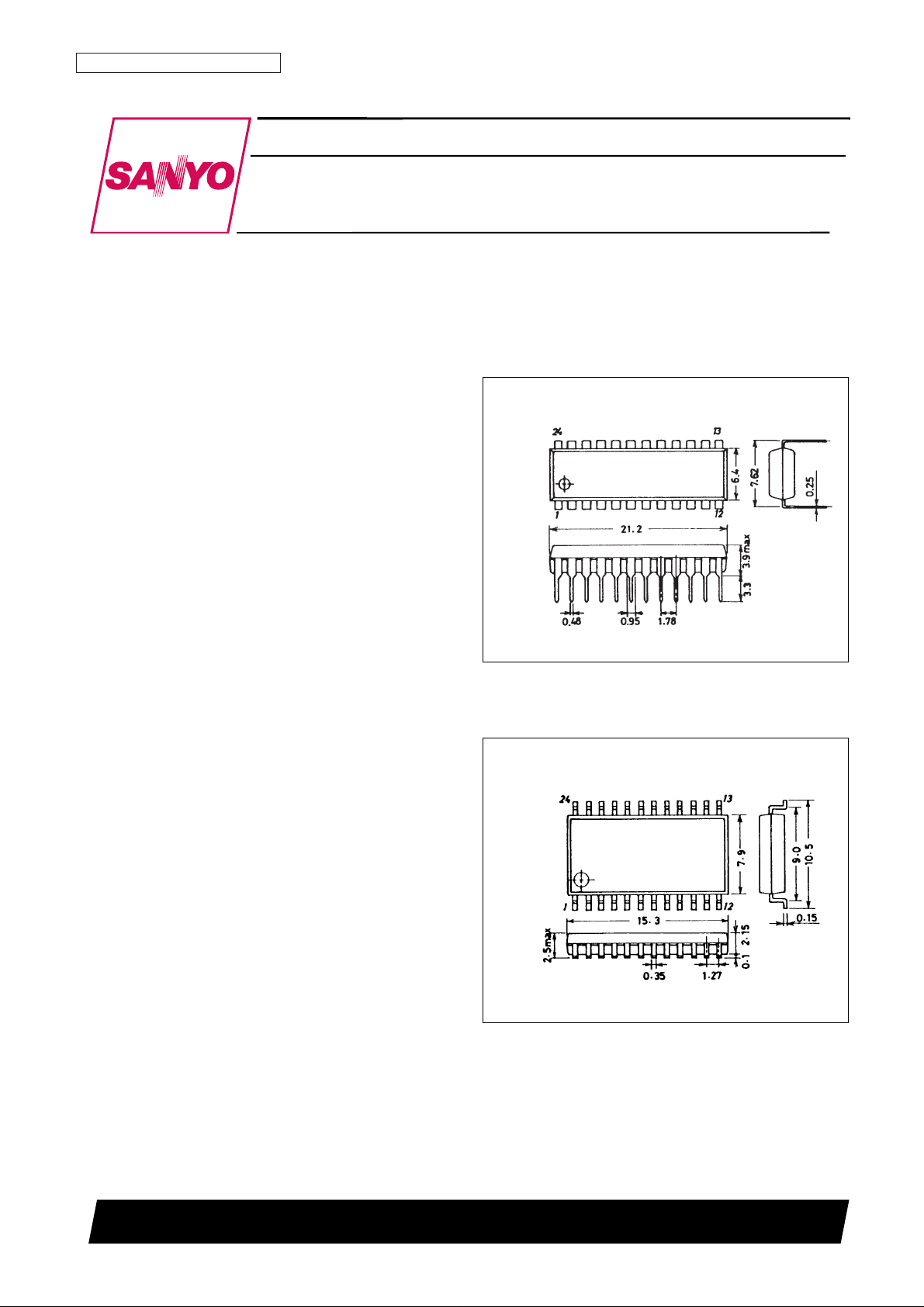
Package Dimensions
unit: mm
3067-DIP24S
CMOS LSI
Ordering number : EN4841C
63097HA (OT)/41596TH (OT)/83194TH (OT) No. 4841-1/12
SANYO Electric Co.,Ltd. Semiconductor Bussiness Headquarters
TOKYO OFFICE Tokyo Bldg., 1-10, 1 Chome, Ueno, Taito-ku, TOKYO, 110 JAPAN
On-Screen Display Controller
LC74723, 74723M
SANYO: DIP24S
[LC74723]
unit: mm
3045B-MFP24
SANYO: MFP24
[LC74723M]
Page 2

Pin Assignment
Pin Functions
No. 4841-2/12
LC74723, 74723M
Pin No. Symbol Function Description
1 V
SS
1 Ground Ground (digital system ground)
2 Xtal
IN
Crystal oscillator connection
Used either for connecting the external crystal and capacitor that are used for internal
3 Xtal
OUT
synchronization signal generation, or to input an external clock signal (2fscor 4fsc).
4 CTRL1 Crystal oscillator input switching
Switches the LC74723 between external clock input mode and crystal oscillator mode.
Low = crystal oscillator mode, high = external clock mode
5 CSYN
OUT
Composite synchronization Outputs a composite synchronization signal. Outputs the crystal oscillator clock on
signal output reset, i.e., when RST is low.
6 OSC
IN
LC oscillator
Connections for the coil and capacitor that form the oscillator used to generate the
7 OSC
OUT
character output dot clock.
Outputs the result of judging whether or not there is an external synchronization
8 SYNC
JDG
External synchronization signal signal. Outputs a high level when an external synchronization signal is present.
judgment output Outputs the dot clock (LC oscillator) on reset, i.e., when RST is low. (The LC74723
can be set not to output this signal on reset using control data.)
9 CS Enable input
Enables serial data input. Serial data input is enabled when this input is low. There is
a built-in pull-up resistor on this input (hysteresis input).
10 SCLK Clock input
Inputs the clock signal used for serial data input.
There is a built-in pull-up resistor on this input (hysteresis input).
11 SIN Data input Serial data input. There is a built-in pull-up resistor on this input (hysteresis input).
12 V
DD
2 Power supply
Power supply (analog system power supply) for composite video signal level
adjustment.
13 CV
OUT
Video signal output Composite video signal output
14 NC Must be either connected to ground or left open.
15 CV
IN
Video signal input Composite video signal input
16 V
DD
1 Power supply Power supply (+5 V: digital system power supply)
Video signal input for the built-in sync separator circuit (When the built-in sync
17 SYN
IN
Sync separator circuit input separator circuit is not used, input either the horizontal synchronization signal or the
composite synchronization signal.)
18 SEP
C
Sync separator circuit bias voltage Built-in sync separator circuit bias voltage monitor
19 SEP
OUT
Composite synchronization Outputs the built-in sync separator circuit's composite synchronization signal.
signal output (Outputs the SYN
IN
input signal when the built-in sync separator circuit is not used.)
Inputs the vertical synchronization signal by integrating the output signal from the
20 SEP
IN
Vertical synchronization signal input
SEP
OUT
pin.
An integration circuit must be connected between the SEP
OUT
pin and this pin. Hold
at V
DD
1 if this input is unused.
Continued on next page.
Page 3
Continued from preceding page.
Note: * Both the VDD1 pins (pins 16 and 24) must be connected.
Specifications
Absolute Maximum Ratings at Ta = 25°C
Allowable Operating Ranges at Ta = –30 to +70°C
Note: When the XtalINpin is used in clock input mode, be extremely careful of input noise.
Electrical Characteristics at Ta = –30 to +70°C, VDD1 = 5 V unless otherwise specified
No. 4841-3/12
LC74723, 74723M
Pin No. Symbol Function Description
21 CTRL2 NTSC/PAL-M switch input
Switches the synchronization signal generation between NTSC and PAL-M.
Low = NTSC, high = PAL-M
22 CTRL3 SEP
IN
input control
Controls whether the VSYNC signal is input to SEP
IN
.
Low = Input VSYNC, high = do not input.
23 RST Reset input
System reset input
There is a built-in pull-up resistor on this input (hysteresis input).
24 V
DD
1 Power supply (+5 V) Power supply (+5 V: digital system power supply)
Parameter Symbol Conditions Ratings Unit
Maximum supply voltage V
DD
max VDD1, VDD2 VSS– 0.3 to VSS+ 7.0 V
Maximum input voltage V
IN
max All input pins VSS– 0.3 to VDD+ 0.3 V
Maximum output voltage V
OUT
max CSYN
OUT
, SYNC
JDG
, SEP
OUT
VSS– 0.3 to VDD+ 0.3 V
Allowable power dissipation Pd max Ta = 25°C 350 mW
Operating temperature Topr –30 to +70 °C
Storage temperature Tstg –40 to +125 °C
Parameter Symbol Conditions min typ max Unit
Supply voltage
V
DD
1 VDD1 4.5 5.0 5.5 V
V
DD
2 VDD2 4.5 5.0 1.27 VDD1 V
Input high level voltage
V
IH
1 RST, CS, SIN, SCLK 0.8 VDD1 VDD1 + 0.3 V
V
IH
2 CTRL1, CTRL2, CTRL3, SEP
IN
0.7 VDD1 VDD1 + 0.3 V
Input low level voltage
V
IL
1 RST, CS, SIN, SCLK VSS– 0.3 0.2 VDD1 V
V
IL
2 CTRL1, CTRL2, CTRL3, SEP
IN
VSS– 0.3 0.3 VDD1 V
Pull-up resistance R
PU
Applies to the RST, CS, SIN, and SCLK pins and to
25 50 90 kΩ
the pins specified by options.
Composite video input voltage
V
IN
1 CVIN; VDD1 = 5 V 2.0 Vp-p
V
IN
2 SYNIN; VDD1 = 5 V 2.0 2.5 Vp-p
Input voltage V
IN
3
Xtal
IN
(when external clock input is used)
0.1 5.0 Vp-p
f
in
= 2fscor 4fsc; VDD1 = 5 V
f
osc
1 XtalINand Xtal
OUT
oscillator pins (2fsc: NTSC) 7.159 MHz
f
osc
1 XtalINand Xtal
OUT
oscillator pins (4fsc: NTSC) 14.318 MHz
Oscillator frequency f
osc
1 XtalINand Xtal
OUT
oscillator pins (2fsc: PAL-M) 7.151 MHz
f
osc
1 XtalINand Xtal
OUT
oscillator pins (4fsc: PAL-M) 14.302 MHz
f
osc
2 OSCINand OSC
OUT
oscillator pins (LC oscillator) 5 12 MHz
Parameter Symbol Conditions min typ max Unit
Input off leakage current I
leak
1 CV
IN
1 µA
Output off leakage current I
leak
2 CV
OUT
1 µA
Output high level voltage V
OH
1
CSYN
OUT
, SYNC
JDG
, SEP
OUT
;
3.5 V
V
DD
1 = 4.5 V, IOH= –1.0 mA
Output low level voltage V
OL
1
CSYN
OUT
, SYNC
JDG
, SEP
OUT
;
1.0 V
V
DD
1 = 4.5 V, IOL= 1.0 mA
I
IH
RST, CS, SIN, SCLK, CTRL1, CTRL2, CTRL3, SEPIN;
1 µA
Input current
V
IN
= VDD1
I
IL
CTRL1, CTRL2, CTRL3, OSCIN; VIN= VSS1 –1 µA
Current drain (operating)
I
DD
1 VDD1; All outputs open, Xtal: 7.159 MHz, LC: 8 MHz 15 mA
I
DD
2 VDD2; VDD2 = 5 V 20 mA
Continued on next page.
Page 4

Continued from preceding page.
Timing Characteristics at Ta = –30 to +70°C, VDD1 = 5 ± 0.5 V
Serial Data Input Timing
No. 4841-4/12
LC74723, 74723M
Parameter Symbol Conditions min typ max Unit
Sync level V
SN
When the sync level is 0.8 V, CV
OUT
: VDD1, VDD2 = 5 V 0.69 0.81 0.93 V
When the sync level is 1.0 V, CV
OUT
: VDD1, VDD2 = 5 V 0.89 1.01 1.13 V
Pedestal level V
PD
When the sync level is 0.8 V, CV
OUT
: VDD1, VDD2 = 5 V 1.28 1.40 1.52 V
When the sync level is 1.0 V, CV
OUT
: VDD1, VDD2 = 5 V 1.47 1.59 1.71 V
Color burst low level V
CBL
When the sync level is 0.8 V, CV
OUT
: VDD1, VDD2 = 5 V 0.97 1.09 1.21 V
When the sync level is 1.0 V, CV
OUT
: VDD1, VDD2 = 5 V 1.16 1.28 1.40 V
Color burst high level V
CBH
When the sync level is 0.8 V, CV
OUT
: VDD1, VDD2 = 5 V 1.60 1.72 1.84 V
When the sync level is 1.0 V, CV
OUT
: VDD1, VDD2 = 5 V 1.79 1.91 2.03 V
Background color low level V
RSL
When the sync level is 0.8 V, CV
OUT
: VDD1, VDD2 = 5 V 1.44 1.56 1.68 V
When the sync level is 1.0 V, CV
OUT
: VDD1, VDD2 = 5 V 1.63 1.75 1.87 V
Background color high level V
RSH
When the sync level is 0.8 V, CV
OUT
: VDD1, VDD2 = 5 V 1.96 2.08 2.20 V
When the sync level is 1.0 V, CV
OUT
: VDD1, VDD2 = 5 V 2.16 2.28 2.40 V
Trimming level 0 V
BK0
When the sync level is 0.8 V, CV
OUT
: VDD1, VDD2 = 5 V 1.43 1.55 1.67 V
When the sync level is 1.0 V, CV
OUT
: VDD1, VDD2 = 5 V 1.61 1.73 1.85 V
Trimming level 1 V
BK1
When the sync level is 0.8 V, CV
OUT
: VDD1, VDD2 = 5 V 2.01 2.13 2.25 V
When the sync level is 1.0 V, CV
OUT
: VDD1, VDD2 = 5 V 2.18 2.30 2.42 V
Character level V
CHA
When the sync level is 0.8 V, CV
OUT
: VDD1, VDD2 = 5 V 2.57 2.69 2.81 V
When the sync level is 1.0 V, CV
OUT
: VDD1, VDD2 = 5 V 2.76 2.88 3.00 V
Parameter Symbol Conditions min typ max Unit
Minimum input pulse width
t
W (SCLK)
SCLK 200 ns
t
W (CS)
CS (the period while CS is high) 1 µs
Data setup time
t
SU (CS)
CS 200 ns
t
SU (SIN)
SIN 200 ns
Data hold time
t
h (CS)
CS 2 µs
t
h (SIN)
SIN 200 ns
One word write time
t
word
The time to write 8 bits of data 4.2 µs
t
wt
The RAM data write time 1 µs
Page 5

System Block Diagram
No. 4841-5/12
LC74723, 74723M
Serial to
parallel
converter
Character
output
dot clock
generator
Sync
detector
Timing generator
Synchronization
signal
generator
Character output control
Background control
Video output control
Shift register
Font ROM
Sync
separator
Composite
synchroni-
zation
signal
separation
control
8-bit latch
+
command
decoder
Horizontal
direction
character
size register
Horizontal
size
counter
Vertical
size
counter
Vertical
direction
character
size register
Horizontal
display
position
register
Horizontal
dot
counter
Horizontal
display
position
detection
Character
control
counter
Line
control
counter
Vertical
display
position
detection
Vertical
dot
counter
Blinking
and
reversal
control
circuit
Blinking
and
reversal
control
register
Display
control
register
RAM
write
address
counter
Display RAM
Vertical
display
position
register
Decoder
Decoder
Page 6

Display Control Commands
Display control commands are input as serial data in 8-bit units. Commands consist of a first byte that includes the
command identifier code and data in the following second byte. The LC74723 supports the following six commands.
1. COMMAND0: Set display memory (VRAM) write address
2. COMMAND1: Set up display character data write
3. COMMAND2: Set vertical display start position and vertical character size
4. COMMAND3: Set horizontal display start position and horizontal character size
5. COMMAND4: Display control
6. COMMAND5: Display control
Display Control Command Table
Once written, the command identifier code in the first byte is stored until the next first byte is written. However, when
the display character data write command (COMMAND1) is written, the LC74723 locks into the display character data
write mode, and another first byte cannot be written.
When a high level is input to the CS pin, the LC74723 is set to COMMAND0 (display memory write address setting
mode).
1. COMMAND0 (Display memory write address setting command)
• First byte
No. 4841-6/12
LC74723, 74723M
First byte Second byte
Command Command identifier code Data Data
7 6 5 4 3 2 1 0 7 6 5 4 3 2 1 0
COMMAND0
1 0 0 0 V3 V2 V1 V0 0 0 0 H4 H3 H2 H1 H0
(Set write address)
COMMAND1
1 0 0 1 0 0 0 0 at 0 c5 c4 c3 c2 c1 c0
(Write character)
COMMAND 2 (Vertical display start
1 0 1 0 0
VS
0
VS
0 FS
VP VP VP VP VP VP
position and vertical character size) 20 10 5 4 3 2 1 0
COMMAND3 (Horizontal display start
1 0 1 1 EGP
HS
0
HS
0 LC
HP HP HP HP HP HP
position and horizontal character size) 20 10 5 4 3 2 1 0
COMMAND4
1 1 0 0
TST RAM OSC SYS
0 EGL NON EG
BK BK
RV
DSP
(Display control) MOD ERS STP RST 1 0 ON
COMMAND5
1 1 0 1 0 PH RSN INT — — — — — — — —
(Synchronization signal control)
DA Register
Contents
Remarks
0 to 7 name
State Function
7 — 1
6 — 0
Command 0 identification code
5 — 0
Set display memory write address.
4 — 0
3 V3
0
1
2 V2
0
1
Display memory address (0 to 9 hexadecimal)
1 V1
0
1
0 V0
0
1
Page 7

• Second byte
Note: The register states are all set to zero when the LC74723 is reset with the RST pin.
2. COMMAND1 (Display character data write setup command)
• First byte
• Second byte
Note: The register states are all set to zero when the LC74723 is reset with the RST pin.
No. 4841-7/12
LC74723, 74723M
DA Register
Contents
Remarks
0 to 7 name
State Function
7 — 0 Second byte identification code
6 — 0
5 — 0
4 H4
0
1
3 H3
0
1
2 H2
0
Display memory address (0 to 17 hexadecimal)
1
1 H1
0
1
0 H0
0
1
DA Register
Contents
Remarks
0 to 7 name
State Function
7 — 1
6 — 0
Command 1 identification code
5 — 0
Set up display character data write.
4 — 1
3 — 0
2 — 0
1 — 0
0 — 0
DA Register
Contents
Remarks
0 to 7 name
State Function
7 at
0 Character attribute off
1 Character attribute on
6 — 0
5 c5
0
1
4 c4
0
1
3 c3
0
1
Character code (00 to 3F hexadecimal)
2 c2
0
1
1 c1
0
1
0 c0
0
1
When this command is input, the LC74723
locks into the display character data write
mode until the CS pin goes high.
Page 8
3. COMMAND2 (Vertical display start position and vertical character size setting command)
• First byte
• Second byte
Note: The register states are all set to zero when the LC74723 is reset with the RST pin.
4. COMMAND3 (Horizontal display start position and horizontal character size setting command)
• First byte
No. 4841-8/12
LC74723, 74723M
DA Register
Contents
Remarks
0 to 7 name
State Function
7 — 1
6 — 0
Command 2 identification code
5 — 1
Set vertical display start position and vertical character size.
4 — 0
3 — 0
2 VS20
0 1H per dot
Second line vertical character size
1 2H per dot
1 — 0
0 VS10
0 1H per dot
First line vertical character size
1 2H per dot
DA Register
Contents
Remarks
0 to 7 name
State Function
7 — 0 Second byte identification code
6 FS
0 Crystal oscillator frequency: 2f
sc
1 Crystal oscillator frequency: 4f
sc
5
VP5
0
(MSB)
1
4 VP4
0
1
3 VP3
0
1
2 VP2
0
1
1 VP1
0
1
0
VP0
0
(LSB)
1
DA Register
Contents
Remarks
0 to 7 name
State Function
7 — 1
6 — 0
Command 3 identification code
5 — 1
Set horizontal display start position and horizontal character size.
4 — 1
3 EGP
0 Correction: on
Trimming specifications when the horizontal
1 Correction: off
character size is doubled
2 HS20
0 1Tc per dot
Second line horizontal character size
1 2Tc per dot
1 — 0
0 HS10
0 1Tc per dot
First line horizontal character size
1 2Tc per dot
The vertical display start position is set by the
6 bits VP0 to VP5.
The weight of the low-order bit is 2H.
If VS is the vertical display start position then:
H: the horizontal synchronization pulse period
VS = H × (2Σ 2n VPn)
n = 0
5
Page 9

• Second byte
Note: The register states are all set to zero when the LC74723 is reset with the RST pin.
5. COMMAND4 (Display control command)
• First byte
• Second byte
Note: The register states are all set to zero when the LC74723 is reset with the RST pin.
No. 4841-9/12
LC74723, 74723M
DA Register
Contents
Remarks
0 to 7 name
State Function
7 — 0 Second byte identification code
6 LC
0 An LC oscillator is used for the dot clock
Selects the dot clock used for horizontal
1 A crystal oscillator is used for the dot clock
direction character display.
5 HP5
0
(MSB)
1
4 HP4
0
1
3 HP3
0
1
2 HP2
0
1
1 HP1
0
1
0
HP0
0
(LSB)
1
DA Register
Contents
Remarks
0 to 7 name
State Function
7 — 1
6 — 1
Command 4 identification code
5 — 0 Set display control.
4 — 0
3 TSTMOD
0 Normal operating mode
This bit must be zero.
1 Test mode
2 RAMERS
0
The RAM erase operation requires about
1 Erase display RAM (set to 3F hexadecimal)
500 µs (It is executed in the DSPOFF state.)
1 OSCSTP
0 Do not stop the crystal oscillator or LC oscillator circuits.
Valid when character display is off in external
1 Stop the crystal oscillator or LC oscillator circuits.
synchronization mode.
0 SYSRST
0
Reset occurs when the CS pin is low, and
1 Reset all registers and turn the display off.
the reset is cleared when CS is high.
DA Register
Contents
Remarks
0 to 7 name
State Function
7 — 0 Second byte identification code
6 EGL
0 Trimming level 0 (V
BK0
)
Trimming level switching
1 Trimming level 1 (V
BK1
)
5 NON
0 Interlace (256.5 H per field)
Interlace/non-interlace switching
1 Non-interlace (263 H per field)
4 EG
0 Trimming off
1 Trimming on
3 BK1
0 Blinking period: about 0.5 s
Blinking state switching
1 Blinking period: about 1.0 s
0 Blinking off
When blinking is specified for reversed
2 BK0 characters, the blinking will be between normal
1 Blinking on
character and reversed character display.
1 RV
0 Reverse (character reversing) off
1 Reverse (character reversing) on
0 DSPON
0 Character display off
1 Character display on
If HS is the horizontal display start position then:
Tc: The oscillator period of the OSCIN and
OUT pin oscillator in operating mode
HS = Tc × (2Σ 2n HPn)
n = 0
5
The horizontal display start position is set by
the 6 bits HP0 to HP5.
The weight of the low-order bit is 2Tc.
Page 10

6. COMMAND5 (Display control command)
• First byte
Note: The register states are all set to zero when the LC74723 is reset with the RST pin.
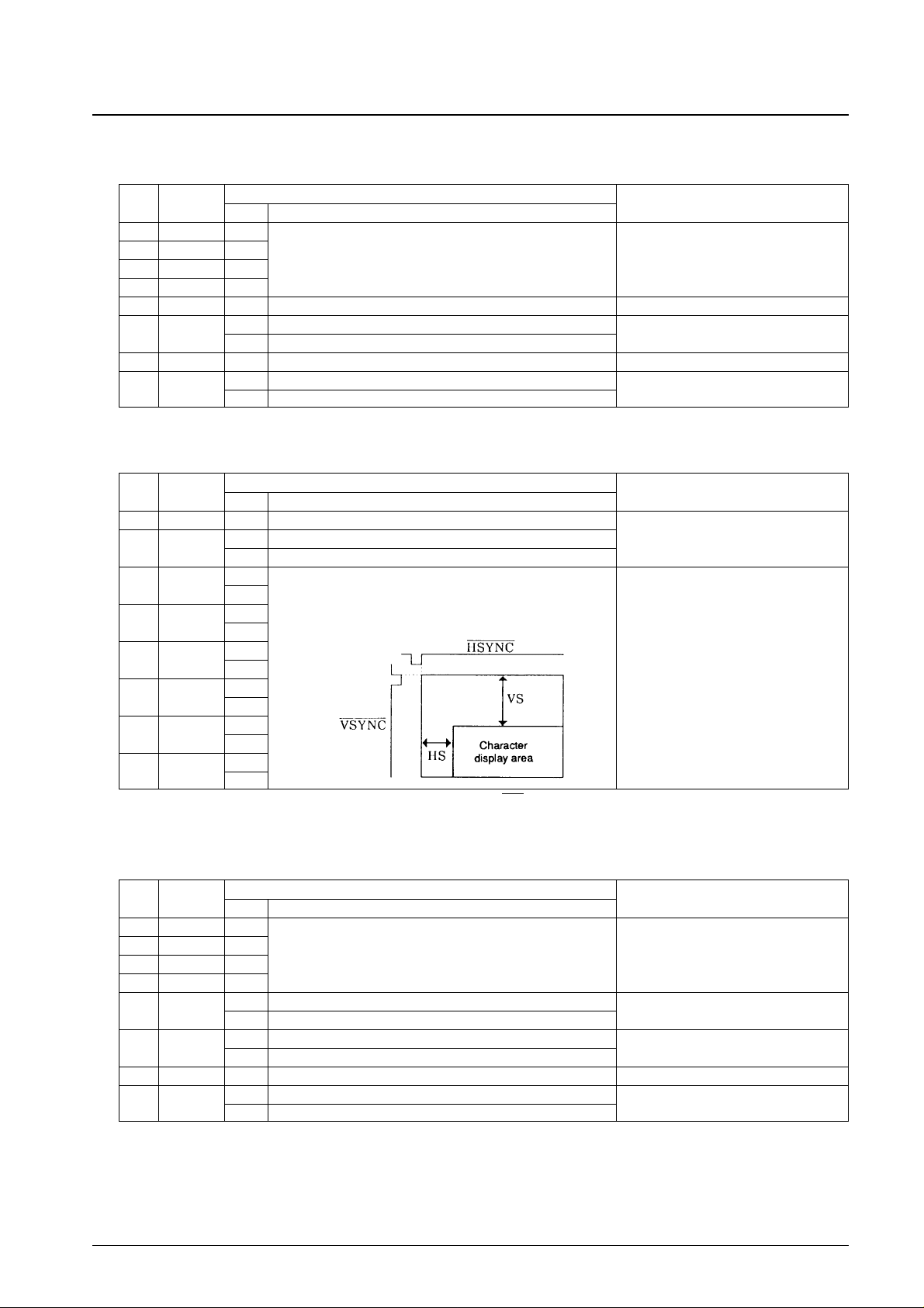
Display Screen Structure
The display consists of 24 characters × 10 rows for a maximum of 240 characters. The maximum number of characters is
reduced when the character size is enlarged.
Display memory addresses are specified as row (0 to 9 decimal) and column (0 to 23 decimal) addresses.
Display Screen Structure (display memory addresses)
No. 4841-10/12
LC74723, 74723M
DA Register
Contents
Note
0 to 7 name
State Function
7 — 1
6 — 1
Command 5 identification code
5 — 0
Synchronization signal control setup
4 — 1
3 — 0
0 Green background
Background color switching (Only valid in
2 PH NTSC mode, only a blue background color is
1 Blue background
supported in PAL-M mode.)
0 External synchronization signal detection control: Disabled
External synchronization signal detection
1 RSN
control Judges whether the signal has gone
1 External synchronization signal detection control: Enabled
from present to absent or from absent to
present.
0 INT
0 External synchronization
External/internal synchronization switching
1 Internal synchronization
Page 11

No. 4841-11/12
LC74723, 74723M
Composite Video Signal Output Level (internally generated level)
CV
OUT
output level waveform (VDD2 = 5.00 V)
Note: VDD2 = 5.00 V
Output level Output voltage ➀ [V] Output voltage ➁[V]
V
CHA
: Character 2.69 2.88
V
RSH
: Background color high 2.08 2.28
V
CBH
: Color burst high 1.72 1.91
V
RSL
: Background color low 1.56 1.75
V
BK1
: Trimming 2.13 2.30
V
BK0
: Trimming 1.55 1.73
V
PD
: Pedestal 1.40 1.59
V
CBL
: Color burst low 1.09 1.28
V
SN
: Sync 0.81 1.01
Page 12

No. 4841-12/12
LC74723, 74723M
This catalog provides information as of June, 1997. Specifications and information herein are subject to change
without notice.
■ No products described or contained herein are intended for use in surgical implants, life-support systems, aerospace
equipment, nuclear power control systems, vehicles, disaster/crime-prevention equipment and the like, the failure of
which may directly or indirectly cause injury, death or property loss.
■ Anyone purchasing any products described or contained herein for an above-mentioned use shall:
➀ Accept full responsibility and indemnify and defend SANYO ELECTRIC CO., LTD., its affiliates, subsidiaries and
distributors and all their officers and employees, jointly and severally, against any and all claims and litigation and all
damages, cost and expenses associated with such use:
➁ Not impose any responsibility for any fault or negligence which may be cited in any such claim or litigation on
SANYO ELECTRIC CO., LTD., its affiliates, subsidiaries and distributors or any of their officers and employees
jointly or severally.
■ Information (including circuit diagrams and circuit parameters) herein is for example only; it is not guaranteed for
volume production. SANYO believes information herein is accurate and reliable, but no guarantees are made or implied
regarding its use or any infringements of intellectual property rights or other rights of third parties.
 Loading...