

Page 1

Overview
The LC74411N and LC74411NE are digital processing
controllers for PIP (picture-in-picture) systems in TV sets
and VCRs. These ICs incorporate three circuits, a
multiplexed A/D converter, field memory, and a D/A
converter, to implement the PIP digital processing block in
a single chip.
Features
• Horizontal resolution: 450 pixels*
• Single-chip implementation of the three circuits required
in a PIP digital processing block: A/D converter, field
memory, and D/A converter circuits
• High image quality provided by vertical filtering
•I2C bus adopted
• Built-in PLL circuit (requires an external low-pass filter)
• Supports NTSC and PAL, TV and VCR applications,
and multi-format (NTSC and PAL) applications.
• External control function
• 8-bit D/A converter (PWM type): 6 pins
• General-purpose ports: 8 pins
• Sub-screen specifications
• Display on/off, frame/no frame, frame color switching,
wipe function
• Display position - Specifiable as an 8-bit value for each
of the horizontal and vertical directions.
• Size
Vertical reduction: 1/3, 1/4
Horizontal reduction: 1/3, 1/4
– The horizontal size can be adjusted by adjusting the
PLL divisor
– The display area vertical and horizontal positions
can be varied independently.
• Horizontal resolution (Y signal): about 190 dots
• Quantization: 6 bits
• Operating supply voltage LC74411NE : 5 V ±5%
LC74411N : 5 V ±10%
• Package
LC74411NE : QFP64E
LC74411N : DIP64S
Package Dimensions
unit: mm
3071-DIP64S
unit: mm
3159-QFP64E
CMOS LSI
Ordering number : EN*5519A
93196HA (OT) No. 5519-1/14
Preliminary
SANYO: DIP64S
[LC74411N]
SANYO: QIP64E
[LC74411NE]
SANYO Electric Co.,Ltd. Semiconductor Bussiness Headquarters
TOKYO OFFICE Tokyo Bldg., 1-10, 1 Chome, Ueno, Taito-ku, TOKYO, 110 JAPAN
PIP Controller
LC74411N, LC74411NE
Note:
When the main screen
synchronization PLL uses the
standard value
(PLL4 : 0 = 10110)
D/A clock
Y 11.6 MHz
R-Y 2.9 MHz
B-Y 2.9 MHz
Page 2
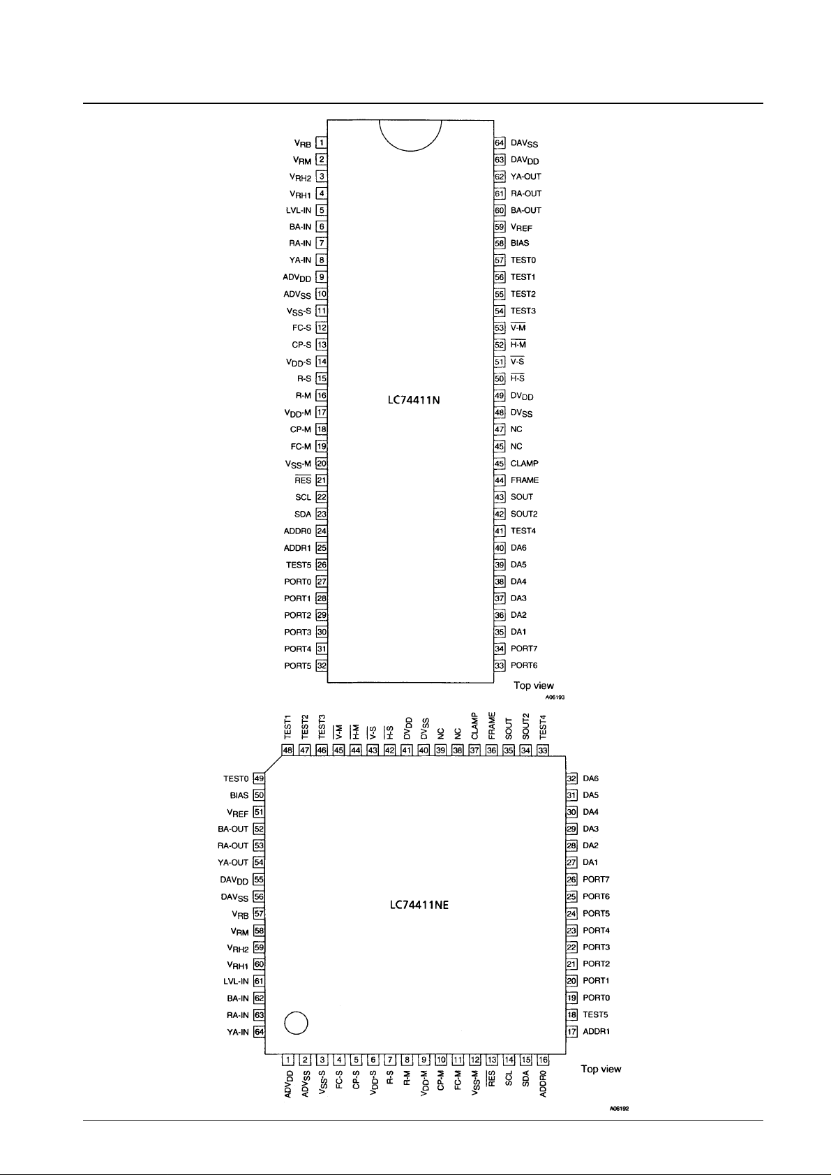
Pin Assignments
No. 5519-2/14
LC74411N, LC74411NE
Page 3

Block Diagram
No. 5519-3/14
LC74411N, LC74411NE
Page 4

LC74411N and LC74411NE Based PIP System
Function Overview
• Reduction sizes
– Vertical : 1/3, 1/4; The vertical filter coefficient can be selected.
– Horizontal: 1/3, 1/4; Variable at the PLL.
• Still image
– Field still image
• Display position
– Eight bits in each of the vertical and horizontal directions
• Frame
– Frame or no frame can be selected.
– Frame types differ according to the insertion method
Pin frame : A pin output that goes high at the frame position (for frame insertion by the application)
DAC frame: Frame overlapped onto the image signal. Four bits for each of the Y, R-Y, and B-Y signals.
• Wipe
– Supports eleven different types of wipe.
• Blanking size
– The vertical and horizontal directions can be specified independently (6 bits each)
– Eleven form specification types
• Memory clear
– The image data written to memory can be set to a fixed value.
– Either 25% white or blue can be selected.
• Wide-aspect-ratio TV support
– Aspect compensation function
• Support for NTSC, PAL, and multi-format systems
• External control function using the I2C bus
– Incorporates six on-chip 8-bit D/A converter circuits
– Provides eight general-purpose port pins.
• Wide range of settings and adjustments
– Sub-screen displacement, color shifting, and other settings can be adjusted using the I2C bus.
No. 5519-4/14
LC74411N, LC74411NE
Page 5

Sub-Screen Size
The vertical and horizontal directions can be controlled independently.
• Vertical size
– 1/3: Three scan lines are compressed to one.
– 1/4: Four scan lines are compressed to one.
• Horizontal size
– 1/3: A/D clock : D/A clock = 1:3
– 1/4: A/D clock : D/A clock = 1:4
When 1/4 compression is used, the output data will be 3/4 of 1/3 of the input data.
– Aspect ratio correction function
The horizontal size is adjusted by changing the VCO frequency (system clock).
This frequency can be changed from –30% to +30%.
Wipe Function
The WTOP, WBOT, WLEFT, and WRIGHT operations can be specified independently.
Display Area Function
This function controls an area to be blanked.
The vertical and horizontal directions can be set independently.
The operating mode is set using the wipe function WTOP, WBOT, WLEFT, and WRIGHT parameters.
No. 5519-5/14
LC74411N, LC74411NE
Page 6

Application Examples
• Exclusion of the masked area from a letterbox screen
• Small display
Minimizes the hidden sections of the main screen.
Internal Control Registers
0: These bits must be set to 0.
No. 5519-6/14
LC74411N, LC74411NE
Bit MSB LSB
Function
Address 7 6 5 4 3 2 1 0
00H SBY STL NT/PAL D-BLUE D-FIX FILD VDF-C0 POUT Mode settings
01H VP7 VP6 VP5 VP4 VP3 VP2 VP1 VP0 Vertical display position
02H HP7 HP6 HP5 HP4 HP3 HP2 HP1 HP0 Horizontal display position
03H 0 SIZE-V SIZE-H DAFRM YFC5 YFC4 YFC3 YFC2 Sub-screen size, frame color
04H RFC5 RFC4 RFC3 RFC2 BFC5 BFC4 BFC3 BFC2 Frame color
05H 0 0 0 PLL4 PLL3 PLL2 PLL1 PLL0 PLL value
06H PHP-M PHP-S WPE WP-MOD WTOP WBOT WLEFT WRIGHT Wipe
07H 0 0 VBS5 VBS4 VBS3 VBS2 VBS1 VBS0 Vertical display range
08H 0 0 HBS5 HBS4 HBS3 HBS2 HBS1 HBS0 Horizontal display range
09H V-BLK H-BLK CL-AJ1 CL-AJ0 WV-AJ1 WV-AJ0 WH-AJ1 WH-AJ0 Fine adjustment
0AH 0 YC-AJ2 YC-AJ1 YC-AJ0 YCFAJ1 YCFAJ0 FM-AJ1 FM-AJ0 Fine adjustment
0BH DAC1-7 DAC1-6 DAC1-5 DAC1-4 DAC1-3 DAC1-2 DAC1-1 DAC1-0 PWMDAC
0CH DAC2-7 DAC2-6 DAC2-5 DAC2-4 DAC2-3 DAC2-2 DAC2-1 DAC2-0 PWMDAC
0DH DAC3-7 DAC3-6 DAC3-5 DAC3-4 DAC3-3 DAC3-2 DAC3-1 DAC3-0 PWMDAC
0EH DAC4-7 DAC4-6 DAC4-5 DAC4-4 DAC4-3 DAC4-2 DAC4-1 DAC4-0 PWMDAC
0FH DAC5-7 DAC5-6 DAC5-5 DAC5-4 DAC5-3 DAC5-2 DAC5-1 DAC5-0 PWMDAC
10H DAC6-7 DAC6-6 DAC6-5 DAC6-4 DAC6-3 DAC6-2 DAC6-1 DAC6-0 PWMDAC
11H PORT7 PORT6 PORT5 PORT4 PORT3 PORT2 PORT1 PORT0 General-purpose ports
Page 7

Register Data Overview
No. 5519-7/14
LC74411N, LC74411NE
Address Register Notes
SBY Standby mode (The PLL circuit operates.)
STL Still image (Writes to internal memory are stopped.)
NT/PAL Format selection (H: NTSC, L:PAL)
00H
D-BLUE Memory clear data selection (Valid when D-FIX = 1) (H: blue, L: gray)
D-FIX Memory clear (Holds the data written to memory at a fixed value.)
FILD Field display selection
VDF-CO Vertical filter coefficient selection
POUT Sub-screen display on/off
01H VP7 to 0 Sub-screen vertical position
02H HP7 to 0 Sub-screen horizontal position
SIZE-V Vertical compression specification H: 1/4, L: 1/3
03H
SiZE-H Horizontal compression specification H: 1/4, L: 1/3
DAFRM D/A converter frame on/off
YFC5 to 2 D/A converter frame color (Y)
04H
RFC5 to 2 D/A converter frame color (R-Y)
BFC5 to 2 D/A converter frame color (B-Y)
05H PLL4 to 0 PLL divisor value (The standard value is 10110.)
PHP-M, S Field discrimination inversion/noninversion
06H
WPE Wipe or display area function enable
WP-MOD Wipe or display area function selection (H: wipe)
WTOP to WRIGHT Wipe or display area function format specification
07H VBS5 to 0 Display area range setting (vertical)
08H HBS5 to 0 Display area range setting (horizontal)
V-BLK, H-BLK D/A converter frame output range specification (Normally set to 00B)
09H
CL-AJ1, 0 A/D converter clamping potential adjustment (Can be monitored from the CLAMP pin.)
WV-AJ1, 0 Write vertical direction adjustment
WH-AJ1, 0 Write horizontal direction adjustment
YC-AJ2 to 0 C phase (with respect to Y) adjustment
0AH YCFAJ1, 0 D/A converter frame C phase (with respect to Y) adjustment
FM-AJ1, 0 D/A converter frame left/right width adjustment
0BH DAC1-7 to 0 External control D/A converter (8-bit PWM) data
0CH DAC2-7 to 0 External control D/A converter (8-bit PWM) data
0DH DAC3-7 to 0 External control D/A converter (8-bit PWM) data
0EH DAC4-7 to 0 External control D/A converter (8-bit PWM) data
0FH DAC5-7 to 0 External control D/A converter (8-bit PWM) data
10H DAC6-7 to 0 External control D/A converter (8-bit PWM) data
11H PORT7 to 0 Data for the general-purpose output ports
Page 8

Pin Functions
Notes:The 64E pin numbers refer to the LC74411NE and the 64S pin numbers refer to the LC74411N.
The letter "S" in an inverter indicates Schmitt input characteristics.
No. 5519-8/14
LC74411N, LC74411NE
Pin No.
Pin I/O Connection Function Circuit type
64E 64S
13 21 RES I Initialization circuit Reset
45 53 V-M I Main screen vertical synchronizing signal (negative polarity)
44 52 H-M I Synchronization separation Main screen horizontal synchronizing signal (negative polarity)
43 51 V-S I circuit IC Sub-screen vertical synchronizing signal (negative polarity)
42 50 H-S I Sub-screen horizontal synchronizing signal (negative polarity)
14 22 SCL I Microcontroller Serial clock
15 23 SDA I/O Microcontroller Serial data
16 24 ADDR0 I DV
SS
Must be connected to VSSin normal operation.
17 25 ADDR1 I DV
SS
19 27 PORT0 O
20 28 PORT1 O
21 29 PORT2 O
22 30 PORT3 O
General-purpose ports
23 31 PORT4 O
24 32 PORT5 O
25 33 PORT6 O
26 34 PORT7 O
27 35 D/A1 O
28 36 D/A2 O
29 37 D/A3 O
PWM D/A converter outputs
30 38 D/A4 O
31 39 D/A5 O
32 D/A6 O
36 44 FRAME O Analog circuits Frame pulse output
35 43 SOUT O Analog circuits Main/sub-screen switching signal
34 42 SOUT2 O
38 46 NC No connection
39 47 NC No connection
41 49 DV
DD
Power supply Digital system power supply
40 48 DV
SS
Ground Digital system power supply
64 8 YA-IN I Analog circuits Sub-screen analog input (Y)
63 7 RA-IN I Analog circuits Sub-screen analog input (R-Y)
62 6 BA-IN I Analog circuits Sub-screen analog input (B-Y)
61 5 LVL-IN I Preset voltage
37 45 CLAMP O A/D converter clamp pulse
For use by user monitoring circuits
Continued on next page.
Page 9

No. 5519-9/14
LC74411N, LC74411NE
Pin No.
Pin I/O Connection Function Circuit type
64E 64S
60 4 V
RH1
Power supply or VRH2 Low-pass filter
59 3 V
RH2
Open or VRH1 Low-pass filter
58 2 V
RM
Capacitor Oscillator range setting resistor
57 1 V
RB
Capacitor and V
REF
Power supply
1 9 ADV
DD
Power supply Ground
2 10 ADV
SS
Ground
54 62 YA-OUT O Analog circuits Sub-screen digital analog output (Y)
53 61 RA-OUT O Analog circuits Sub-screen digital analog output (R-Y)
52 60 BA-OUT O Analog circuits Sub-screen digital analog output (B-Y)
51 59 V
REF
I VRB D/A converter analog setting pin
50 58 BIAS — Capacitor
55 63 DAV
DD
Power supply Analog system power supply (D/A converter)
56 64 DAV
SS
Ground
10 18 CP-M O Low-pass filter Charge pump output
11 19 FC-M I Low-pass filter Oscillator control voltage input
8 16 R-M — Oscillator range setting
resistor
9 17 V
DD
-M Power supply VCO power supply
12 20 V
SS
-M Ground
5 13 CP-S O Low-pass filter Charge pump output
4 12 FC-S I Low-pass filter Oscillator control voltage input
7 15 R-S — Oscillator range setting resistor
6 14 V
DD
-S Power supply VCO power supply
3 11 V
SS
-S Ground
49 57 TEST0 I
48 56 TEST1 I
47 55 TEST2 I
DV
SS
Testing (These pins must connected to DVSS.)
46 54 TEST3 I
33 41 TEST4 I
18 26 TEST5 I
Parameter Symbol Conditions Ratings Unit
Maximum supply voltage V
DD
max –0.3 to +7.0 V
Maximum input voltage V
IN
max –0.3 to V
DD
+0.3 V
Maximum output voltage V
OUT
max –0.3 to V
DD
+0.3 V
Allowable power dissipation Pd max
LC74411NE 550 mW
LC74411N 600 mW
Operating temperature Topr –10 to +70 °C
Storage temperature Tstg –55 to +125 °C
Specifications
Absolute Maximum Ratings at Ta = 25 ±2°C, VSS= 0 V
Allowable Operating Ranges at Ta = –10 to +70°C, VSS= 0 V
Parameter Symbol Conditions min typ max Unit
Supply voltage V
DD
LC74411NE 4.75 5.0 5.25 V
LC74411N 4.5 5.0 5.5 V
Digital input high-level voltage V
IH
0.7V
DD
V
Digital input low-level voltage V
IL
0.3V
DD
V
Analog input voltage
The YA-IN, RA-IN, and BA-IN pins
ADVDD-V
RB
Vp-p
Reference voltage V
REF
2.7 0.8V
DD
V
DD
V
Continued from preceding page.
Page 10

No. 5519-10/14
LC74411N, LC74411NE
Electrical Characteristics at Ta = 25 ±2°C, VDD= 5 V ±5% (LC74411NE), VDD= 5 V ±10% (LC74411N), VSS= 0 V
Parameter Symbol Conditions min typ max Unit
Output high-level voltage
V
OH1
IOH= –1 mA, the CP-M and CP-S pins VDD–1 V
V
OH2
IOH= –1 mA, pins other than CP-M and CP-S VDD–1 V
V
OL1
IOL= 1 mA, the CP-M and CP-S pins 1.0 V
Output low-level voltage V
OL2
IOL= 3 mA, the SDA pin 0.4 V
V
OL3
IOL= 2 mA, pins other than the pins mentioned above 0.4 V
Quiescent current drain I
DD
ST RES = VSS, DC pin inputs, no output loads 10 µA
Reference voltage (M) V
RM
When V
RH1
is connected to ADV
DD
0.9V
DD
V
Reference voltage (B) V
RB
When V
RH1
is connected to ADV
DD
0.8V
DD
V
Input leakage current I
LK
VI= VDD, V
SS
–1 +1 µA
Output leakage current I
OZ
VI= V
DD,VSS
; the CP-M and CP-S pins –1 +1 µA
D/A converter output resistance R
DA
300 Ω
Switching Characteristics at Ta = 25 ±2°C, VDD= 5 V ±5% (LC74411NE), VDD= 5 V ±10% (LC74411N), VSS= 0 V
Parameter Symbol Conditions min typ max Unit
Vertical synchronizing signal
Pulse width t
VW
1 µs
Rise time t
VR
300 ns
Fall time t
VF
300 ns
Horizontal synchronizing signal
Pulse width t
HW
1 µs
Rise time t
HR
300 ns
Fall time t
HF
300 ns
I
2
C timing
SCL frequency t
SCL
100 kHz
Bus release time t
BUF
4.7 µs
Start/hold t
HD STA
4.0 µs
SCL low period t
LOW
4.7 µs
SCL high period t
HIGH
4.0 µs
Data hold time t
HD DAT
0 µs
Data setup time t
SU DAT
250 ns
Rise time t
R
1000 ns
Fall time t
F
300 ns
Stop setup time t
SU STO
4.0 µs
Page 11

Sub-Screen Digital Processing Specifications
No. 5519-11/14
LC74411N, LC74411NE
Item NTSC (fH= 15734Hz) PAL (fH= 15625Hz)
Order Y, R–Y, Y, B–Y, Y, –, Y, –, ······
Frequency 480 f
H
fT(MHz) 7.552 7.500
Y only 240 f
H
A/D converter sampling f
TY
3.776 3.750
R-Y only 60 f
H
f
TR
0.944 0.938
B-Y only 60 f
H
f
TB
0.944 0.938
Number of bits in quantization 6 bits
Y signal 736 f
H
f
CY
11.58 11.50
D/A converter clock R-Y signal 184 f
H
(MHz)*1 f
CR
2.895 2.875
B-Y signal 184 f
H
f
CB
2.895 2.875
Number of horizontal bits 288
Y only 192
Write R-Y only 48
B-Y only 48
Number of vertical lines 73 85
Number of horizontal bits 268
Y only 180
Readout display*2
R-Y only 44
B-Y only 44
Number of vertical lines 72 84
Note: 1. When the PLL divisor has its standard value (PLL4:0 = 10110).
2. Target values are shown. (The number of horizontal bits varies with, for example, the frame width adjustment.)
Initialization
(1) RES pin: Reset
The RES pin must be held low when power is first applied with the timing shown in the figure.
(2) Internal control registers
After a reset, the chip goes to the standby state (SBY = high). When developing the microcontroller software, that
software must be designed so that it transmits data for all registers. Also note that data values of zero (0) must be sent
for the control registers that have ‘0’ entries in the control register table.
Page 12

I2C Control
Data format
Data 1 is stored at register address A1. Data 2 is stored at register address A1 + 1, i.e., the address given by incrementing
A1. If the address exceeds 11H, it wraps to 00H.
Slave address:
Synchronizing Signal Input
• Sync separation
The LC74411N and LC74411NE require sync separated (including AFC processing) V and H signals for both the main
and sub-screen. Since V is used for field discrimination and H is used as the PLL reference signal, these signals must be
provided reliably.
– The H-M and H-S pin inputs are assumed to be delayed about 1 µs from the video signal’s horizontal synchronizing
signal and set to standard values.
– Equalizing pulses must be excluded.
– Since noise on the synchronizing signal will disrupt the display, these lines should be placed carefully.
– If the synchronizing signal is unstable, the sub-screen display may be disrupted. We recommend turning off sub-
screen display in such cases.
• Field discrimination circuit
Since the circuit discriminates based on the phase difference between the falling edges of the H and L signals, these
signals must be provided with the timing shown in the figure below.
No. 5519-12/14
LC74411N, LC74411NE
A6 A5 A4 A3 A2 A1 A0 R/W
0 0 1 0 0 1 1 0
Page 13

Clamp Pulses
• A/D converter clamping
Since clamp pulses are output to the built-in A/D converter with the timing shown in the figure below, they are set up to
fall in the pedestal range. The clamp pulses can be monitored at the CLAMP pin. On a reset or in standby mode, the
H-S input signal becomes positive polarity and is output without change.
• D/A converter clamp
External Control Output Blanking
No. 5519-13/14
LC74411N, LC74411NE
Page 14

No. 5519-14/14
LC74411N, LC74411NE
This catalog provides information as of September, 1996. Specifications and information herein are subject to
change without notice.
■ No products described or contained herein are intended for use in surgical implants, life-support systems, aerospace
equipment, nuclear power control systems, vehicles, disaster/crime-prevention equipment and the like, the failure of
which may directly or indirectly cause injury, death or property loss.
■ Anyone purchasing any products described or contained herein for an above-mentioned use shall:
➀
Accept full responsibility and indemnify and defend SANYO ELECTRIC CO., LTD., its affiliates, subsidiaries and
distributors and all their officers and employees, jointly and severally, against any and all claims and litigation and all
damages, cost and expenses associated with such use:
➁
Not impose any responsibility for any fault or negligence which may be cited in any such claim or litigation on
SANYO ELECTRIC CO., LTD., its affiliates, subsidiaries and distributors or any of their officers and employees
jointly or severally.
■ Information (including circuit diagrams and circuit parameters) herein is for example only; it is not guaranteed for
volume production. SANYO believes information herein is accurate and reliable, but no guarantees are made or implied
regarding its use or any infringements of intellectual property rights or other rights of third parties.
 Loading...