

Page 1

Ordering number :EN *5684
22897HA (OT) No. 5684-1/21
Overview
The LC74201E is a CMOS LSI that reduces the signal
processing functions required of a video CD decoder to a
single chip. All that it takes to make a version 1 or version
2 video CD player is the addition of a CD digital signal
processor, DRAM, an audio D/A converter, digital video
encoder, and similar components.
Features
• Incorporation of virtually almost all the functionality
required by a video CD player from the CD-ROM
decoder through to the MPEG audio and video decoders
in a single chip
• Fully automatic playback with automatic decoding
within the LSI in response to simple external commands
and the MPEG bit stream
• Special playback functions are activated by command
inputs, and do not require signal processing by the host
microcomputer
• Support for two external DRAM configurations:
4 M bits (256k × 16 bits) or 4 M bits (256k × 16 bits) +
1 M bit (64k × 16 bits)
• Support for a Track 1 DRAM user area (i.e., sector
buffer) of up to 8 k bytes (4 M bits of external DRAM)
or 22 k bytes (5 M bits of external DRAM)
• Automatic synchronization of audio and video
• Built-in high-speed decoder core that supports variablespeed video playback at up to quadruple speed. Audio
support for normal and double-speed playback.
• Internal registers that offer configuration settings for
connecting to most commercially available CD digital
signal processors and D/A converters
• Compatible with version 2 of the video CD standard.
Support for superimposition of closed caption data on
the output signal as specified in the EIA608 standard
• Support for Photo CD standard. (Base/4 and Base/16)
Package Dimensions
unit: mm
3182-QFP-128E
Preliminary
SANYO: QIP-128E
[LC74201E]
LC74201E
SANYO Electric Co.,Ltd. Semiconductor Bussiness Headquarters
TOKYO OFFICE Tokyo Bldg., 1-10, 1 Chome, Ueno, Taito-ku, TOKYO, 110 JAPAN
Video CD Decoder
CMOS LSI
Page 2

Pin Assignment
No. 5684-2/21
LC74201E
Page 3
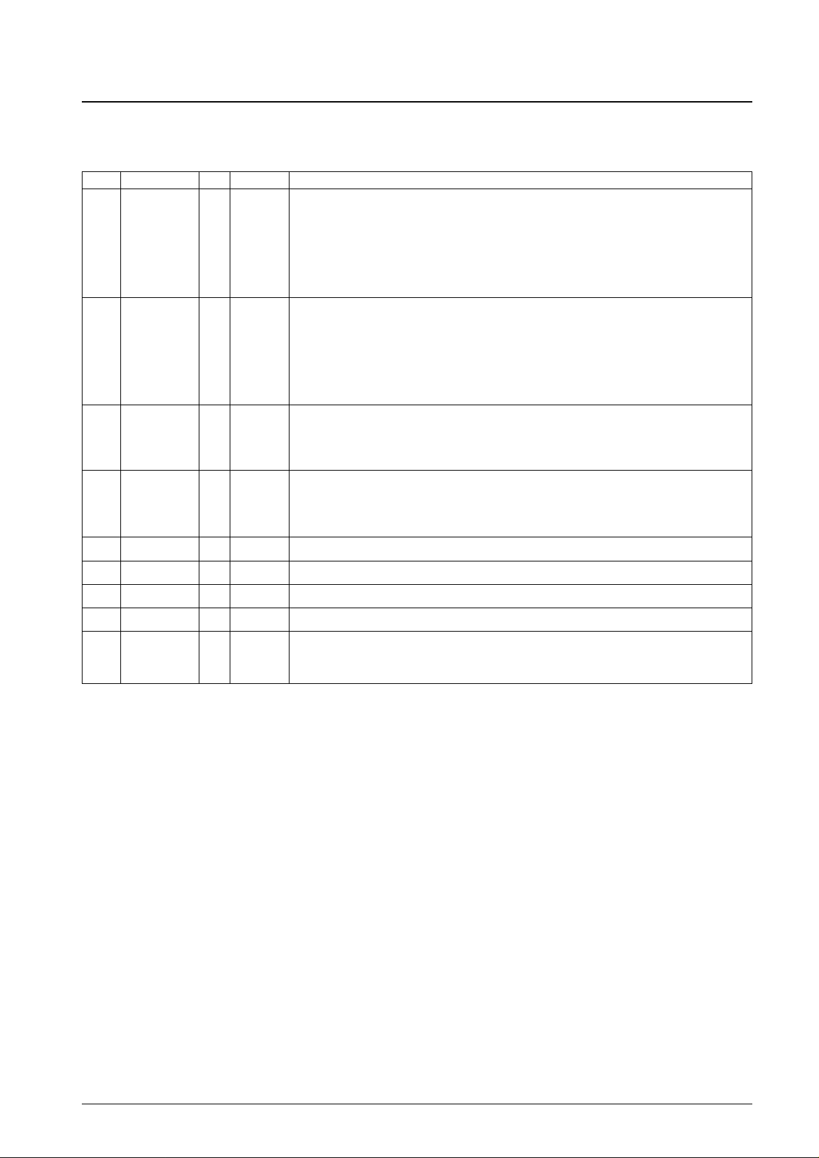
Pin Function
1. Power supply, test pin, unconnected pins
No. 5684-3/21
LC74201E
Pin No. Symbol I/O Logic Function
17
39
60
75
81
124
DV
DD
1
– – System power supply (3-V power supply: 3.7 to 4.0 V)
20
37
54
69
76
105
DV
SS
1
– – System power supply (connect to ground)
29
114
DV
DD
2
– – Power supply for 5-V I/O pins (5-V power supply: 5.5 ± 0.5 V)
33
112
DV
SS
2
– – Power supply for 5-V I/O pins (connect to ground)
NC – –
Unconnected pins
34, 36, 40, 42, 53, 57, 64, 82, 83, 84 pins
85, 86, 97, 98, 108, 110, 126, 128 pins
65
AV
SS
– – Power supply for VCO and PLL (connect to ground)
67
AV
DD
– – Power supply for VCO and PLL (3-V power supply: 3.7 to 4.0 V)
125 CLKO Out Positive Power supply for VCO and PLL (connect to ground)
127 TEST In Positive Test mode control pin (normally kept at low level)
Page 4

2. Clock pins
3. Microcomputer interface
Note: AD0 to AD7 use N-channel open-drain outputs.
No. 5684-4/21
LC74201E
Pin No. Symbol I/O Logic Function
18 FSCO Out Positive
Subcarrier clock output (frequency = 1/4 pixel clock frequency). Tristate output using DV
DD
2 (5-V) power
supply.
19 PCKO Out Positive
Pixel clock output (NTSC-4fsc, PAL-4fsc, or 13.5 MHz). Tristate output using DV
DD
1 (3-V) power supply.
61 CLKSEL In Positive
Clock selection control input. High: 54.0-MHz clock input from pin 62 (CLKIN); Low: clock from internal
VCO oscillator.
62 CLKIN In Positive
54.0-MHz clock input (with built-in bias). When not used, connect to DV
DD
1 or DVSS1.
55 XPALIN In –
Crystal oscillator connections for PAL-4fsc oscillation circuit (4fsc = 17.734475 MHz)
58 XNTIN In –
Crystal oscillator connections for NTSC-4fsc oscillation circuit (4fsc = 14.31818 MHz)
56 XPALOUT Out –
56 –
59 XNTOUT Out –
66 PLLFIL – – PLL filter connection
CD-DSP clock input (16.9344, 2.8224, or 2.1168 MHz)
Adjustment resistor connection for VCO oscillator circuit.63 VCOR – –
68 CDCK In Positive
Pin No. Symbol I/O Logic Function
44 STB (CL) In Positive
Parallel interface: Strobe signal input for address input and data I/O.
Serial interface: Serial transfer clock signal input.
45 AD0 (DO) I/O Positive
Parallel interface: Address/data I/O port P0 (LSB).
Serial interface: ZPSerial data output (LSB-first input).
43 AS/DS (CE) In Positive
Parallel interface: Address/data select input (Low = address).
Serial interface: Serial transfer enable signal input (High = enabled).
46 AD1 (DI) I/O Positive
Parallel interface: Address/data I/O port P1.
Serial interface: Serial data input (LSB-first output).
41 IRQ Out Negative Interrupt request signal output (N-channel open-drain output).
Parallel interface address/data I/O ports.
The interface mode is determined by the input levels at the AD4 to AD6 pins at the rising edge of the
RESET pin input.
• Serial interface: AD6:AD5:AD4 = 1:*:* (* = Don’t care)
• Parallel interface: AD6:AD5:AD4 = 0:1:0
AD7: Parallel interface address/data I/O port P7 (MSB).
System reset input (Hysteresis input; built-in pull-up resistor).
38 REST In Negative
47 AD2 I/O Positive
48 AD3 I/O Positive
49 AD4 I/O Positive
50 AD5 I/O Positive
51 AD6 I/O Positive
52 AD7 (MBS) I/O Positive
Page 5
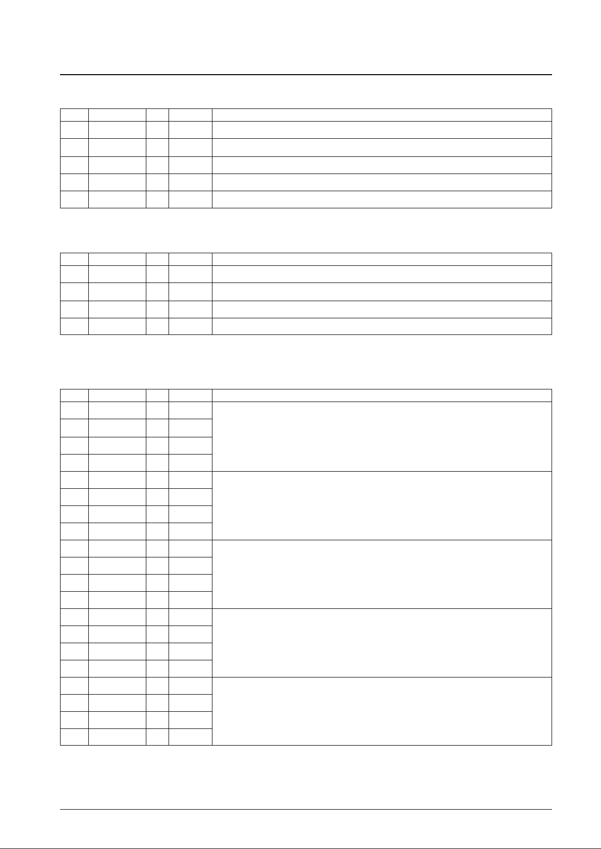
4. CD interfaces
5. Audio D/A converter interface
Note:The four pins making up the audio D/A converter interface all use N-channel open-drain outputs.
6. Video interface
No. 5684-5/21
LC74201E
Pin No. Symbol I/O Logic Function
71 CDC2P In Positive C2 error flag input (hysteresis input)
Emphasis input (hysteresis input)70 CDEMPH In Positive
73 CDBCK In Positive Serial data bit clock input (hysteresis input)
Serial data input (hysteresis input)72 CDSD In Positive
Left/right clock input (hysteresis input)74 CDLRCK In Positive
Pin No. Symbol I/O Logic Function
2 BV1 I/O Positive
Video signal outputs (B/V signals). (Inputs only in test mode.)
1 BV0 (LSB) I/O Positive
4 BV3 I/O Positive
3 BV2 I/O Positive
Video signal outputs (B/V signals). (Inputs only in test mode.)
Tristate output using DV
DD
1 (3-V) power supply.
5 BV4 I/O Positive
7 BV6 I/O Positive
6 BV5 I/O Positive
9 GU0 (LSB) I/O Positive Video signal outputs (G/U signals). (Inputs only in test mode.)
Tristate output using DV
DD
2 (5-V) power supply.
8 BV7 (MSB) I/O Positive
10 GU1 I/O Positive
12 GU3 I/O Positive
Tristate output using DV
DD
1 (3-V) power supply.
11 GU2 I/O Positive
14 GU5 I/O Positive
Video signal outputs (G/U signals). (Inputs only in test mode.) 13 GU4 I/O Positive
15 GU6 I/O Positive
21 RY0 (LSB) I/O Positive Video signal outputs (R/Y signals). (Inputs only in test mode.)
Tristate output using DV
DD
2 (5-V) power supply.
16 GU7 (MSB) I/O Positive
23 RY2 I/O Positive
22 RY1 I/O Positive
Tristate output using DV
DD
1 (3-V) power supply.
24 RY3 I/O Positive
Pin No. Symbol I/O Logic Function
78 AUEMPH Out Positive Audio emphasis flag output
Audio data left/right clock output77 AULRCK Out Positive
80 AUBCO Out Positive Audio data bit clock output
Audio data serial output79 AUDOUT Out Positive
Continued on next page.
Page 6

Continued from preceding page
No. 5684-6/21
LC74201E
Pin No. Symbol I/O Logic Function
26 RY5 I/O Positive
Video signal outputs (R/Y signals). (Inputs only in test mode.)
25 RY4 I/O Positive
28 RY7 (MSB) I/O Positive
27 RY6 I/O Positive
Horizontal synchronization signal output. Tristate output using DV
DD
2 (5-V) power supply.
Composite synchronization signal output. Tristate output using DVDD2 (5-V) power supply.
Blanking signal output (horizontal and vertical blanking interval signal). Tristate output using DV
DD
2 (5-V)
power supply.
Tristate output using DV
DD
2 (5-V) power supply.
30 HSYNC Out Negative
32 BLANK Out Positive
31 CSYNC Out Negative
35 VOE In Positive Video output enable signal input. High: Enable output.
87 DD15 (MSB) I/O Positive
89 DD13 I/O Positive
Data bus to DRAM.
Tristate output using DV
DD
2 (5-V) power supply.
Row address strobe signal output to expansion 1-Mbit DRAM.
Tristate output using DV
DD
2 (5-V) power supply.
7
Write enable signal output to DRAM. Tristate output using DV
DD
2 (5-V) power supply.
Column address strobe signal output to DRAM. Tristate output using DV
DD
2 (5-V) power supply.
88 DD14 I/O Positive
91 DD11 I/O Positive
90 DD12 I/O Positive
92 DD10 I/O Positive
94 DD8 I/O Positive
93 DD9 I/O Positive
96 DD6 I/O Positive
95 DD7 I/O Positive
99 DD5 I/O Positive
101 DD3 I/O Positive
100 DD4 I/O Positive
103 DD1 I/O Positive
102 DD2 I/O Positive
104 DD0 (LSB) I/O Positive
107 RAS0 Out Positive
106 RAS1 Out Positive
111 CAS Out Positive
109 WE Out Positive
Output enable signal output to DRAM. Tristate output using DV
DD
2 (5-V) power supply.
113
OE
Out Positive
Continued on next page.
Page 7

Continued from preceding page
Block Diagram
Pin No. Symbol I/O Logic Function
116 AA7 Out Positive
Address output to DRAM.
115 AA8 (MSB) Out Positive
118 AA5 Out Positive
117 AA6 Out Positive
119 AA4 Out Positive
121 AA2 Out Positive
Tristate output using DV
DD
2 (5-V) power supply.
120 AA3 Out Positive
123 AA0 (LSB) Out Positive
122 AA1 Out Positive
No. 5684-7/21
LC74201E
Page 8

Block Descriptions
1. CD-ROM decoder
This block takes the MPEG bit stream from the external CD digital signal processor and decodes it in accordance
with the CD-ROM standard.
• The decoded data is automatically transferred to the next stage, the system decoder.
• Storing the decoded data in DRAM is also possible.
• The high-speed decoder core supports quadruple-speed playback.
• Internal registers offer settings for connecting to most commercially available CD digital signal processors.
— 32- or 24-slot
— LSB or MSB first
— Front- or rear-packing for data
— Rising or falling edge for bit clock
• The video CD’s track 1 data can be stored in a user area set aside in the external DRAM.
• An auto restart function stores the address of the last sector accessed before a pause so that playback can resume at
the next sector when the pause ends.
• The contents of the sector header and subheader are available from registers.
2. System decoder
This block analyzes the MPEG bit stream, splits it into video and audio bit streams, and transfers these bit streams to
the corresponding decoders. It calculates the decode start timing from the time stamp and the decoders’ inherent
delays and generates the necessary start signals to provide automatic synchronization of audio and video outputs.
3. CPU interface
This interface allows the CPU to access the internal registers to set parameters controlling operation and to read out
operational status. It may be configured as either an 8-bit parallel interface multiplexing data and addresses or as a
4-wire serial interface.
4. Audio decoder
This block decodes the MPEG1 audio bit stream from the system decoder in accordance with the ISO11172-3
standard.
• The use of 24-bit internal precision yields high audio quality.
• The decoder supports all MPEG audio modes defined for layers 1 and 2 except the free format mode.
• Internal registers offer settings for connecting to most commercially available D/A converters.
• The block includes a cross attenuator compliant with the CD-i standard.
• The block supports readout of the frame header data.
• The block performs CRC checking. If there is an error, it automatically substitutes the preceding frame stored in
DRAM. If there are continuous errors, it switches to muting.
Cross Attenuator
No. 5684-8/21
LC74201E
Page 9

5. Video decoder
This block decodes all layers (from the video sequence layer to the block layer plus the headers) from the MPEG1
video bit stream from the system decoder in accordance with the ISO11172-2 standard.
• The decoding requires no external signal processing. The LSI internals handle everything automatically. All that is
required from outside the chip are simple commands and the MPEG bit stream.
• A PLL circuit permits synchronization of the system clock with the CD digital signal processor. Commands offer a
choice of the following frequencies.
— 16.9344 MHz
— 2.8224 MHz
— 2.1168 MHz
• The decoder supports the following image formats.
— 352 dots × 240 lines, 29.97 Hz (NTSC, PAL-60 Hz)
— 352 dots × 240 lines, 23.976 Hz (Film)
— 352 dots × 288 lines, 25.00 Hz (PAL)
— 704 dots × 480 lines, high-resolution still image (NTSC)
— 704 dots × 576 lines, high-resolution still image (PAL)
• Built-in filters provide high image quality.
— Built-in sampling rate conversion filter for horizontal direction
— Built-in vertical filter
• The decoder supports a variety of video output specifications.
— Support for NTSC (59.94 Hz) and PAL (50 Hz) monitors
— Built-in video timing generator
— Switching between interlaced and non-interlaced operation
— Built-in YUV-to-RGB conversion matrix with choice of 24-bit RGB, 24-bit YUV, and 16-bit YUV output
— Film-NTSC conversion
— Simple two-way conversion between NTSC or Film and PAL with built-in aspect ratio conversion
— Choice of pixel clocks: 13.5 MHz, 6.75 MHz, and 4 fsc
• The decoder offers special playback functions.
— Special playback functions require no signal processing by the CPU.
— Such functions as double-, triple-, and quadruple-speed playback, still image playback, pause, slow, and single-
stepping (one-cut play) are available with simple commands.
— The built-in multitile function offers the display of 4 or 16 small images on the screen with the display
positions freely selectable and processing of up to two fields supported.
— The built-in wipe function supports wiping within a frame, display outside that frame, and changing the frame
color.
• The decoder includes bit buffer management functions.
— These monitor the bit buffer for errors and control the decoder to automatically adjust the amount of data in the
bit buffer to maintain normal operation at all times.
— Depending on the state of the bit buffer, the decoder automatically skips or repeats images. Skipping gives
precedence to B pictures.
• The decoder includes frame buffer management functions. These provide all internal support for frame buffer
mapping control (for the display, reconstruction frame,front frame, and rear frame) and the mapping control and
setting accompanying mode changes between high-resolution still images and motion picture playback.
• The decoder includes various fail-safe functions.
• The decoder supports version 2 of the video CD standard.
— User data is accessible from outside the decoder.
— The decoder supports superimposition of closed caption data on the output RGB/YUV signal as specified in the
EIA608 standard.
• The decoder supports decoding of Photo CDs (using Base/4 and lower).
No. 5684-9/21
LC74201E
Page 10

6. DRAM arbiter
This block provides the interface to the external DRAM. In addition to the standard 4-M bit DRAM, there can also
be a 1-M bit DRAM for supporting PAL high-resolution still image playback. If this additional DRAM is not
available, the LSI trims the top and bottom 48 lines of the image and provides a function for vertically scrolling the
display area in 16-line increments.
No. 5684-10/21
LC74201E
Page 11

Absolute Maximum Ratings
Recommended Operating Conditions at Ta = –25°C to +75°C
No. 5684-11/21
LC74201E
Parameter Symbol Conditions
Ratings
Unit
min max
V
DD
1 DVDD1 pin DVSS1 – 0.3 DVSS1 + 4.0 V
Power supply voltage V
DD
2 DVDD2 pin DVSS2 – 0.3 DVSS2 + 6.0 V
V
DD
3 AVDDpin AVSS– 0.3 AVSS+ 4.0 V
BV0 to EV3, GU0 to GU3, RY0 to RY3,
V
IN
1 RESET, XPALIN, XNTIN, CLKIN, VCOR, DVSS1 – 0.3 DVDD1 + 0.3 V
PLLFIL, TEST pins
VOE, AS/DS, STB, AD0 to AD7, CLKSEL
Input voltage V
IN
2 CDCK, CDEMPH, CDC2P, CDSD, CDBCK, DVSS1 – 0.3 5.5 V
CDLRCK pins
V
IN
3
BV4 to BV7, GU4 to GU7, RY4 to TY7,
DVSS2 – 0.3 DVSS2 + 0.3 V
DD0 to DD15 pins
BV0 to EV3, GU0 to GU3, RY0 to RY3,
V
OUT
PCK0, XPALOUT, XNTOUT, CLK0, AULRCK, DVSS1 – 0.3 DVDD1 + 0.3 V
AUEMPH, AUDOUT, AUBC0 pins
Output voltage V
OUT
IRQ, AD0 to AD 7, CAS pins DVSS1 – 0.3 – V
BV4 to BV7, GU4 to GU7, RY4 to TY7,
V
OUT
FSC0, HSYNC, CSYNC, BLANK, RAS0, RAS1, DVSS2 – 0.3 DVSS2 + 0.3 V
WE, OE, AA0 to AA8 pins
Maximum current drain Pd max Ta = 25°C – 500 mW
Operating temperature Topr –25 +75 °C
Storage temperature Tstg –40 +125 °C
Parameter Symbol Conditions
Ratings
Unit
min typ max
V
DD
1 DV
DD1
pin 3.7 – 4.0 V
Supply voltage V
DD
2 DV
DD2
pin 4.5 5.0 5.5 V
V
DD
3 AVDDpin 3.7 – 4.0 V
V
IH
1 BV0 to BV3, GU0 to GU3,RY0 to RY3 pins 0.7VDD1 – VDD1 + 0.3 V
V
IH
2 RESET pin 0.8VDD1 – VDD1 + 0.3 V
V
IH
3 VOE, AD0 to AD7, CDCK, CLKSEL, TEST pins 0.7VDD1 – 5.5 V
High-level input voltage
V
IH
4
AS/DS, STB, CDEMPH, CDC2P, CDSD, CDBCK,
CDLRCK pins
0.8V
DD
1 – 5.5 V
V
IH
5
BV4 to BV7, GU4 to GU7, RY4 to RY7,
DD0 to DD15 pins
0.7V
DD
1 – VDD2 + 0.3 V
V
IL
1
BV0 to BV7, GU0 to GU7, RY0 to RY7, VOE, CDCK,
Low-level input voltage
AD0 to AD7, CLKSEL, TEST, DD0 to DD15 pins
V
SS
1 – 0.3 – 0.3VDD1 V
V
IL
2
RESET, AS/DS, STB, CDEMPH, CDC2P,CDSD,
CDBCK, CDLRCK pins
V
SS
1 – 0.3 – 0.2VDD1 V
Clock frequency
FOSC1 XPALIN, XPALOUT pins (PAL) – 17.734475 – MHz
FOSC2 XNTIN, XNTOUT pins (NTSC) – 14.31818 – MHz
Input amplitude V
IN
1 CLKIN pin (CLKSEL = high; FIN2 = 54 MHz) 1.0 – VDD1 + 0.3 Vp-p
Command – 11hex; D1, D0 = 0,0 – 16.9344 – MHz
Input frequency
F
IN
1 CDCK pin Command – 11hex; D1, D0 = 0,1 – 2.1168 – MHz
Command – 11hex; D1, D0 = 1,0 – 2.8224 – MHz
F
IN
2 CLKIN pin (CLKSEL = high) – 54.000 – MHz
Clock duty fduty CLKIN, CDCK pins 40 – 60 %
Page 12

Electrical Characteristics
at Ta = –25 to +75°C, DVDD1 = AVDD= 3.7 V and DVDD2 = 5.0 V unless otherwise specified.
No. 5684-12/21
LC74201E
Parameter Symbol Conditions
Ratings
Unit
min typ max
I
IH
1
AS/DS, STB, CDEMPH, CDC2P,CDSD, CDBCK,
– – 1 µA
CDLRCK pins. Condition: V
IN
= 5.5 V
IIH2
VOE, CLKSEL, CDCK, TEST pins.
– – 1 µA
Condition: V
IN
= 5.5 V
I
IH
3 RESET pin. Condition: VIN= DVDD1 – – 1 µA
High-level input current
I
IH
4
CLKIN pin. (CLKSEL = low)
– – 1 µA
Condition: V
IN
= DVDD1
I
IH
5
VCOR, PLLFIL pins. (RESET = low)
– – 1 µA
Condition: V
IN
= DVDD1
I
IH
6
VCOR, PLLFIL pins. (RESET = low)
– – 1 µA
Condition: V
IN
= DVDD1
I
IL
1
AS/DS, STB, CDEMPH, CDC2P,CDSD, CDBCK,
–1 – – µA
CDLRCK pins. Condition: V
IN
= DVSS1
I
IL
2
VOE, CLKSEL, CDCK, TEST pins.
–1 – – µA
Condition: V
IN
= DVSS1
I
IL
3 RESET pin. Condition: VIN= DVSS1 –1 – – µA
Low-level input current
I
IL
4
CLKIN pin. (CLKSEL = low)
–1 – – µA
Condition: V
IN
= DVSS1
I
IL
5
VCOR, PLLFIL pins. (RESET = low)
–1 – – µA
Condition: V
IN
= DVDD1
I
IL
6
VCOR, PLLFIL pins. (RESET = low)
–1 – – µA
Condition: V
IN
= DVDD1
Pull-up resistor RPU1 RESET pin. Condition:
DV
DD
1
= 3.7 V – 30 – kΩ
RPD1
XPALIN pin. (NTSC mode)
– 30 – kΩ
Condition: DV
DD
1 = 3.7 V
Pull-down resistor RPD2
XNTIN pin. (PAL mode)
– 30 – kΩ
Condition: DV
DD
1 = 3.7 V
RPD3
DD0 to DD15 pins. (Standby mode)
100 – – kΩ
Condition: DV
DD
2 = 5.0 V
Continued on next page.
Page 13

Continued from preceding page.
No. 5684-13/21
LC74201E
Parameter Symbol Conditions
Ratings
Unit
min typ max
RBIAS1
XPALIN, XPALOUT, XNTIN, XNTOUT pins.
– 1 – MΩ
Built-in feedback resistor
Condition: DV
DD
1 = 3.7 V
RBIAS2
CLKIN pin. (CLKSEL = high)
– 1 – MΩ
Condition: DV
DD
1 = 3.7 V
BV0 to BV3, GU0 to GU3, RY0 to RY3, PCK0,
V
OH
1 AULRCK, AUEMPH, AUDOUT, AUBCO pins. 3.2 – – V
Conditions: DVDD1 = 3.7 V, IOH= –1.0 mA
V
OH
2
CLK0 pin.
3.5 – – V
Conditions: DV
DD
1 = 3.7 V, IOH= –1.0 mA
High-level output voltage
BV4 to BV7, GU4 toGU7, RY4 toRY7, FSC0,
V
OH
3
HSYNC, CSYNC, BLANK, DD0 to DD15
4.5 – – V
RAS0, RAS1, WE, OE, AA0 to AA8 pins.
Conditions: DV
DD
1 = 3.7 V, IOH= –1.0 mA
V
OH
4
XPALOUT, XNTOUT pins.
3.5 – – V
Conditions: DV
DD
1 = 3.7 V, IOH= –0.1 mA
BV0 to BV3, GU0 to GU3, RY0 to RY3, PCK0,
V
OL
1 AULRCK, AUEMPH, AUDOUT, AUBCO pins – – 0.5 V
Conditions: DVDD1 = 3.7 V, IOL= 1.0 mA
V
OL
2
CLKO pin.
– – 0.2 V
Conditions: DV
DD
1 = 3.7 V, IOL= 1.0 mA
Low-level output voltage
BV4 to BV7, GU4 toGU7, RY4 toRY7, FSC0,
V
OL
3
HSYNC, CSYNC, BLANK, DD0 to DD15
– – 0.5 V
RAS0, RAS1, WE, OE, AA0 to AA8 pins.
Conditions: DV
DD
2 = 5.0 V, IOL= 1.0 mA
V
OL
4
IRQ, AD0 to AD7 pins.
– – 0.5 V
Conditions: DV
DD
1 = 3.7 V, IOL= 1.0 mA
V
OL
5
CAS pin.
– – 0.2 V
Conditions: DV
DD
1 = 3.7 V, IOL= 1.0 mA
V
OL
6
XPALOUT, XNTOUT pins.
– – 0.2 V
Conditions: DV
DD
1 = 3.7 V, IOL= 0.1 mA
I
OFF
1
BV0 to BV3, GU0 to GU3, RY0 to RY3, PCK0 pins.
–1 – 1 µA
Condition: V
OUT
= DVDD1 or DV
SS
I
OFF
2
IRQ, AD0 to AD7, CAS pins
–1 – 1 µA
Conditions: V
OUT
= 5.5 V or DV
SS
Output off leak current
BV4 to BV7, GU4 to GU7, RY4 toRY7, FSC0,
I
OFF
3
HSYNC, CSYNC, BLANK, DD0 to DD3
–1 – 1 µA
RAS0, WE, OE, AA0 to AA7 pins.
Conditions: V
OUT
= DVDD2 or DV
SS
IDD1 DVDD1 pin (All outputs open) – (90) mA
Current drain during operation I
DD
2 AVDDpin (CLKSEL = low, VCO oscillating) – (15) mA
I
DD
3 DVDD2 pin (All outputs open) – (20) mA
Page 14

Microcomputer Interface
The microcomputer interface offers a choice of parallel or serial operation. The configuration is determined by the input
levels at the AD4 to AD6 pins (pins 49 to 51) at the rising edge of the RESET pin (pin 38) input.
• Parallel interface setting conditions
[AD6, AD5, AD4] = [0, 1, 0]: Data read at rising edge of STB pin (pin 44) input.
[AD6, AD5, AD4] = [0, 1, 1]: Data read at falling edge of STB pin (pin 44) input.
[AD6, AD5, AD4] = [0, 0, 0]: Data read while STB pin (pin 44) input at high level.
• Serial interface setting conditions
[AD6, AD5, AD4] = [1, *, *]
Notes: 1. Do not use any mode specifications other than the above.
2. A reset (RESET = low) configures the AD0 to AD7 pins (pins 45 to 52) for input.
3. The serial input mode fixes the AD2 to AD7 pins in input mode. Always treat them as input pins (by
connecting them to either ground or DVDD1). If the interface is used for serial operation, the AD6 pin may be
fixed at high level without any problems.
4. The RESET pin (pin 38) includes a built-in pul-up resistor. Do not apply a voltage higher than DVDD1.
Timing Characteristics at Ta = +25°C, DVDD1 = 3.7 V
No. 5684-14/21
LC74201E
Parameter Symbol Conditions
Ratings
Unit
min max
Data setup time TS
DI0
AD6 to AD4 → RESET pin 180 – ns
Data hold time TH
DI0
AD6 to AD4 → RESET pin 180 – ns
Minimum reset pulse width TW
RST
RESET pin 180 – ns
Page 15

1. Parallel interface
The parallel interface uses the following two input pins and eight I/O pins.
• AS/DS pin (pin 43: input): Address/data select input. low = address; high = data.
• STB pin (pin 44: input): Strobe signal input for address input and data I/O.
• AD0 pin (pin 45 : I/O): Address input and data I/O
AD1 pin (pin 46 : I/O): Address input and data I/O
AD2 pin (pin 47 : I/O): Address input and data I/O
AD3 pin (pin 48 : I/O): Address input and data I/O
AD4 pin (pin 49 : I/O): Address input and data I/O
AD5 pin (pin 50 : I/O): Address input and data I/O
AD6 pin (pin 51 : I/O): Address input and data I/O
AD7 pin (pin 52 : I/O): Address input and data I/O
Note: The address cannot be read.
1-1Address and data transfer procedures
The command address is assigned to the lowest seven bits of the address. The most significant bit (AD7) is used to
specify write or read. The address can only be written. It cannot be read.
• Writing data
Drive the AS/DS pin (pin 43) at low level to specify address input.
Specify the address in the lowest seven bits. Set the top bit to 0.
Drive the STB pin (pin 44) at high level to cause the LSI to read the address.
The parallel interface mode can be configured to read input using a choice of three different timings.
— Data read at rising edge of STB pin input.
— Data read at falling edge of STB pin input.
— Data read while STB pin input at high level.
Drive the AS/DS pin (pin 43) at high level to specify data I/O.
Drive the STB pin (pin 44) at high level to cause the LSI to read the data.
No. 5684-15/21
LC74201E
Page 16

• Reading data
Drive the AS/DS pin (pin 43) at low level to specify address input.
Specify the address in the lowest seven bits. Set the top bit to 1.
Drive the AS/DS pin (pin 43) at high level to specify data I/O.
Drive the STB pin (pin 44) at high level to cause the LSI to write the data.
1-2Timing characteristics at Ta = +25°C, DVDD1 = 3.7 V
Note: AD0 to AD7 use N-channel open-drain outputs. The standard values for tpLH1 and tpHL1 are for an output load capacitance of 50 pF, an external
pull to up resistor of 2.7 kΩ, and an output level of 5.0 V.
No. 5684-16/21
LC74201E
Parameter Symbol Conditions
Ratings
Unit
min max
Minimum input pulse width
tw
H
1 STB pin high level pulse width 180 – ns
tw
L
1 STB pin low level pulse width 180 – ns
Strobe rising time t
r
1 STB pin – 50 ns
Strobe falling time t
f
1 STB pin – 50 ns
Data setup time
ts
DI
1 AD7 to AD0 → STB pin 25 – ns
ts
DI
2 AS/DS → STB pin 25 – ns
Data hold time
th
DI
1 STB → AD0 to AD7 pin 25 – ns
th
DI
2 STB → AS/DS pin 25 – ns
Single to word read/write time tword AS/DS pin 200 – ns
Data output propagation time
tp
LH
1 AD0 to AD7 data output high propagation time – 150 ns
tp
HL
1 AD0 to AD7 data output low propagation time – 55 ns
Page 17

• Address/data write timing
• Data read timing
2. Serial interface
The serial interface uses the following three input pins and one output pin.
• CE pin (pin 43: input): Serial transfer enable signal input
• CL pin (pin 44: input): Serial transfer clock signal input
• DO pin (pin 45: input): Serial transfer data output
• DI pin (pin 46: input) Serial data input
Data transfer is active while the CE pin is high level.
Data transfer proceeds in LSB to first order.
Data input is synchronized with the rising edge of the clock.
Data output is synchronized with the falling edge of the clock.
Notes: Do not write command or other data to the serial data input pin while the LSI is writing data. The serial data
output pin is in the high impedance state during data input.
2-1Address and data transfer procedures
The command address is assigned to the lowest seven bits of the address. The most significant bit (AD7) is used to
specify write or read. The address can only be written. It cannot be read.
Data transfer proceeds in LSB to first order.
Address input and data I/O are valid while the CE pin (pin 43) is high level.
Supply the serial data input clock to the CL pin (pin 44). The LSI reads and writes data in synchronization with the
rising edge of the serial clock signal.
No. 5684-17/21
LC74201E
Page 18

• Writing data
Data input is via the DI pin (pin 46). The lowest seven bits give the address. The top bit is 0. The command address
is assigned to the lowest seven bits.
Write the data after specifying the address.
• Reading data
Data output is via the DO pin (pin 45). The lowest seven bits give the address. The top bit is 0. The command
address is assigned to the lowest seven bits.
Read the data after specifying the address.
No. 5684-18/21
LC74201E
Page 19

2-2Timing characteristics at Ta = +25°C, DVDD1 = 3.7 V
Note: The DO output pin uses N-channel open-drain output. The standard values for tpLH2 and tpHL2 are for an output load capacitance of 50 pF, an
external pull-up resistor of 2.7 kΩ, and an output level of 5 V
No. 5684-19/21
LC74201E
Parameter Symbol Conditions
Ratings
Unit
min max
Minimum input pulse width
tw
H
2 CL pin high level pulse width 180 – ns
tw
L
2 CL pin low level pulse width 180 – ns
Clock rising time t
r
3 CL pin – 50 ns
Clock falling time t
f
3 CL pin – 50 ns
Data setup time ts
DI
14 DI → CL pin 25 – ns
Data hold time th
DI
14 CL → CL pin 25 – ns
CE setup time ts
CE
1 CE pin 25 – ns
CE hold time th
CE
1 CE pin 25 – ns
Data read-in time t
WT
1 Serial data read- in time 180 – ns
Data restart time t
WT
2 Serial transfer restart time 360 – ns
Single to word write time t
WRT
2 DI and CL pins (1 word = 8 bits) 1.6 – µs
Single to word read time t
READ
2 DI and CL pins (1 word = 8 bits) 1.6 – µs
Data output propagation time
t
PLH
1 Serial data output high propagation time – 150 ns
t
PHL
2 Serial data output low propagation time – 55 ns
Page 20

• Serial data write timing
• Serial data read timing
Note: Data input is invalid during data output.
No. 5684-20/21
LC74201E
Page 21

External DRAM Mappings
4 M bit configuration
4 M + 1 M bit configuration
Functions Available with the Two External DRAM Capacities
No. 5684-21/21
LC74201E
Item 4 M bits 4 M + 1 M bits
PAL high to resolution still image Top and bottom 48 lines of image suppressed Full image display
High to resolution still image switching Display blanked Image overwritten from top of display
Video bit buffer capacity 52 kB 63.5 kB
User area capacity 8 kB (4 sectors) 22 kB (11 sectors)
This catalog provides information as of February, 1997. Specifications and information herein are subject to
change without notice.
■ No products described or contained herein are intended for use in surgical implants, life-support systems, aerospace
equipment, nuclear power control systems, vehicles, disaster/crime-prevention equipment and the like, the failure of
which may directly or indirectly cause injury, death or property loss.
■ Anyone purchasing any products described or contained herein for an above-mentioned use shall:
➀
Accept full responsibility and indemnify and defend SANYO ELECTRIC CO., LTD., its affiliates, subsidiaries and
distributors and all their officers and employees, jointly and severally, against any and all claims and litigation and all
damages, cost and expenses associated with such use:
➁
Not impose any responsibility for any fault or negligence which may be cited in any such claim or litigation on
SANYO ELECTRIC CO., LTD., its affiliates, subsidiaries and distributors or any of their officers and employees
jointly or severally.
■ Information (including circuit diagrams and circuit parameters) herein is for example only; it is not guaranteed for
volume production. SANYO believes information herein is accurate and reliable, but no guarantees are made or implied
regarding its use or any infringements of intellectual property rights or other rights of third parties.
 Loading...