

Page 1

Overview
The LC737212 and LC737212M are CMOS LSI
telephone dialers for pushbutton telephones. They support
both DTMF and pulse dialing. These products include 25
16-digit memories for storing telephone numbers and one
63-digit memory for redialing, and they provide, in a
single chip, all the functions required for dialing and
control for a standard independent telephone, including
on-hook dialing and a hold function. They also provide a
serial I/O interface for connection to a microcontroller.
Functions
• Fabrication in a CMOS process that allows these circuits
to be directly operated from a telephone line
• Support for single-contact keypads
• Built-in oscillator circuit (fosc = 3.58 MHz) that can
drive either a standard color-TV crystal oscillator
element or a ceramic resonator
• High-precision DTMF signal
• Frequency generator circuit (±0.1%) adopted for eased
ceramic resonator selection
• Five one-touch 16-digit auto-dial memories and 20
quick-dialing memories
• On-hook or off-hook can be specified for memory
entries.
• Mode change and pause data items can be stored in the
dialing memories.
• 63-digit redial memory
• Automatic pause (3.9 seconds) insertion when the mode
is switched.
• Automatic pause (1.0 second) insertion after a flash
operation.
• Mode changing is one-directional, from pulse mode to
tone mode.
• Output of a key press tone (1036 Hz, 31 ms) for keys
other than DTMF keys when key input is valid
• Output of an operation complete confirmation tone
(2072 Hz, 279 ms for each telephone number) when a
telephone number is stored in memory
• Generates 12 signal types in DTMF mode.
• Supports an on-hook dialing mode.
• Supports a hold function with hold mode.
• Supports both 10 and 20 pps dialing pulse rates.
• The mode can be switched from either the P/T pin or by
a key input.
• Settable dialing pulse circuit closed ratio (make
percent): either 33% or 39%.
• Supports either keypad or serial input.
• Provides serial output of the keypad input data and the
internal status.
• Capable of controlling the serial output timing.
• Supports 18 user-defined keys.
• Wide operating power-supply voltage range
— Pulse mode: VDD= 1.5 to 5.5 V
— DTMF mode: VDD= 2.0 to 5.5 V
• Low power operation
— Pulse mode: IDD= 0.5 mA max (VDD= 3.0 V)
— DTMF mode: IDD= 1.0 mA max (VDD= 3.0 V)
• Low standby current
—IDR= 0.5 µA max (VDD= 1.0 V)
CMOS LSI
Ordering number : EN5203203
21398RM(OT) No. 5203-1/27
SANYO Electric Co.,Ltd. Semiconductor Bussiness Headquarters
TOKYO OFFICE Tokyo Bldg., 1-10, 1 Chome, Ueno, Taito-ku, TOKYO, 110-8534 JAPAN
Telephone Dialer IC with On-Chip Memory for Push-
Button Telephones
LC737212, LC737212M
Page 2
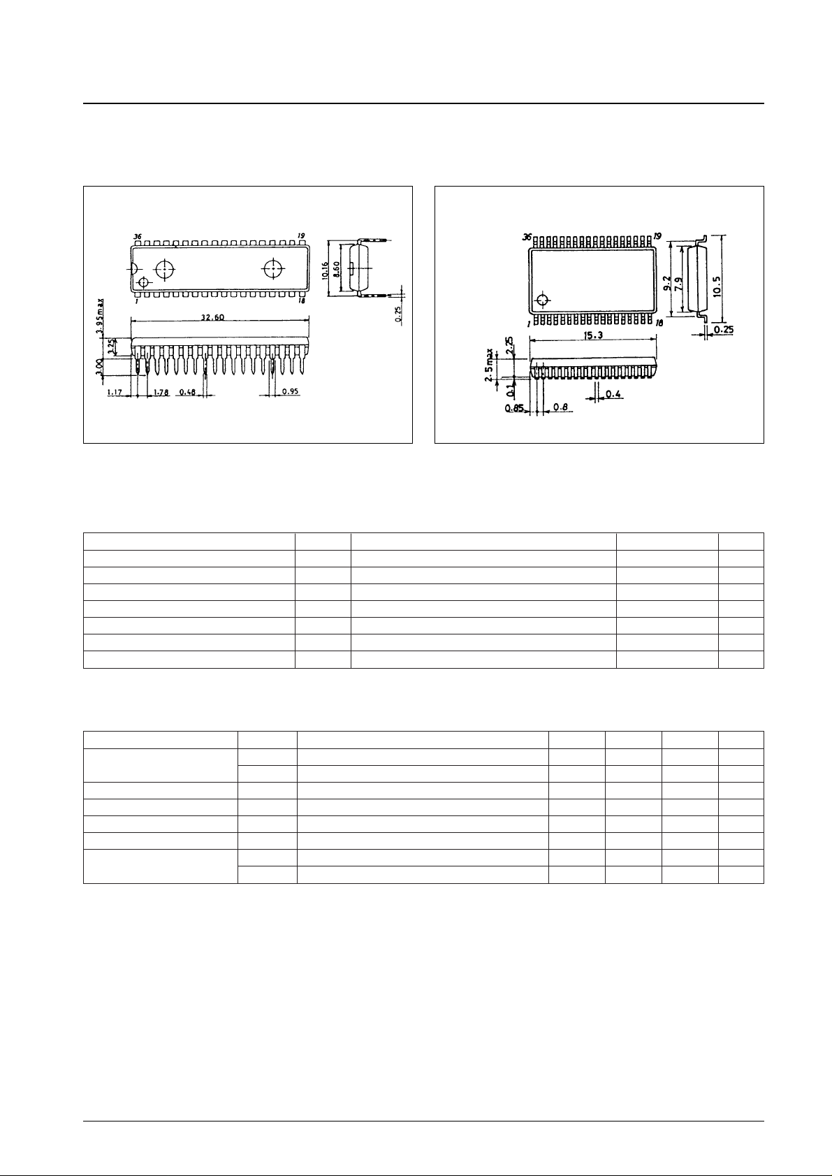
Package Dimensions
unit: mm unit: mm
3170-DIP36S 3129-MFP36SD
No. 5203-2/27
LC737212, 737212M
SANYO: DIP36S
[LC737212]
SANYO: MFP36SD
[LC737212M]
Specifications
Absolute Maximum Ratings at Ta = 25°C
Allowable Operating Ranges at Ta = 25°C
Parameter Symbol Conditions Ratings Unit
Maximum power supply voltage V
DD
max –0.3 to +6.5 V
Maximum input voltage V
IN
max –0.3 to VDD+0.3 V
Maximum output voltage V
OUT
max –0.3 to VDD+0.3 V
Allowable power dissipation Pd max Ta ≤ 70 ˚C 250 mW
Minimum load resistance P
L
min Between the DTMF and VSSpins 1 kΩ
Operating temperature Topr –30 to +70 °C
Storage temperature Tstg –40 to +125 °C
Parameter Symbol Conditions min typ max Unit
Supply voltage
V
DDP
Pulse mode 1.5 5.5 V
V
DDT
DTMF mode 2.0 5.5 V
Input high-level voltage V
IH
All input pins 0.7 V
DD
V
DD
V
Input low-level voltage V
IL
All input pins V
SS
0.3 V
DD
V
Key contact resistance R
KI
3.0 kΩ
Keypad capacitance C
KI
330 pF
Oscillator element rating
f Center frequency = 3.579545 MHz –1.3 +1.3 %
R
S
100 Ω
Page 3

Electrical Characteristics at Ta = 25°C, fosc = 3.579545 MHz
AC Characteristics at Ta = 25°C, fosc = 3.579545 MHz
No. 5203-3/27
LC737212, 737212M
Parameter Symbol Conditions min typ max Unit
Operating current drain
I
DDP
Pulse output mode, outputs open, VDD= 3.0 V 0.3 0.5 mA
I
DDT
DTMF output mode,outputs open, VDD= 3.0 V 0.5 1 mA
Static current drain I
DD(ST)
Standby mode, outputs open, VDD= 1.5 to 5.5 V 1 µA
Memory retention voltage V
DR
Between VDDand V
SS
1 V
Memory retention current I
DR
VDD= 1 V 0.5 µA
The SOUT-ENA, OFF-HOOK, DPR, P/T, BMR,
I
IH1
ON-HOOK-DIAL IN, HOLD-OFF IN, DISCON IN, 1 µA
Input pin current
SI/KEY, OFF/ON-HOOK, and STORE pins, VIH= V
DD
The SOUT-ENA, OFF-HOOK, DPR, P/T, BMR,
I
IL1
ON-HOOK-DIAL IN, HOLD-OFF IN, DISCON IN, –1 µA
SI/KEY, OFF/ON-HOOK, and STORE pins, VIL= V
SS
I
ILK1
All key pins, VDD= 1.5 V, V
ILK
= V
SS
–20 µA
I
ILK2
All key pins, VDD= 5.5 V, V
ILK
= V
SS
–300 µA
Key pin current
I
OLK1
All key pins, VDD= 1.5 V, V
OLK
= 0.4 V 200 µA
I
OLK2
All key pins, VDD= 5.5 V, V
OLK
= 0.4 V 0.7 mA
Output pin leakage current I
OFF
VO= VDD, VDD= 5.5 V, with the output off, the DP,
1 µA
MUTE1, MUTE2, and S-OUT pins.
V
OH1
The K-TONE, HOLD-OUT, HOOK-CTL,
V
DD
– 0.5 V
and SP-CTL pins, VDD= 1.5 V, IOH= –250 µA
V
OH2
The K-TONE, HOLD-OUT, HOOK-CTL,
V
DD
– 1 V
Output pin voltage
and SP-CTL pins, VDD= 5.5 V, IOH= –1 mA
V
OL1
The K-TONE, DP, MUTE1, MUTE2, SP-CTL,
0.4 V
HOLD-OUT, and HOOK-CTL pins, V
DD
= 1.5 V, IOL= 250 µA
V
OL2
The K-TONE, DP, MUTE1, MUTE2, SP-CTL,
0.4 V
HOLD-OUT, and HOOK-CTL pins, V
DD
= 5.5 V, IOL= 1 mA
Parameter Symbol Conditions min typ max Unit
Key debounce time T
KD
30 ms
Pin chatter exclusion time T
PCHT
OFF-HOOK, P/T, ON-HOOK-DIAL, IN HOLD OFF IN 45 ms
Key scan frequency f
KSC
258.9 HZ
Key tone frequency f
KT
1035.7 HZ
Key tone output time T
KT
30.9 ms
In Pulse mode at 10 pps 3.88 3.9 3.93 s
Auto-pause time T
AP
In Pulse mode at 20 pps 3.88 3.9 3.93 s
DTMF mode 3.88 3.9 3.93 s
DTMF output time T
MFON
98 100 102 ms
DTMF interdigit pause time T
MFOFF
93 95 97 ms
Hooking time T
HK
700 710 720 ms
Hooking pause time T
HKP
0.98 1.0 1.02 s
Memory store confirmation
f
KST
2071.4 Hz
tone frequency
Memory store confirmation
T
KSTON
278.1 ms
tone output time
Low tone amplitude V
OR
VDD= 3.5 V, RL= 10 kΩ 165 200 240 mVrms
Tone output ratio dBCR V
DD
= 2.0 to 5.5 V, RL= 10 kΩ 1 2 3 dB
Tone output distortion DIS V
DD
= 2.0 to 5.5 V, RL= 10 kΩ 10 %
Oscillator start time T
START
VDD= 1.5 to 5.5 V 30 ms
V
DD
= 3.0V 1 ms
Page 4

Pulse Dialing Output/fosc = 3.579545 MHz
DTMF Output/fosc = 3.579545 MHz
Pin Assignment
No. 5203-4/27
LC737212, 737212M
Dialing Interdigit Make
DPR pin BMR pin
pulse rate pause percent
V
SS
V
DD
9.94 pps 834.2 ms 33.2%
V
DD
V
DD
19.89 pps 525.2 ms 33.2%
V
SS
V
SS
9.94 pps 834.2 ms 39.2%
V
DD
V
SS
19.89 pps 525.2 ms 39.2%
Input
Output frequency [Hz]
Deviation [%]
Standard LC737212
R1 697 697.0 +0.01
R2 770 770.1 –0.02
R3 852 852.3 –0.03
R4 941 942.0 –0.11
C1 1209 1209.3 –0.03
C2 1336 1335.7 +0.03
C3 1477 1476.7 +0.02
C4 1633 1633.0 +0.00
Top view
Page 5
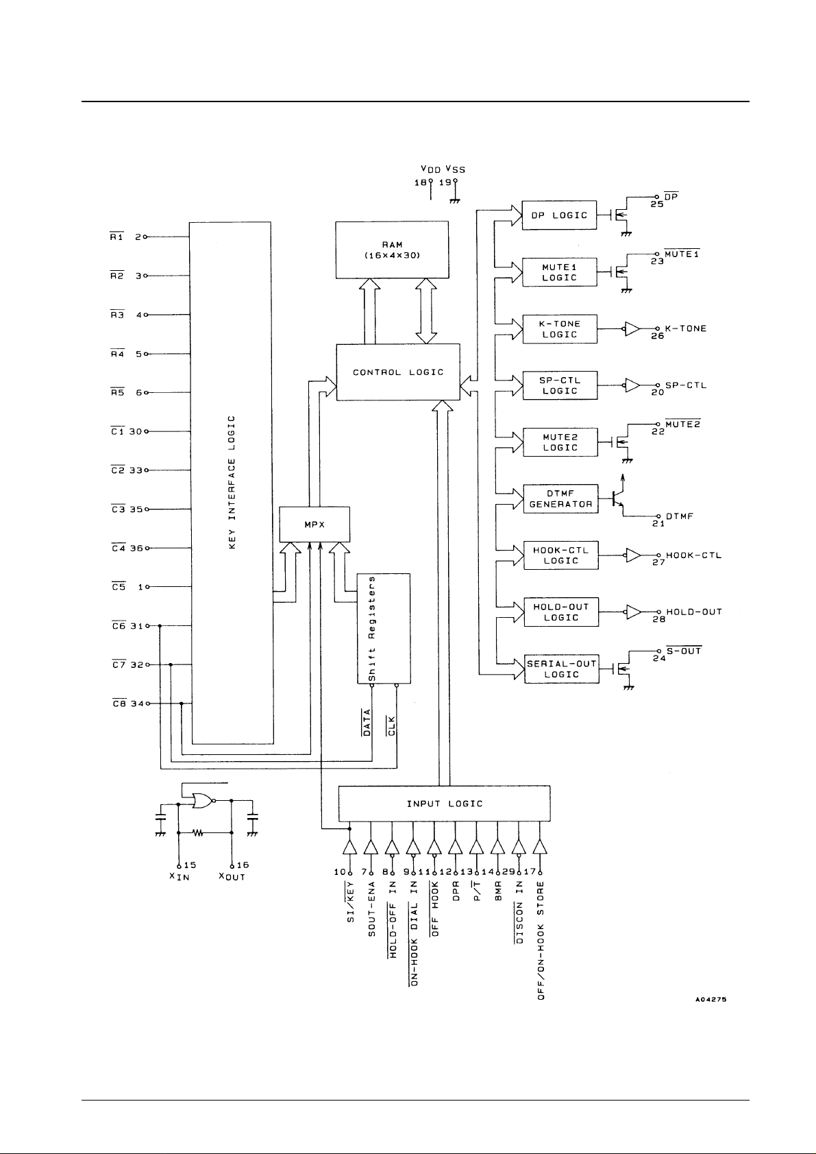
Block Diagram
No. 5203-5/27
LC737212, 737212M
Page 6

Keypad Layout
Key Matrix Functions (when the SOUT-ENA pin is high)
Digits 1 to 9, 0: Dialing data
* and #: DTMF dialing data
In pulse mode, the * key switches the LC737212/M to DTMF mode.
F: Flash (0.71 second)
M: Quick-dialing address specification (only in the on-hook state, sets up memory store mode)
R/P: Redial, pause (3.9 seconds), clear the paused state
HOLD ON/OFF: Controls the on/off state of hold mode
STORE: Sets up memory store mode.
A1 to A5: One-touch dialing key
00 to 17: Definable function keys
The keypad is formed as a matrix using the key input pins (R1 to R5 and C1 to C8) and supports 40 keys. A given key is
input by shorting or grounding the column pin and the row pin for that key. To prevent discharge of the backup battery
due to inadvertent key presses in standby mode (when the circuit is disconnected from the telephone line), key input by
shorting is not accepted. This means that if on-hook storing of telephone numbers in memory is selected, the application
must implement STORE key (or M key) input by grounding the ROW pin and COLUMN pin.
• Digit keys (1 to 9 and 0)
— Dialing data keys
— Quick-dialing memory address specification keys
• * and # keys
— DTMF mode: The * and # keys function as dial data keys
— Pulse mode: * ... Pulse/tone switching key
# ... Unused.
• F key (flash key)
Invokes an operation equivalent to 0.71-second hooking implemented by turning on the DP output for 0.71 second.
Although a 1-second pause is automatically inserted, the following dialing data may be entered during that period.
Redialing is possible after a flash operation.
• M key (memory key)
When on-hook memory registration is set up, the system switches from standby mode to memory registration mode
when the M key is pressed. The address of the dialing memory is specified by combination of the digit keys that are
pressed immediately after the M key. The system operates as follows when the memory address operation is performed
incorrectly.
No. 5203-6/27
LC737212, 737212M
1 2 3 F 00 05 10 15
4 5 6 M 01 06 11 16
7 8 9 R/P 02 07 12 17
* 0 #
HOLD
03 08 13 A4
ON/OFF
A1 A2 A3 STORE 04 09 14 A5
R1
to
R5
C1 to C8
Page 7

Memory readout
Memory store
• R/P key
After connecting to the line, the R/P functions as a redial key as long as the system has not performed a dialing output
operation. In manual dialing mode, the R/P key functions as the pause data key.
When dialing from memory:
— During a pause operation: Cancels the pause
— While dialing: Inserts a pause
During a redial operation:
— During a pause operation: Cancels the pause
— While dialing: Ignored
If two or more pause characters occur in the data, the pause cancel operation will cancel all pending pauses in a single
operation.
• STORE key
Pressing the STORE key sets the system to memory store mode. Pressing the STORE key again during a memory store
operation cancels all input data.
• HOLD ON/OFF key
Controls the on/off state of off-hook mode. No key tone is output at this time.
• Keys A1 to A5
These are the one-touch auto-dialing keys. Pressing one of these keys outputs the corresponding memory data from the
DP and DTMF pins.
• Keys 00 to 17
These are user-defined keys. When one of these keys is pressed, the LC737212/M outputs the corresponding status and
key code from the serial interface.
No. 5203-7/27
LC737212, 737212M
Page 8

No. 5203-8/27
LC737212, 737212M
Pin Functions
Pin No. Symbol Function
1 C5 Column input
2 R1
3 R2
4 R3 Row input
5 R4
6 R5
7 SOUT-ENA Serial output enable, H: enable, L: disable
8 HOLD-OFF IN Hold mode clear input; falling edge detection.
9 ON-HOOK DIAL IN On-hook dialing input; falling edge detection
10 SI/KEY Serial input/keypad input switching
11 ON-HOOK Hook-switching input
12 DPR Dialing pulse rate switching; H: 20 pps, L: 10 pps
13 R/T Pulse/tone switching; H:pulse, L: tone
14 BMR Make percentage switching input; H: 33%, L: 39%
15 XIN
Oscillator circuit. Connect either a crystal or ceramic oscillator element with a
16 XOUT
frequency of 3.58 MHz between these pins.
17 OFF/ON-HOOK STORE Off-hook store/on-hook store switching
18 V
DD
Power supply
19 V
SS
20 SP-CTL Speaker reception control output; complementary output
21 DTMF DTMF output; npn emitter-follower output
22 MUTE2 DTMF mute output; n-channel open drain output
23 MUTE1 DP and K-TONE muting output; n-channel open drain output
24 S-OUT Serial data output; n-channel open drain output
25 DP Dialing pulse output; n-channel open drain output
26 K-TONE K-tone output; complementary output
27 HOOK-CTL Hook control output; complementary output
28 HOLD-OUT Hold mode output; complementary output
29 DISCON IN Disconnect input
30 C1
31 C6
32 C7
33 C2 Column inputs
34 C8
35 C3
36 C4
Page 9

• SOUT-ENA
Normaly set high. Serial output and Dial output are enabled when this pin is set high.
• HOLD OFF IN
Hold mode is cleared when a falling edge is detected on this pin. HOLD-OFF pin inputs are not accepted for the 0.5
seconds immediately following a transition to on-hook hold mode.
• ON-HOOK-DIAL IN
This pin toggles an on/off state on each input falling edge. When the telephone is on hook, this pin toggles the on/off
state of on-hook dialing mode. When the telephone is off hook, this pin toggles the on/off state of monitor mode.
• SI/KEY
The keypad is set to input mode when this pin is set low. When this pin is set high, serial input is enabled. In this state,
all keypad inputs are pulled up by built-in resistors, and the pins C6 to C8 function as the serial interface input pins.
C6 = serial clock input
C7 = serial data input
C8 = strobe input
• OFF-HOOK
This pin is the hook state switching input.
• DPR
This pin is the dialing pulse rate switching input. (H: 20 pps, L: 10 pps)
• P/T
This pin is the dialing signal switching input. (H: pulse, L: DTMF) This pin can only switch from pulse to DTMF. This
allows mixed-mode dialing, i.e. switching modes during dialing.
• DISCON IN
Setting this pin low switches the LC737212/M to low power mode and forcibly stops the oscillator circuit. All outputs
are turned off in low power mode. (The n-channel open-drain outputs go to the high-impedance state, and the
complementary outputs go low.) The internal states of the LC737212/M are reset when this pin goes high.
We recommend setting the DISCON pin low when power is first applied, and setting it high after the power-supply
voltage (VDD) has reached or exceeded 1.5 volts.
• BMR
This pin sets the break/make ratio for the dialing pulse output. (H: 33.2%, L: 39.2%)
• OFF/ON-HOOK STORE
This pin switches the memory storing mode.
H: Off-hook store (Memory stored with the telephone line connected.)
L: On-hook store (Memory stored with the telephone line disconnected.)
No. 5203-9/27
LC737212, 737212M
Off-hook input On-hook Dial input Status
H H STANDBY
H L ON-HOOK DIAL
L H OFF-HOOK DIAL
L L MONITOR
1 to 10 kΩ
0.1 to 10 µF
Page 10

• SP-CTL
This pin provides the speaker reception control output. This output is set on during the on-hook dialing, monitor, and
hold states. This is a complementary output.
• DTMF
The DTMF output pin. This is an npn emitter-follower output.
• MUTE2
The DTMF muting output. This output is turned on in synchronization with the DTMF output. This is an n-channel
open-drain output. The wired OR with the MUTE1 output can be taken.
• MUTE1
The DP and K-TONE muting output. This output is turned on in synchronization with the dialing pulse and K-TONE
outputs. This is an n-channel open-drain output. The wired OR with the MUTE2 output can be taken.
• S-OUT
The serial data output. This pin is used to output the internal status of the LC737212/M and the keypad data. This is an
n-channel open-drain output.
• DP
The dialing pulse output. This is an n-channel open-drain output.
• K-TONE
This pin outputs the key input confirmation tone (1036 Hz, 31 ms) and the memory store confirmation tone (2073 Hz,
279 ms). This is a complementary output.
• HOOK-CTL
The circuit control output. A high level is output when the circuit is connected. This is a complementary output.
• HOLD-OUT
The hold control output. A high level is output during a hold. This is a complementary output.
• XIN and XOUT
The oscillator connection pins. Connect a 3.579545-MHz oscillator element. No other external components are
required if a crystal oscillator element with built-in feedback resistor and capacitor components is used. Two 30-pF
capacitors are required if a ceramic resonator is used.
• R1 to R5 and C1 to C8
The keypad connections.
• VDDand V
SS
The power supply connections.
No. 5203-10/27
LC737212, 737212M
Page 11

No. 5203-11/27
LC737212, 737212M
Pin Internal Circuit
Pin No. Pin Internal equivalent circuit
1 to 6
30 to 36
R1 to R5
C1 to C8
7 to 14
17
29
SOUT-ENA
HOLDOFF IN
ON-HOOKDIAL IN
SI/KEY
OFF-HOOK
DPR
P/T
BMR
OF/ON-HOOK STORE
DISCON IN
15
X
IN
16
X
OUT
22 to 25
MUTE2
MUTE1
S-OUT
DP
20
26 to 28
SP-CTL
K-TINE
HOOK-CTL
HOLD-OUT
21 DTMF
Page 12

Key Operations
↓: On hook ↑: Off hook
: Key input
Dn: Pulse output Dn: Tone output
Timing Charts
Pulse dialing
Item Key Input Dialing Output
↑
,
• • • • •
Dn
D
2
D
1
↑
,
• • • • •
Dn
D
2
D
1
Normal dialing and redialing (pulse mode)
Normal dialing using the key (pulse mode)
No. 5203-12/27
Dn
R/P
Normal dialing (pulse mode)
Normal dialing including mode changes
(pulse mode at the start of the operation)
Memory store and
readout
Quick dialing
One-touch dialing
Normal
Redialing
Using keys
Using the P/T
switch
Store (pulse mode)
Readout
Store (tone mode)
Readout
D
1
, D
2
• • • • • Dn
D
1
, D
2
D3
D
1
, D
2
• • • • • Dn
D
1
, D
2
• • • • • Dn
D1, , D2, D
3
D1, D2, D
3
D1, D2, D
3
3.9 s
3.9 s
. . .
. .
D
1
, , D2, D
3
3.9 s
. .
↑
, , ,
D
3
R/P
D
2
D
1
↓
↑
R/P
↑
, , ,
D
3
D
2
*
D
1
↑
,
(P/T↓),
,
D
3
D
2
D
1
↓
D
5
D
4
M
D
3
D
2
D
1
STO
↑
D
5
D
4
M
↓
A
1
D
3
D
2
D
1
STO
↑
A1
LC737212, 737212M
.
Page 13

DTMF dialing
Flash operation
Pulse/tone mixed dialing
After the pulse dialing (including IDP) has completed, when DTMF key input operations are performed, DTMF signals are output continuously while keys are
pressed.
No. 5203-13/27
LC737212, 737212M
Page 14

Pulse/Tone Mixed Dialing (using automatic pausing)
If a DTMF key operation is performed during dialing pulse output (including IDP), the K-TONE signal will be output continuously while keys are pressed.
Then, after the pulse dialing completes, the LC737212/M will pause for 3.9 seconds and then output the DTMF signals.
No. 5203-14/27
LC737212, 737212M
Page 15

LC737212 and LC737212M Operating Specifications
1. IC Internal Status
The LC737212 and LC737212M have 14 internal states. Table 1 presents a functional overview of these states. The
individual status bits have the following interpretations.
D4: SP-CTL output
D3: HOOK-SW information
D2: Memory store
D1: Hold (the HOLDOUT output)
D0: Dialing allowed.
However, note that during standby key acquisition, D1 and D2 do not have the above meanings.
Table.1 State Table
2. Dialing Output Specifications
Dialing output is possible in the off-hook dialing, on-hook dialing, and monitor modes.
The output pulse make percentage in pulse mode can be specified to be 33.2 or 39.3% with the BMR pin.
The output pulse rate in pulse mode can be set to be 10 or 20 pps with the DPR pin.
The LC737212 can generate 12 DTMF dialing signals in DTMF mode. (If serial input is used, it can generate 16
DTMF dialing signals.)
DTMF signals are output continuously as long as the corresponding key is held down.
The LC737212 guarantees a minimum DTMF output time of about 100 ms, and also guarantees a minimum IDP of
about 100 ms.
If the mode is changed (with the P/T pin or * key) during a pulse dialing operation and then DTMF data is keyed in,
the system automatically inserts a 3.9 second pause after completing the pulse dialing sequence and then outputs the
DTMF signals.
No. 5203-15/27
LC737212, 737212M
No. State HOOK-SW Function
HOOK- SP- HOLD- Dialing Status bits
Notes
CTL CTL OUT output D4 to D0
1 Standby ON Key input by shorting key pins disabled. OFF OFF OFF Disabled 01000
2
Standby with
ON
Keypad input enabled. Only the keypad
OFF OFF OFF Disabled 01110
Switched to from
key acquisition data is output through the serial interface. standby mode.
3 Off-hook dialing OFF Off-hook dialing mode ON OFF OFF Disabled 00001
4
Off-hook dialing with
OFF
Only the keypad data is output through the serial
ON OFF OFF Disabled 00000
Switched to from off-
key acquisition interface. Data is not written to the redial memory. hook dialing mode.
5 On-hook dialing ON On-hook dialing mode ON ON OFF Enabled 11001
6
On-hook dialing with
ON
Only the keypad data is output through the serial
ON ON OFF Disabled 11000
Switched to from off-
key acquisition interface. Data is not written to the redial memory. hook dialing mode.
7 Monitor OFF Monitor mode ON ON OFF Enabled 10001
8
Monitor with
OFF
Only the keypad data is output through the serial
ON ON OFF Disabled 10000
Switched to from
key acquisition interface. Data is not written to the redial memory. monitor mode.
9 Off-hook hold OFF Hold mode ON ON ON Disabled 10010
Switched to from offhook dialing mode.
10 On-hook hold ON Hold mode ON ON ON Disabled 11010
Switched to from onhook hold mode.
11 On-hook store ON Memory store more (circuit disconnected) OFF OFF OFF Disabled 01100
Switched to from
standby mode.
12 Off-hook store OFF Memory store more (circuit connected) ON ON OFF Disabled 00100
Switched to from offhook dialing mode.
13 Off-hook dialing and store ON Memory store more (circuit connected) ON ON OFF Disabled 11100
Switched to from offhook dialing mode.
14 Monitor store OFF Memory store more (circuit connected) ON ON OFF Disabled 10100
Switched to from
monitor mode.
Page 16

If the mode is changed after a pulse dialing operation and DTMF data is keyed in, the system does not automatically
insert a pause, but rather outputs the DTMF data as it is keyed in.
The pause key (the R/P key used as the second or later digit) can be used to enter pause data.
If pause data and mode change data (MC) are entered consecutively, the system pauses for 3.9 seconds.
After connecting to the line, the first time the R/P key is pressed, the system will redial the previously entered dialing
data.
3. Memory Output Specifications
The LC737212/M provides five 16-digit memory locations for one touch dialing memory, 20 16-digit memory
locations for quick-dialing memory, a 16-digit buffer memory for store operations, and a 63-digit redialing memory.
A single digit of memory can hold a single dialing data item (1 to 9, 0, *, or #), a single mode change data item
(MC), or a single pause data item (P).
• RD memory
The LC737212/M includes a 63-digit buffer memory that also functions as the redial memory, and thus is called the
RD memory. The keyed in input data is stored sequentially in the RD memory.
— Dialing data stored in RD memory is read out at the specified dialing rate and output from the DP or DTMF pin.
— Dialing numbers that exceed 63 digits is possible. The system writes the key data that exceeds 63 digits starting at
the beginning (location 0) of RD memory and outputs that data.
— However, this means that redialing numbers that exceed 63 digits is not possible since the dialing data is not all
correctly retained in RD memory.
• Dialing memory (one-touch dialing and quick dialing)
— LC737212 provides five locations (A1 to A5) for one-touch dialing, and 20 locations (M00 to M19) for quick
dialing.
— Each of these dialing memory locations holds 16 digits of dialing data plus the output format (pulse or DTMF) for
the start of the data.
— When a dialing memory location is accessed, its content is copied to RD memory and then the LC737212/M dials
that number by reading it out of RD memory.
— If a number stored as DTMF in dialing memory is read out after a pulse dialing operation, a mode change (MC)
data item is automatically inserted in RD memory.
— After a DTMF signal is output, if data registered as pulse data is read out from a dialing memory, that data will be
output as DTMF signals.
• Data store buffer memory
— This memory is used when storing a number in dialing memory.
4. Off-Hook Hold and On-Hook Hold Modes
Pressing the HOLD key switches between off-hook dialing mode and hold (off-hook hold mode).
In hold mode, the HOLD-OUT and SP-CTL outputs are turned on.
Dialing is disabled in hold mode.
It is not possible to hold during dialing.
Placing the phone on hook switches the system from off-hook hold mode to on-hook hold mode.
Lifting the receiver switches the system from on-hook hold mode to off-hook hold mode.
Hold is cleared by a falling edge on the HOLD-OFF IN pin.
— This switches from off-hook hold mode to on-hook dialing mode.
— This also switches from on-hook hold mode to standby mode.
After switching to off-hook hold mode, falling edges on the HOLD-OFF IN pin are not detected for 0.5 second.
5. On-Hook Dialing
Falling edges on the ON-HOOK DIAL IN input switches the system between standby mode and on-hook dialing
mode.
In on-hook dialing mode, the HOOK-CTL and SP-CTL pins output high levels.
It is not possible to hold when the system is in on-hook dialing mode.
Lifting the receiver switches the system to off-hook dialing mode.
No. 5203-16/27
LC737212, 737212M
Page 17

6. Monitor Mode
Falling edges on the ON-HOOK DIAL IN input switches the system between off-hook dialing mode and monitor
mode.
In monitor mode, the HOOK-CTL and SP-CTL pins output high levels.
It is not possible to hold when the system is in monitor mode.• Placing the receiver on-hook switches the system
to on-hook dialing mode.
7. Memory Store Function
On-hook (with the line disconnected) and off-hook (with the line connected, including on-hook dialing and monitor
modes) storing can be selected. The On/OFF-HOOK store pin is used for this selection.
Data is stored in memory in store mode. The following key sequences switch the system to store mode.
— On-hook (disconnected from the line) ... Pressing either the STORE or M key
— Off-hook (connected to the line) ... Pressing the STORE key
Data is written to a memory store buffer memory (16 digits) by keying in that dialing data. Key confirmation tones
(1036 Hz, 31 ms) are output from the K-TONE pin during this operation. Keyed data corresponding to a seventeenth
or later digit is ignored and the confirmation tone is not output for those digits.
Specifying the memory address copies the contents of the memory store buffer memory to the specified address and
completes the memory store operation. A memory store confirmation tone (2072 Hz, 279 ms) is output from the KTONE pin at this point.
The data at a given address can be deleted by switching to store mode and then specifying the address without
entering any dialing data.
8. Key Acquisition Modes
In these modes, the LC737212/M simply accepts key input and transmits the corresponding key code and status over
the serial interface. Data from the keypad is not written to the RD memory and dialing is not performed.
• Standby key acquisition mode
— Pressing the 00 key when the SI/KEY pin is low, or entering a code value of 20 when the SI/KEY pin is high,
switches the LC737212/M between standby mode and standby key acquisition mode.
— If, and only if, on-hook memory storing is selected, pressing the STORE key will switch the system to on-hook
store mode.
• Off-hook key acquisition mode, on-hook dialing key acquisition mode, and monitor key acquisition mode
— In modes that allow dial output, entering a code value of 20 over the serial interface will switch the LC737212/M
to the corresponding key acquisition mode.
— Even if the LC737212/M is in a key acquisition mode, dialing data entered over the serial interface will be dialed.
9. Serial Output
During key input and when the system's internal mode change, the LC737212/M outputs the corresponding status
data from the S-OUT pin. Values of 0 and 1 are expressed by the length of the period the n-channel open-drain
output pin is in the on state, and data is grouped in 4-bit units for output.
0 = 280 µs, 1 = 760 µs, inter-bit interval = 560 µs
Interval between 4-bit groups = 1440 µs
(In memory content readout mode only, the 4-bit group interval is 1520 µs.)
• During Key Input
— This data consists of 16 bits, starting with a bit (always 0) that indicates that this data is key input data. The next 2
bits are dialing related data, then the next 5 bits indicated the LC737212/M internal status, and finally, the last 8
bits indicate the key data.
— The data for all key presses that were longer than 30 ms (the key bounce (chatter) exclusion time) are output. (For
example, data key presses when the system is in hold mode are not dialed, but are output from S-OUT as key data.)
No. 5203-17/27
LC737212, 737212M
Page 18

* Timing chart · Assuming the key was pressed in normal mode.
3
No. 5203-18/27
LC737212, 737212M
D15
D14
D13
D12
Indicates that this is for key input. Always 0
Indicates the key data write type. Pulse = 1, DTMF = 0
Indicates dialing output. Output in progress = 1, output done = 0.
Upper bit of the IC internal status
D11
D10
D9
D8
Lower four bits of the IC internal status.
D7
D6
D5
D4
Key code KCU
D3
D2
D1
D0
Key code KCL
Page 19

Key Codes
No. 5203-19/27
LC737212, 737212M
KEY KEY CODE
KEY ROW COL D7 D6 D5 D4 D3 D2 D1 D0 HEX
1 1 1 1 0 0 0 0 0 0 1 8 1
2 1 2 1 0 0 0 0 0 1 0 8 2
3 1 3 1 0 0 0 0 0 1 1 8 3
4 2 1 1 0 0 0 0 1 0 0 8 4
5 2 2 1 0 0 0 0 1 0 1 8 5
6 2 3 1 0 0 0 0 1 1 0 8 6
7 3 1 1 0 0 0 0 1 1 1 8 7
8 3 2 1 0 0 0 1 0 0 0 8 8
9 3 3 1 0 0 0 1 0 0 1 8 9
0 4 2 1 0 0 0 1 0 1 0 8 A
*/T 4 1 1 0 0 1 1 0 1 1 9 B
# 4 3 1 0 0 1 1 1 0 0 9 C
F 1 4 0 1 0 0 0 0 1 1 4 3
M 2 4 0 1 0 0 0 1 0 1 4 5
HOLD 4 4 0 1 0 0 0 1 1 1 4 7
STORE 5 4 0 1 0 0 1 0 0 1 4 9
R/P 3 4 0 1 1 0 1 0 0 1 6 9
Page 20

Key Codes
• Mode change (when the IC internal state changes)
— Here the data consists of eight bits, one bit (which is always 1) used to differentiate this data from key data, and
seven bits expressing the mode change. This data is output when the internal state changes, the P/T pin changes, or
when dialing completes.
— D5 expresses the state of the P/T pin.
1 = pules, 0 = DTMF
In the following cases, the status is not output even if the P/T pin changes state.
In standby mode, off-hook hold mode, or on-hook hold mode.
After tone data (including MC) is written to RD memory.
— When a memory location that does not have data stored is accessed:
If not dialing: the status when dialing completed is output as serial data.
If dialing: A serial output operation is not performed.
— If a redial operation is attempted when redial is disabled (when the last number dialed exceeded 63 digits) the
status when dialing completed is output as serial data.
* Timing Chart
· From the standby state to off hook, and then to off-hook dialing
· With the P/T switch set to P
No. 5203-20/27
LC737212, 737212M
KEY KEY CODE
KEY ROW COL D7 D6 D5 D4 D3 D2 D1 D0 HEX
00 1 5 0 0 0 0 0 0 0 0 0 0
01 2 5 0 0 0 0 0 0 0 1 0 1
02 3 5 0 0 0 0 0 0 1 0 0 2
03 4 5 0 0 0 0 0 0 1 1 0 3
04 5 5 0 0 0 0 0 1 0 0 0 4
05 1 6 0 0 0 0 0 1 0 1 0 5
06 2 6 0 0 0 0 0 1 1 0 0 6
07 3 6 0 0 0 0 0 1 1 1 0 7
08 4 6 0 0 0 0 1 0 0 0 0 8
09 5 6 0 0 0 0 1 0 0 1 0 9
10 1 7 0 0 0 1 0 0 0 0 1 0
11 2 7 0 0 0 1 0 0 0 1 1 1
12 3 7 0 0 0 1 1 0 1 0 1 2
13 4 7 0 0 0 1 0 0 1 1 1 3
14 5 7 0 0 0 1 0 1 0 0 1 4
15 1 8 0 0 0 1 0 1 0 1 1 5
16 2 8 0 0 0 1 0 1 1 0 1 6
17 3 8 0 0 0 1 0 1 1 1 1 7
A1 5 1 0 0 1 1 0 0 0 1 3 1
A2 5 2 0 0 1 1 0 0 1 0 3 2
A3 5 3 0 0 1 1 0 0 1 1 3 3
A4 4 8 0 0 1 1 0 1 0 0 3 4
A5 5 8 0 0 1 1 0 1 0 1 3 5
state
Page 21

10. Serial Input
The following control can be performed using serial input.
Keypad input replacement (except for user-defined keys)
Setting the status bits (e.g., setting the on-hook dialing mode on/off)
Reading out the content of dialing memory
Setting the output port on/off states (including the DTMF signal output)
• Serial input format
— Set the SI/KEY input pin high. This causes all the keypad inputs to be pulled up and the C6 to C8 pins function as
serial input pins for an internal shift register.
C6 = Clock input
C7 = Data input
C8 = Strobe input
— Data is written on the falling edge of the clock input
— The period when the strobe input is low is equivalent to the period when a keypad key is pressed.
— The data consists of 8 bits.
— Codes other than the 40 codes defined as keypad keys are defined as input data codes in the serial input.
— This allows controls other than the DPR and BMR controls to be input serially.
No. 5203-21/27
LC737212, 737212M
D7
D6
D5
D4
D3
D2
D1 D0
D0
Page 22

Serial Input Code Table
No. 5203-22/27
LC737212, 737212M
Serial code
Command Function or operation
(HEX)
00
01
02
03
04 Serial readout of quick-dialing memory locations 00 to 09
05
06
07
08
09
0A
0B
0C Serial readout of one-touch memory locations A1 to A5
0D
0E
0F Serial readout of the buffer memory used for storing to memory
10
11
12
13
14 Serial readout of quick-dialing memory locations 10 to 19
15
16
17
18
19
1A
Undefined
1B
1C
1D Serial readout of redial memory
1E 1C: digits 1 to 16 1D: Digits 17 to 32
1F 1E: digits 33 to 48 1F digits 49 to 63
20 Key acquisition mode on/off setting
21 to 2F Undefined
30 The same function as the A1 one-touch dialing key.
31 A1
32 A2
33 A3 The same functions as the one-touch dialing keys A1 to A5
34 A4
35 A5
36 to 3E The same function as the A1 one-touch dialing key
3F Cancels a memory store operation if one is in progress. Otherwise identical to the A1 key.
40 to 42 Undefined
43 F Identical to the F1 key.
44 RD Cancels redial or pause operations.
45 M Identical to the M key.
46 CLR Clears all memories. This function is enabled in memory store mode.
47 HOLD Identical to the HOLD key.
48 Undefined
49 STORE Identical to the STORE key.
4A OHD-ON On-hook dial and monitor mode setting (OHD-ON)
4B to 4C Undefined
4D RDINH Disables redial.
Continued on next page.
Page 23

No. 5203-23/27
LC737212, 737212M
Continued from preceding page.
Serial Code
Command Function or operation
(HEX)
4E DTMF output off
4F DISCON Initial settings (DISCON)
50 to 5F Undefined
60 to 6F R/P Identical to the R/P key.
70 to 7F Undefined
80 Undefined
81 1
82 2
83 3
84 4 Identical to the dial data keys 1 to 8.
85 5
86 6
87 7
88 8
89 9
Identical to the dial data keys 9 and 0.
8A 0
8B, 8C Illegal value
8D Pause data
8E Undefined
8F Illegal value
90 Undefined
91 to 9A Illegal in pulse mode. Dialing data when the IC is in tone mode.
9B * Identical to the dial data key “*”.
9C # Identical to the dial data key “#”.
9D Illegal in pulse mode. Pause data when the IC is in tone mode.
9E Undefined
9F Illegal value
A0, A1 Undefined
A2 MC Converts input data from pulse to DTMF. Illegal in tone mode.
A3 to AF P1/DFIN Undefined
B0 to BF P2 Undefined
C0 to CF Undefined
D0 Outputs the DTMF signal for 1
D1 Outputs the DTMF signal for 4
D2 Outputs the DTMF signal for 7
D3 Outputs the DTMF signal for *
D4 Outputs the DTMF signal for 2
D5 Outputs the DTMF signal for 5
D6 Outputs the DTMF signal for 8
D7 Outputs the DTMF signal for 0
D8 Outputs the DTMF signal for 3
D9 LCHN Left channel N output
DA LV
SS
Left channel ground. Normally 0 V.
DB Outputs the DTMF signal for #
DC Outputs the DTMF signal for A
DD Outputs the DTMF signal for B
DE Outputs the DTMF signal for C
DF Outputs the DTMF signal for D
E0 Sets the S-OUT output off
E1 Sets the S-OUT output on
E2 Sets the HOLD output off
E3 Sets the HOLD output on
E4 Sets the HK-CTL output off
Continued on next page.
Page 24

Continued from preceding page.
Note: The undefined command codes are ignored.
• Functions unique to the serial input commands
— When the SI/KEY pin is high, inputting code values 00 to 19 or 1C to 1F serially causes the contents of the
corresponding dialing memory to be output from the S-OUT pin.
— All data is grouped into four-bit groups and output. After first outputting the output format (pulse = 1111, DTMF =
1110), the LC737212/M outputs the dial data. The data value 0000 indicates that output has completed.
— See item (9) concerning serial output on page 17 for details on the output format for the data from the S-OUT pin.
— RD memory data (63 digits) is read out 16 digits at a time in four operations.
— When redial memory is disabled, attempts to read out RD memory (1C) serially will result in the output of either
F0 or E0.
Data in dialing memory is represented as shown in the table.
Switching Output Ports On and Off
— When the SI/KEY pin is high, inputting the following code values serially sets the corresponding output port on or
off. Since these commands directly write to the output port data latch, they do not change the internal status,
memory or other aspects.
S-OUT ON (E1) OFF (E0)
HOLD ON (E3) OFF (E2)
HK-CTL ON (E5) OFF (E4)
K-TONE 1 kHz (E7) 2 kHz (E6)
SP-CTL ON (E9) OFF (E8)
MUTE2 ON (EB) OFF (EA)
MUTE1 ON (ED) OFF (EC)
DP ON (EF) OFF (EE)
No. 5203-24/27
LC737212, 737212M
Serial code
Command Function or operation
(HEX)
E5 Sets the HK-CTL output on
E6 Turns on the K-TONE 2-kHz frequency for 279 ms
E7 Turns on the K-TONE 1-kHz frequency for 31 ms
E8 Sets the SP-CTL output off
E9 Sets the SP-CTL output on
EA Sets the MUTE2 output off
EB Sets the MUTE2 output on
EC Sets the MUTE1 output off
ED Sets the MUTE1 output on
EE Sets the DP output off
EF Sets the DP output on
F0 to FF SREQ Reads out the status data serially (SREQ)
Dialing Data
Representation
Dialing Data
Representation
in RAM in RAM
1 0001 9 1001
2 0010 0 1010
3 0011 * 1011
4 0100 # 1100
5 0101 Pause 1101
6 0110 MC (P → C) 1110
7 0111 Data end 000
8 1000
Page 25

When the K-TONE output is turned on, the MUTE1 output will operate in synchronization with the K-TONE
output.
When the HK-CTL output is turned on, key inputs due to shorting row pins and column pins will be accepted.
— When the SI/KEY pin is high, inputting the following code values serially can turn DTMF output on or off.
DTMF output ON 4 (D1) 1 (D0)
* (D3) 7 (D2)
5 (D5) 5 (D4)
0 (D7) 8 (D6)
6 (D9) 3 (D8)
# (DB) 9 (DA)
B (DD) A (DC)
D (DF) C (DE)
DTMF output OFF (4E)
Other Serial Input Codes
— SREQ (F0 to FF)
These commands output the IC's internal status from the SOUT pin. All the status items are valid.
— 20
Turns key acquisition mode on or off.
— 46 (CLR)
Inputting the CLR code in memory store mode erases all stored dialing data.
— 4A (OHD-ON)
Inputting the OHD-ON code in standby mode switches the system to on-hook dialing mode. Input the DISCON
code (4F) to return to standby mode.
— 8D (pause)
This command corresponds to 3.9-second pause data.
— A2 (MC)
Changes the dialing data input mode plug from pulse to tone. This is represented as 1110 in memory.
This is ignored and not written to memory if the dialing data input mode is tone mode.
Note that codes marked as undefined in the serial code table are ignored.
• Notes on serial input usage
— If the SI/KEY pin is switched from low to high and then to low again while a key is pressed, the LC737212/M will
receive two key presses for that key.
— TCLKD (The first SCLK input after the SI/KEY pin goes from low to high)
The LC737212/M monitors the SOUT output after SI/KEY goes high, and if there is no serial output due to a key
press after 3.5 ms or longer has elapsed, then it enables SCLK input. For all other cases, 35 ms or longer is
required.
— The IC will reliably output the status data from the SOUT pin if a status request command (FF) or a code 20
command in a mode other than hold or memory store mode is input. If this output does not appear for over 25 ms
(in cases other than serial readout from memory), the IC itself may have caused some sort of error. In such cases,
the IC must be re-initialized using the DISCON pin.
— We recommend always re-initializing the IC with the DISCON pin when receiving standby status. (At this time,
the IC will once again output the standby status data.)
No. 5203-25/27
LC737212, 737212M
Page 26

Status Diagram
Basic functions
Key acquisition mode
No. 5203-26/27
LC737212, 737212M
Page 27

PS No. 5203-27/27
LC737212, 737212M
This catalog provides information as of February, 1998. Specifications and information herein are subject to
change without notice.
■ No products described or contained herein are intended for use in surgical implants, life-support systems, aerospace
equipment, nuclear power control systems, vehicles, disaster/crime-prevention equipment and the like, the failure of
which may directly or indirectly cause injury, death or property loss.
■ Anyone purchasing any products described or contained herein for an above-mentioned use shall:
① Accept full responsibility and indemnify and defend SANYO ELECTRIC CO., LTD., its affiliates, subsidiaries and
distributors and all their officers and employees, jointly and severally, against any and all claims and litigation and all
damages, cost and expenses associated with such use:
➁ Not impose any responsibility for any fault or negligence which may be cited in any such claim or litigation on
SANYO ELECTRIC CO., LTD., its affiliates, subsidiaries and distributors or any of their officers and employees
jointly or severally.
■ Information (including circuit diagrams and circuit parameters) herein is for example only; it is not guaranteed for
volume production. SANYO believes information herein is accurate and reliable, but no guarantees are made or implied
regarding its use or any infringements of intellectual property rights or other rights of third parties.
During Store Operations
Off/On-HOOK STORE = 0
Off/On-HOOK STORE = 1
 Loading...