

Page 1
CMOS LSI
No. 5561
Overview
The LC73701M is a DTMP/pulse output dual-system
dialer CMOS LSI for use in push-button telephones. It
provides an on-chip serial interface and operates under the
control of data sent over that serial interface. The
LC73701M can be easily controlled by the system CPU
using this dedicated interface.
Functions
• Functions as a dialer that is controlled over a serial
interface.
• The built-in oscillator circuit (f
either a crystal oscillator or a ceramic resonator as its
oscillator element.
• The adoption of a high-precision (±0.04%) DTMF
signal frequency divider circuit allows a ceramic
resonator to be used as the oscillator element.
• The buffer memory can store up to 32 digits of 5-bit
data.
• Mode change and pause commands can also be stored as
data in the buffer memory.
• Pauses can be inserted automatically on mode changes
(auto-pause).
• A pause can be cancelled during that pause.
• The mode change function supports changing from pulse
to tone (single direction).
• Generates all 16 DTMF signals.
• The pulse dialer output can be turned on or off
arbitrarily.
• The pulse dialer output circuit can be selected to be
either an n-channel open drain or a complementary
circuit.
• The pulse dialer muting function can be turned on or off
arbitrarily.
• A redial function is provided.
• Flash operation is supported. (Data can be received
during flash operation.)
• The flash time can be switched to be either 277 or 707
ms.
• The pause time can be switched to be either 2 or 4
seconds.
• Hooking pause operation is supported. (1.2 s or 801 ms)
• The dial pulse rate can be specified to be either 10 pps
or 20 pps.
= 4.19 MHz) can use
OSC
LC73701M
Serial Interface Dialler
• The dial pulse make ratio can be specified to be either
33 or 39%.
• Wide operating voltage range
Pulse mode: VDD= 1.5 to 5.5 V
DTMF mode: V
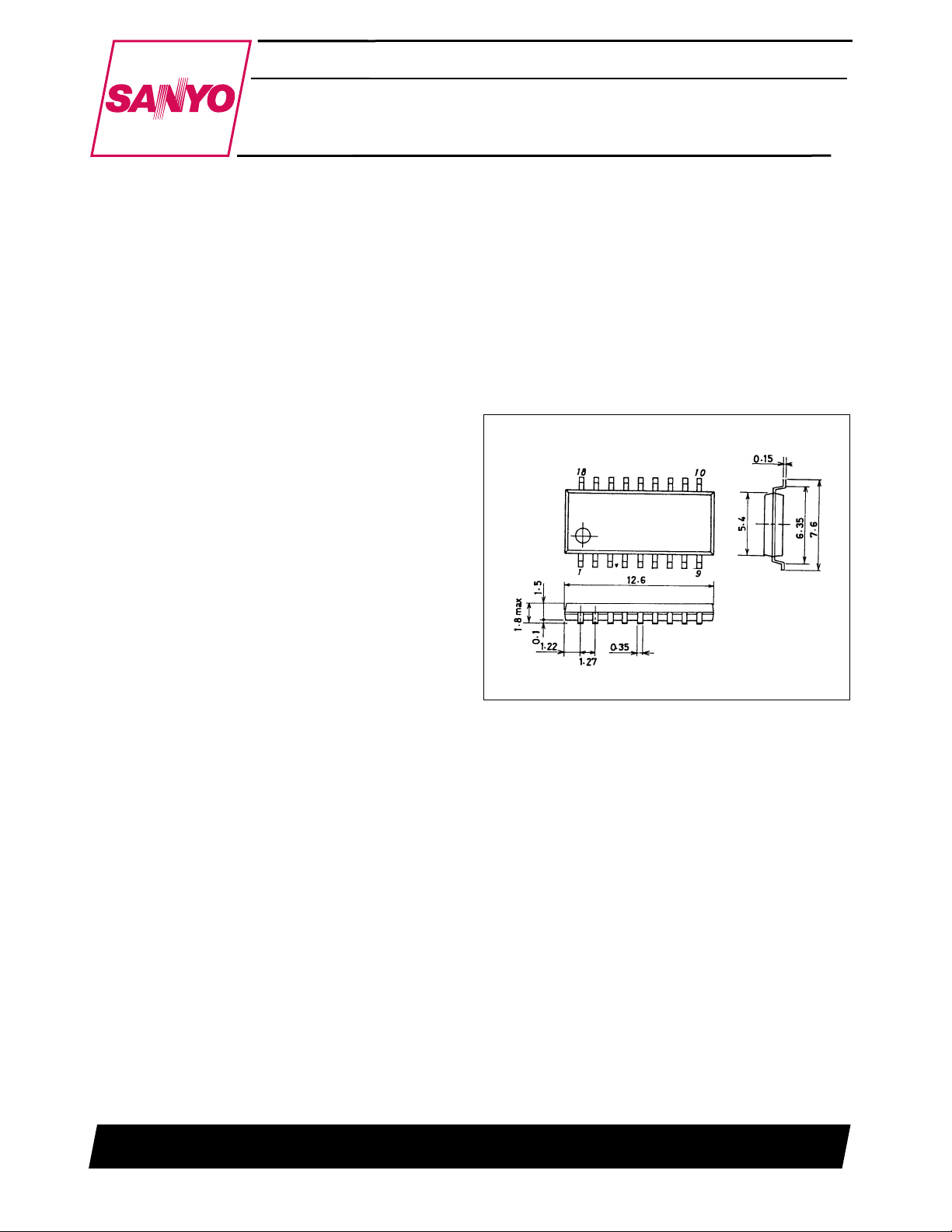
Package Dimensions
unit: mm
3095-MFP18
[LC73701M]
= 2.0 to 5.5 V
DD
SANYO: MFP18
SANYO Electric Co.,Ltd. Semiconductor Bussiness Headquarters
TOKYO OFFICE Tokyo Bldg., 1-10, 1 Chome, Ueno, Taito-ku, TOKYO, 110 JAPAN
53197HA(OT) No. 5561-1/11
Page 2
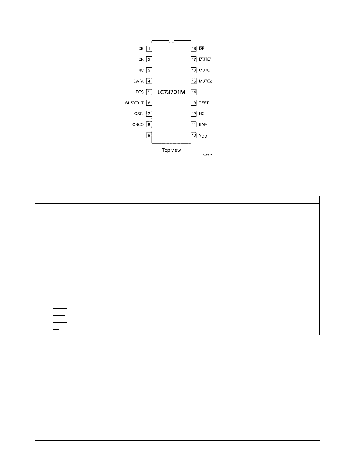
Pin Assignment
LC73701M
DTMF
V
SS
Pin Functions
Pin No. Pin I/O Pin function
1 CE I Set high when data is valid. This signal is also used when DTMF signals are issued consecutively in DTMF mode. The last
2 CK I Data acquisition clock. Data is acquired on the rising edge of this signal.
3NC
4 DATA I Input for the 8-bit data.
5 RES I Reset input. Apply a low level to this input to reset dialer operation when, for example, power is first applied.
6 BUSYOUT O Outputs a high level during dialer operation, including during pauses. This is a complementary output.
7 OSCI I
8 OSCO O
9V
SS
10 V
DD
11 BMR I Make ratio switching input. High: 33%, Low: 39%
12 NC
13 TEST I LSI internal test pin. This pin either must be left open or must be tied low during normal operation.
14 DTMF O DTMF output. This is an npn emitter-follower output.
15 MUTE2 O DTMF mute output. This is an n-channel open-drain output.
16 MUTE O DP and DTMF mute output. This is an n-channel open-drain output.
17 MUTE1 O DP mute output. This is an n-channel open-drain output.
18 DP O DP output. This can be either an n-channel open-drain output or a complementary output.
Unused inputs must always be tied to an appropriate logic level, i.e. either ground or VDD.
DTMF signal is output until CE goes low.
Oscillator circuit connections. Connect either a crystal or ceramic 4.194304 MHz oscillator element to these pins.
Power supply
No. 5561-2/11
Page 3
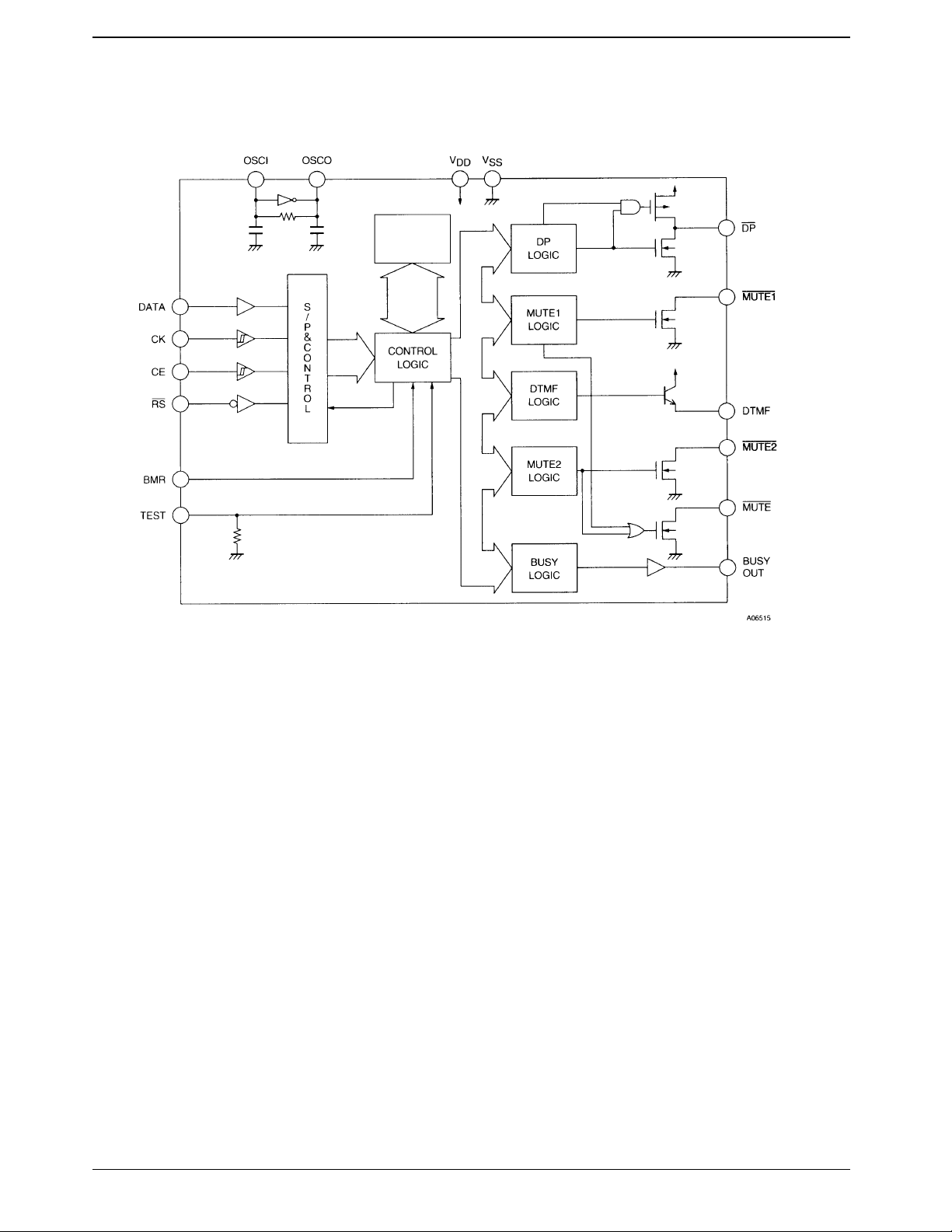
Block Diagram
LC73701M
RAM
5 bits × 32 digits
No. 5561-3/11
Page 4

Input Code Table
LC73701M
D7 D6 D5 D4 D3 D2 D1 D0
X 0 0 0 0 0 0 0 YES KEY D
X 0 0 0 0 0 0 1 YES KEY 1
X 0 0 0 0 0 1 0 YES KEY 2
X 0 0 0 0 0 1 1 YES KEY 3
X 0 0 0 0 1 0 0 YES KEY 4
X 0 0 0 0 1 0 1 YES KEY 5
X 0 0 0 0 1 1 0 YES KEY 6
X 0 0 0 0 1 1 1 YES KEY 7
X 0 0 0 1 0 0 0 YES KEY 8
X 0 0 0 1 0 0 1 YES KEY 9
X 0 0 0 1 0 1 0 YES KEY 0
X 0 0 0 1 0 1 1 YES KEY *
X 0 0 0 1 1 0 0 YES KEY #
X 0 0 0 1 1 0 1 YES KEY A
X 0 0 0 1 1 1 0 YES KEY B
X 0 0 0 1 1 1 1 YES KEY C
X 0 0 1 0 0 0 0 NO Illegal value
X 0 0 1 0 0 0 1 NO Illegal value
X 0 0 1 0 0 1 0 NO PAUSE clear (Only valid during a pause.)
X 0 0 1 0 0 1 1 NO FLASH (707 or 277 ms)
X 0 0 1 0 1 0 0 NO STOP (Forced termination of a the current dialing operation.)
X 0 0 1 0 1 0 1 NO RD (redial)
X 0 0 1 0 1 1 0 NO MUTE ST
X 0 0 1 0 1 1 1 NO MUTE END
X 0 0 1 1 0 0 0 NO ON-HOOK
X 0 0 1 1 0 0 1 NO OFF-HOOK
X 0 0 1 1 1 0 0 YES MODE-CH (Pulse to tone single-direction change)
X 0 0 1 1 1 0 1 YES PAUSE (Pause for either 2.0 or 4.0 seconds.)
WRITE
TO RAM
Data interpretation and notes
X : Don’t care
Only bits D0 to D4 are written to RAM.
Mode Settings Command Table
D7 D6 D5 D4 D3 D2 D1 D0
X MODE TEST DPSEL PAUSE FLASH P/T DPR
X (1) (0) (0) N-CH OD (0) 4.0 s (0) 707.0 ms (0) Tone (0) 20 pps
X (1) (0) (0) CMP (1) 2.0 s (1) 277.3 ms (1) Pulse (1) 10 pps
Flash time Hooking pause time
707.0 ms..................800.8 ms
277.3 ms..................1.23 s
Note that a hooking pause of 804.7 ms is also inserted automatically on a DP-off operation.
No. 5561-4/11
Page 5

LC73701M
Mode Settings at Power On
When power is first applied, the initial settings listed in the table below are established according to the state of the BMR
pin.
BMR PIN DPSEL PAUSE FLASH P/T DPR
H (33.3%) (0) N-CH OD (0) 4.0 s (0) 707.0 ms (1) Pulse (1) 10 pps
L (39.2%) (0) N-CH OD (0) 4.0 s (0) 707.0 ms (0) Tone (1) 10 pps
Specifications
Absolute Maximum Ratings at Ta = 25°C, f
Parameter Symbol Conditions Ratings Unit
Maximum supply voltage V
Maximum input voltage V
Maximum output voltage V
Allowable power dissipation Pd max Ta ≤ 70°C 180 mW
Minimum load resistance R
Operating temperature Topr –30 to +70 °C
Storage temperature Tstg –40 to +125 °C
max –0.3 to +6.5 V
DD
max –0.3 to VDD+0.3 V
IN
max –0.3 to VDD+0.3 V
OUT
min Between the DTMF and the VSSpins 1 kΩ
L
= 4.194304 MHz
OSC
Allowable Operating Ranges at Ta = 25°C, f
Parameter Symbol Conditions
V
Supply voltage
Input high-level voltage
Input low-level voltage
Oscillator pin rating
Electrical Characteristics at Ta = 25°C, f
Parameter Symbol Conditions
Quiescent current drain I
Memory retention voltage V
Memory retention current I
Input pin current I
Output pin leakage current I
Output pin voltage
DDP
V
DDT
V
IHS
V
IH
V
ILS
V
IL
f Center frequency = 4.194304 MHz –1.4 +1.4 %
R
S
OSC
I
DDP
DDT
I
DD(ST)
DR
DR
I
IHI
ILI
I
IHIT
I
ILITVIL
OFF
V
OH1VDD
V
OH2
V
OL1
V
OL2
= 4.194304 MHz
OSC
Ratings
min typ max
Unit
Pulse mode 1.5 5.5 V
DTMF mode 2.0 5.5 V
CK and CE input pins 0.8 V
Input pins other than CK and CE 0.7 V
CK and CE input pins V
Input pins other than CK and CE V
DD
DD
SS
SS
0.2 V
0.3 V
V
DD
V
DD
DD
DD
100 Ω
= 4.194304 MHz
Ratings
min typ max
In dial pulse output mode, output open
V
= 3.0 V : V
DD
DD
0.3 0.5 mA
In DTMF output mode, output open, 0.5 1.0 mA
= 3.0 V: V
V
DD
DD
Standby mode, output open
V
= 1.5 to 5.5 V : V
DD
Between VDDand VSS: V
VDD= 1.0 V : V
DD
DD
DD
1V
VIH= VDD, VDD= 5.5 V : DATA, CK, CE,
BMR, RS
VIL= VSS, VDD= 5.5 V : DATA, CK, CE,
BMR, RS
–1 µA
VIH= VDD, VDD= 5.5 V : TEST 160 330 µA
= VSS, VDD= 5.5 V : TEST –1 µA
VOH= VDD, VDD= 5.5 V, when the output is
off: BUSYOUT
= 1.5 V, IOH= –250 µA : BUSYOUT VDD–0.5 V
VDD= 5.5 V, IOH= –1 mA : BUSYOUT, DP,
MUTE1, MUTE2, MUTE V
DD
–1
VDD= 1.5 V, IOL= 250 µA : BUSYOUT, DP,
MUTE1, MUTE2, MUTE
VDD= 5.5 V, IOL= 1 mA : BUSYOUT, DP,
MUTE1, MUTE2, MUTE
Unit
1µA
0.5 µA
1µA
1µA
0.4 V
0.4 V
V
V
V
V
V
No. 5561-5/11
Page 6

LC73701M
Dialer Input Format
The serial data is input starting with the LSB.
T1 must be at least 6.5 µs (When an external clock is supplied to OSC1.)
If an oscillator element is used, T1 depends on the oscillator startup time for that oscillator element.
*: For example, for ceramic oscillators, T1 will be about 1 ms (VDD= 3.0 to 5.5 V).
T2 and T3 must be at least 1.0 µs.
Serial Data Sequential Input Format
*: Continuous input is limited to dial data. Continuous input of mode setting commands is not possible.
Mode Settings Format
Point when the DTMF output for KEY32 goes off
KEY1 to KEY31 are guaranteed by the DTMF output time.
Don’t care
A06518
No. 5561-6/11
Page 7

Timing Charts
(1) Pulse mode
(2) Tone mode
DTMF output
DP output
LC73701M
AC Characteristics at Ta = 25°C, f
Parameter Symbol Conditions
Pause time T
DTMF output time T
DTMF inter-digit pause time T
Flash time T
Hooking pause time T
Low tone amplitude V
Tone output ratio dBCR V
Tone output distortion %DIS V
Pulse Output at Ta = 25°C, f
DPR BMR Dial pulse rate Pre-digit pause Inter-digit pause Make ratio
H H 9.97 PPS 33.3 + 10 ms 839.0 ms 33.3%
H L 9.97 PPS 39.2 + 10 ms 844.9 ms 39.2%
L H 19.93 PPS 16.7 + 10 ms 571.6 ms 33.3%
L L 19.93 PPS 19.7 + 10 ms 574.6 ms 39.2%
OSC
DTMF Output Frequencies at Ta = 25°C, f
Output frequency (Hz)
Input
Rating LC73701
R1 697 697.2 +0.027
R2 770 769.9 –0.016
R3 852 851.8 –0.023
R4 941 941.3 +0.029
C1 1209 1209.4 +0.036
C2 1336 1335.8 –0.018
C3 1477 1476.9 –0.009
C4 1633 1633.3 +0.018
Deviation (%)
= 4.194304 MHz
OSC
When the D3 mode setting code is low (0) 4.0 s
AP
When the D3 mode setting code is high (1) 2.0 s
MFON
For the first and later digits 114.0 ms
MFOFF
For the last digit 109.9 ms
When the D2 mode setting code is low (0) 707.0 ms
FL
When the D2 mode setting code is high (1) 277.3 ms
When the D2 mode setting code is low (0) 800.8 ms
HKP
When the D2 mode setting code is high (1) 1.23 s
ORVDD
= 3.5 V, RL= 10 kΩ 165 200 240 mVrms
= 2.0 to 5.5 V, RL= 10 kΩ 1 2 3 dB
DD
= 2.0 to 5.5 V, RL= 10 kΩ 10 %
DD
= 4.194304 MHz
OSC
= 4.194304 MHz
Ratings
min typ max
100.6 ms
Unit
No. 5561-7/11
Page 8

LC73701M
Internal Pin Circuits
Pin No. Pin Internal circuit
1
2
4
5
11
6
18
7 OSCI
CE
CK
DATA
RES
BMR
BUSYOUT
DP
8 OSCO
15
16
17
13 TEST
MUTE2
MUTE
MUTE1
Continued on next page.
No. 5561-8/11
Page 9

LC73701M
Continued from preceding page.
Pin No. Pin Internal circuit
14 DTMF
18 DP
Notes:
(1) The LC73701M output ports are initialized to the following states when power is first applied.
BUSYOUT and DP pins: Low
DTMF, MUTE1, MUTE, and MUTE2 pins: High-impedance
OSC0 pin: High
(2) The following methods can be used to forcibly terminate dial output.
1. STOP command input
Output ports: The DP and MUTE1 pins hold their previous states, all others are initialized.
Redialing is possible after a STOP command is input. However, this requires that a dialing operation had been
performed previously.
2. Applying a low-level pulse (of at least 1 µs) to the RES pin.
The operation is identical to that of the STOP command.
However, redialing is not possible after this hardware reset.
3. ON-HOOK command input
The DP pin goes low, thus releasing the telephone line (circuit). Redialing is possible after an ON-HOOK
command is input. However, if this dialing operation is performed, although DTMF signals will be output, since
the DP is low dial pulses will not be output. (Since the LSI performs a redial operation internally, the BUSYOUT
pin will go high and the associated muting signal will also be output.)
4. OFF-HOOK command input
A hooking pause will be inserted automatically after the OFF-HOOK command input. Redialing is possible.
5. FLASH command input
A hooking pause will be inserted automatically after the FLASH command input. Redialing is possible.
(3) The MUTE ST and MUTE END commands
These commands allows the MUTE1 pin to be controlled arbitrarily. The other muting outputs cannot be controlled
explicitly.
The figure below shows the timing.
When a MUTE ST command is input, the MUTE1 pin goes low. During this low period, inputting pulse dial data
will not cause the MUTE1 pin to return to the high level. That is, the low level is held until the next MUTE END
command is input.
No. 5561-9/11
Page 10

LC73701M
(4) The ON-HOOK and OFF-HOOK commands
These commands allows the DP pin to be controlled arbitrarily. The figure below shows the timing.
A hooking pause is inserted automatically when the OFF-HOOK command is input. The DP pin goes low when an
ON-HOOK command is input. During this low period, inputting pulse dial data will not cause the DP pin to return to
the high level. (Since the LSI performs a redial operation internally, the BUSYOUT pin will go high.) That is, the
low level is held until the next OFF-HOOK command is input.
(5) The redial command
The redial operation re-outputs the dial data in the LC73701M’s internal buffer memory. This buffer memory (redial
memory) can hold up to 32 digits of dialing data. This means that if 33 or more digits of dialing data are input, earlier
data will be overwritten starting with the thirty-third digit. After the following operations, the LC73701M will
perform a redial operation if a redial command is input.
1. When a flash command is input after dialing data has been input
2. When an STOP command is input after dialing data has been input
3. When an ON-HOOK command is input after dialing data has been input
4. When an OFF-HOOK command is input after dialing data has been input
(6) Mode settings
The break/make ratio (BMR) is switched between 33% and 39% by the BMR pin. The BMR pin is initialized after
power is first applied as shown in the table below.
BMR PIN DPSEL PAUSE FLASH P/T DPR
H (33.3%) (0) N-CH OD (0) 4.0 s (0) 707.0 ms (1) Pulse (1) 10 pps
L (39.2%) (0) N-CH OD (0) 4.0 s (0) 707.0 ms (0) Tone (1) 10 pps
Settings other than BMR (i.e. DPR, P/T, FLASH, PAUSE, and DPSEL) are switched using mode commands. The
information set by mode setting commands is stored internally by the LSI. Set the desired mode before inputting dial
data. When dial data is written to the buffer memory, the P/T register data is attached to that dial data.
(7) Output pins during dialing and the redial operation
See the table below. The terms ON and OFF in the table below refer to the on or off state of the n-channel open drain
output transistor.
DP MUTE1 MUTE, MUTE2 BUSYOUT Redial memory
Power on ON (L) OFF OFF L Readout is illegal
RES pin ON (L) *1 OFF OFF L Readout is illegal
STOP command *2 OFF (H) *3 OFF OFF L Readout allowed
ON-HOOK command ON (L) Retains the previous state OFF L Readout allowed
OFF-HOOK command OFF (H) Retains the previous state OFF *4 H Readout allowed
MUTE-ST command Retains the previous state ON OFF L Readout allowed
MUTE-END command Retains the previous state OFF OFF L Readout allowed
Notes: *2 Turned off during dialing. However, since this command takes priority after an OFF-HOOK command is input, the on state is retained.
*1, 3: Turned off during dialing. However, since this command takes priority after a MUTE-ST command is input, the on state is retained.
*4: Since a hooking pause is inserted automatically, this output goes high during that operation.
No. 5561-10/11
Page 11

LC73701M
(8) CE input format (When an oscillator element is used.)
The figure below shows the CE timing.
Although in the timing shown in the previous figure, T1 depends on the oscillator element startup time, here, this
time does not need to be provided in the T1 period as long as it can be provided by the T4 period. For example,
assume that the oscillator startup time when a ceramic oscillator is used is about 1 ms (when VDD= 3.0 to 5.5 V). In
this case, this time must be provided by either setting T1 = 1 ms, or by setting T4 = 1 ms. However, note that T1
must be 6.5 µs or greater and T4 must be 1 µs or greater.
■ No products described or contained herein are intended for use in surgical implants, life-support systems, aerospace
equipment, nuclear power control systems, vehicles, disaster/crime-prevention equipment and the like, the failure of
which may directly or indirectly cause injury, death or property loss.
■ Anyone purchasing any products described or contained herein for an above-mentioned use shall:
➀ Accept full responsibility and indemnify and defend SANYO ELECTRIC CO., LTD., its affiliates, subsidiaries and
distributors and all their officers and employees, jointly and severally, against any and all claims and litigation and all
damages, cost and expenses associated with such use:
➁ Not impose any responsibility for any fault or negligence which may be cited in any such claim or litigation on
SANYO ELECTRIC CO., LTD., its affiliates, subsidiaries and distributors or any of their officers and employees
jointly or severally.
■ Information (including circuit diagrams and circuit parameters) herein is for example only; it is not guaranteed for
volume production. SANYO believes information herein is accurate and reliable, but no guarantees are made or implied
regarding its use or any infringements of intellectual property rights or other rights of third parties.
This catalog provides information as of May, 1997. Specifications and information herein are subject to change
without notice.
No. 5561-11/11
 Loading...