

Page 1
Overview
The LC72P366 is a single-chip PLL-plus-controller onetime programmable PROM microcontroller that
corresponds to the Sanyo LC72358N, LC72362N, and
LC72366. The LC72P366 has the same package and pin
assignment as the LC72358N, LC72362N, and LC72366
mask ROM versions, and provides 32 KB of on-chip
PROM, organized as 16k words by 16 bits. The
LC72P366 can prove useful in reducing the startup times
for initial production runs and for reducing the switchover
time when end-product specifications change.
Features
• 32 KB (16k words × 16 bits) of on-chip PROM
— This is a one-time programmable 32 KB (16k-word
× 16-bit) PROM.
• Pin compatible with the mask ROM versions, i.e.
identical package and pin assignment.
Writing Sanyo ROMs
Sanyo provides a for-fee ROM writing service that
consists of writing data to the PROM in one-time
programmable PROM microcontrollers, printing,
screening, and data readout verification. Contact your
Sanyo sales representative for details.
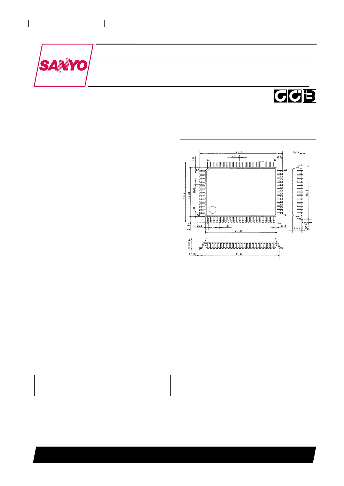
Package Dimensions
unit: mm
3174-QFP80E
CMOS LSI
Ordering number :EN5544
N3096HA (OT) No. 5544-1/14
SANYO: QIP80E
[LC72P366]
SANYO Electric Co.,Ltd. Semiconductor Bussiness Headquarters
TOKYO OFFICE Tokyo Bldg., 1-10, 1 Chome, Ueno, Taito-ku, TOKYO, 110 JAPAN
On-Chip One-Time Programmable PROM
Single-Chip PLL Controller
LC72P366
• CCB is a trademark of SANYO ELECTRIC CO., LTD.
• CCB is SANYO’s original bus format and all the bus
addresses are controlled by SANYO.
Page 2
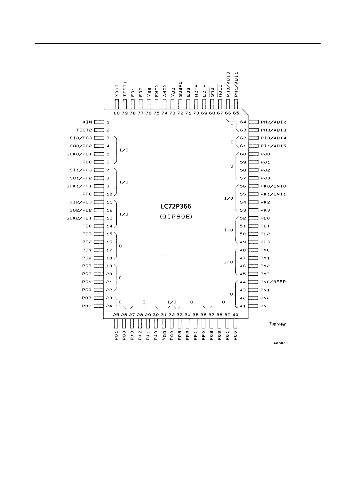
Pin Assignment
No. 5544-2/14
LC72P366
Page 3
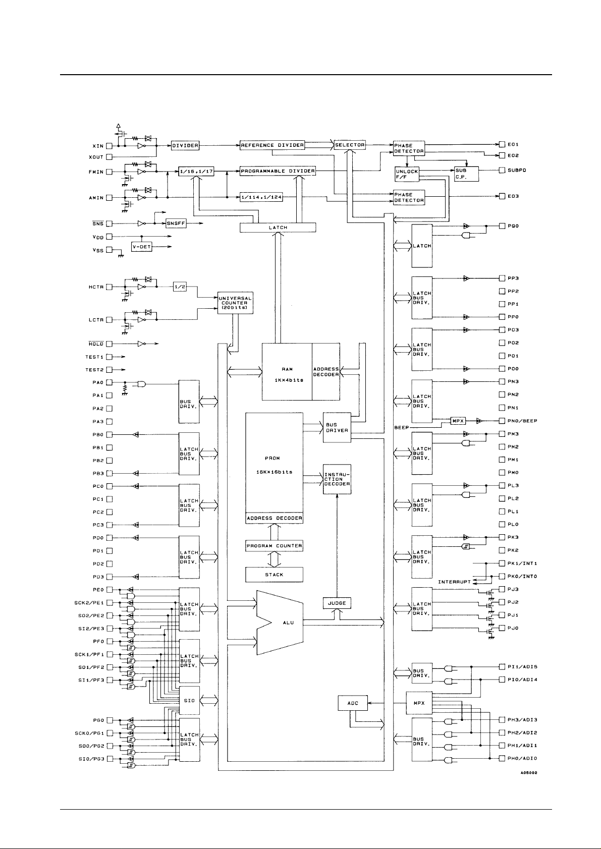
Block Diagram
No. 5544-3/14
LC72P366
Page 4
No. 5544-4/14
LC72P366
Parameter Symbol Conditions Ratings Unit
Maximum supply voltage V
DD
max –0.3 to +6.5 V
Input voltage V
IN
All input pins –0.3 to VDD+0.3 V
Output voltage
V
OUT
(1) Port J –0.3 to +15 V
V
OUT
(2) All output ports other than V
OUT
(1) –0.3 to VDD+0.3 V
I
OUT
(1) Port J 0 to +5 mA
Output current I
OUT
(2)
Ports D, E, F, G, K, L, M, N, O, P, and Q, EO1, EO2, EO3, SUBPD
0 to +3 mA
I
OUT
(3) Ports B and C 0 to +1 mA
Allowable power dissipation Pd max Ta = –30 to +70˚C 400 mW
Operating temperature Topr –30 to +70 ˚C
Storage temperature Tstg –45 to +125 ˚C
Specifications
Absolute Maximum Ratings at Ta = 25˚C, VSS= 0 V
Parameter Symbol Conditions
Ratings
Unit
min typ max
V
DD
(1) CPU and PLL circuit operating 4.5 5.0 5.5 V
Supply voltage V
DD
(2) CPU operating 4.0 5.5 V
V
DD
(3) Memory retention voltage 1.3 5.5 V
V
IH
(1)
Ports E, H, I, L, M, and Q, HCTR,
0.7 V
DD
V
DD
V
LCTR (when selected for input)
Input high-level voltage VIH(2)
Ports F, G, and K,
0.8 V
DD
V
DD
V
LCTR (in period measurement mode), HOLD
V
IH
(3) SNS 2.5 V
DD
V
V
IH
(4) Port A 0.6 V
DD
V
DD
V
V
IL
(1)
Ports E, H, I, L, M, and Q, HCTR,
0 0.3 V
DD
V
LCTR (when selected for input)
Input low-level voltage VIL(2)
Ports A, F, G, and K,
0 0.2 V
DD
V
LCTR (in period measurement mode)
V
IL
(3) SNS 0 1.3 V
V
IL
(4) HOLD 0 0.4 V
DD
V
f
IN
(1) XIN 4.0 4.5 5.0 MHz
f
IN
(2) FMIN : VIN(2), VDD(1) 10 150 MHz
f
IN
(3) FMIN : VIN(3), VDD(1) 10 130 MHz
f
IN
(4) AMIN(H) : VIN(3), VDD(1) 2.0 40 MHz
Input frequency f
IN
(5) AMIN(L) : VIN(3), VDD(1) 0.5 10 MHz
f
IN
(6) HCTR : VIN(3), VDD(1) 0.4 12 MHz
f
IN
(7) LCTR : VIN(3), VDD(1) 100 500 kHz
f
IN
(8)
LCTR (in period measurement mode):
1 20 × 10
3
Hz
V
IH
(2), VIL(2), VDD(1)
V
IN
(1) XIN 0.5 1.5 Vrms
Input amplitude V
IN
(2) FMIN 0.10 1.5 Vrms
V
IN
(3) FMIN, AMIN, HCTR, LCTR 0.07 1.5 Vrms
Input voltage range V
IN
(4) ADI0 to ADI5 0 V
DD
V
Allowable Operating Ranges at Ta = –30 to +70˚C, VDD= 3.5 to 5.5 V
Page 5
No. 5544-5/14
LC72P366
Parameter Symbol Conditions
Ratings
Unit
min typ max
I
IH
(1) XIN : VI= VDD= 5.0 V 2.0 5.0 15 µA
I
IH
(2) FMIN, AMIN, HCTR, LCTR : VI= VDD= 5.0 V 4.0 10 30 µA
Ports A, E, F, G, H, I, K, L, M, and Q,
SNS, HOLD,
HCTR, LCTR, and
with no
Input high-level current
I
IH
(3) pull-down resistor on
port A, VI= VDD= 5.0 V
3.0 µA
With input mode selected for ports
E, F, G, K, L, M, and Q
I
IH
(4) Port A: pull-down resistor present 50 µA
I
IL
(1) XIN:VI= V
SS
2.0 5.0 15 µA
I
IL
(2) FMIN, AMIN, HCTR, LCTR : V
SS
4.0 10 30 µA
Ports A, E, F, G, H, I, K, L, M, and Q,
Input low-level current SNS, HOLD, HCTR, LCTR, and with no
I
IL
(3) pull-down resistor on port A, VI= V
SS
3.0 µA
With input mode selected for ports E, F,
G, K, L, M, and Q
Input floating voltage V
IF
Port A: pull-down resistor present 0.05 V
DD
V
Pull-down resistance
R
PD
(1) Port A: pull-down resistor present VDD= 5 V 75 100 200 kΩ
R
PD
(2) TEST1, TEST2 10 kΩ
Hysteresis V
H
Ports F, G, and K, LCTR (in period measurement mode)
0.1 V
DD
0.2 V
DD
V
V
OH
(1) Ports B and C: IO= –1 mA
VDD– 2.0 VDD– 1.0
V
Output high-level voltage
V
OH
(2)
Ports D, E, F, G, K, L, M, N, O, P, and Q: I
O
= –1 mA
VDD– 1.0
V
V
OH
(3) EO1, EO2, EO3, SUBPD : IO= –500 µA
VDD– 1.0
V
V
OH
(4) XOUT : IO= –200 µA
VDD– 1.0
V
V
OL
(1) Ports B and C: IO= 50 µA 1.0 2.0 V
V
OL
(2)
Ports D, E, F, G, K, L, M, N, O, P, and Q: I
O
= 1 mA
1.0 V
Output low-level voltage V
OL
(3) EO1, EO2, EO3, SUBPD : IO= 500 µA 1.0
V
OL
(4) XOUT : IO= 200 µA 1.5
V
OL
(5) Port J: IO= 5 mA 2.0 V
I
OFF
(1)
Ports B, C, D, E, F, G, K, L, M, N, O, P, and Q
–3.0 +3.0 µA
Output off leakage current I
OFF
(2) EO1, EO2, EO3, SUBPD –100 +100 nA
I
OFF
(3) Port J –5.0 +5.0 µA
A/D conversion error ADI0 to ADI5 : V
DD
(1) –1/2 +1/2 LSB
Rejected pulse width P
REJ
SNS 50 µs
Power down detection voltage V
DET
3.0 3.5 4.0 V
I
DD
(1) VDD(1) : fIN(2) = 130 MHz, Ta = 25˚C 12 24 mA
I
DD
(2) VDD(2): halt mode*, Ta = 25˚C (See figure 1.) 0.45 mA
Current drain I
DD
(3)
V
DD
= 5.5 V, oscillator stopped
5 µA
Ta = 25˚C (See figure 2.)
I
DD
(4)
V
DD
= 2.5 V, oscillator stopped
1 µA
Ta = 25°C (See figure 2.)
Electrical Characteristics in the Allowable Operating Ranges
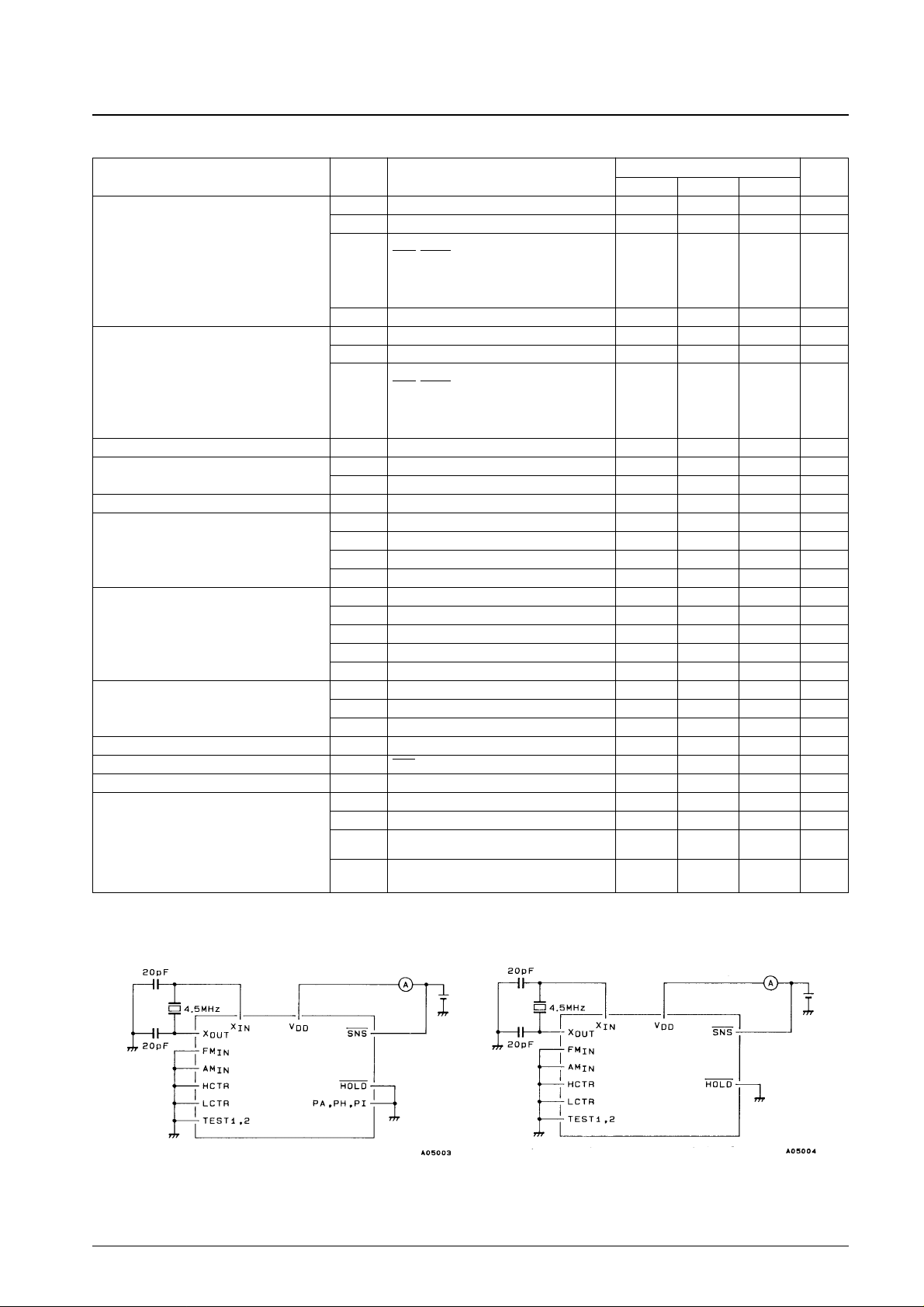
Note: * Executing 20 STEP instructions every millisecond. With the PLL and counter circuits stopped.
Note: With PB to PG, and PJ to PQ all open.
However, with PE to PG, PK to PM, and PQ selected for output.
Figure 1 IDD(2) in Halt Mode
Note: With PA to PQ all open.
Figure 2 IDD(3) and IDD(4) in Backup Mode
Test Circuit Diagrams
Page 6

No. 5544-6/14
LC72P366
Pin Functions
Pin No. Symbol I/O I/O type Function
30
29
28
27
26
25
24
23
22
21
20
19
18
17
16
15
14
13
12
11
10
9
8
7
6
5
4
3
1
80
78
77
PA0
PA1
PA2
PA3
PB0
PB1
PB2
PB3
PC0
PC1
PC2
PC3
PD0
PD1
PD2
PD3
PE0
PE1/SCK2
PE2/SO2
PE3/SI2
PF0
PF1/SCK1
PF2/SO1
PF3/SI1
PG0
PG1/SCK0
PG2/SO0
PG3/SI0
XIN
XOUT
EO1
EO2
I
O
O
I/O
I
O
O
Pull-down resistor
included Input
Unbalanced CMOS
push-pull
CMOS push-pull
CMOS push-pull
—
CMOS tristate
Key return signal input-only ports. The threshold voltage is set to a relatively low value.
When a key matrix is formed in combination with the PB and PC ports, up to three
simultaneous key presses can be detected.
The pull-down resistors are set by the IOS instruction with PWn = 2 for all four pins at the
same time and cannot be set on an individual pin basis.
Input is disabled in clock stop mode.
Key source signal output-only ports. Since the output transistor circuit is an unbalanced
CMOS structure, diodes to prevent shorting due to multiple key presses are not required.
In clock stop mode, these pins go to the output high-impedance state.
During the power-on reset, these pins go to the output high-impedance state and hold that
state until an output instruction is executed.
Output-only ports.
In clock stop mode, these pins go to the output high-impedance state.
During the power-on reset, these pins go to the output high-impedance state and hold that
state until an output instruction is executed.
General-purpose I/O port/serial I/O pin shared-function ports.
The F and G port inputs are Schmitt inputs. The E ports is a normal input.
The IOS instruction switches these ports between general-purpose I/O ports and serial I/O
ports, and between input and output for general-purpose I/O ports.
• When used as general-purpose I/O ports these pins:
Can be set for input or output in bit units (bit I/O), and
are set for use as general-purpose I/O ports by the IOS instruction with PWn = 0.
b0 = SI/O 0 0 ...................general-purpose port
b1 = SI/O 1 1 ...................SI/O port
b2 = SI/O 2
are set for input or output by the IOS instruction in bit units.
PE..............PWn = 4 0 ...................Input
PF..............PWn = 5 1...................Output
PG.............PWn = 6
• When used as serial I/O ports these pins:
Are set for serial I/O port use by the IOS instruction with PWn = 0, and
are accessed by reading and writing the serial I/O data buffer with the INR and OUTR
instructions.
Note: Pin setup states when used as serial I/O ports:
PE0, PF0, PG0......General-purpose I/O
PE1, PF1, PG1......SCK output in internal clock mode
SCK input in external clock mode
PE2, PF2, PG2......SO output
PE3, PF3, PG3......SI input
In clock stop mode, input is disabled and these pins go to the high-impedance state.
During the power-on reset, these pins become general-purpose input ports.
Connections for a 4.5 MHz crystal oscillator
Main charge pump outputs
These pins output a high level when the frequency generated by dividing the local
oscillator signal frequency by N is higher than the reference frequency, and a low level
when that frequency is lower.
These pins go to the high-impedance state when the frequencies match.
These pins go to the high-impedance state when the HOLD pin is set low in the hold
enable state.
In clock stop mode, during the power-on reset and in the PLL stop state, these pins go to
the high-impedance state.
Continued on next page.
Page 7

No. 5544-7/14
LC72P366
Continued from preceding page.
Continued on next page.
Pin No. Symbol I/O I/O type Function
76
73
31
75
74
72
71
V
SS
V
DD
V
DD
FMIN
AMIN
SUBPD
EO3
—
I
I
O
O
—
Input
Input
CMOS tristate
CMOS tristate
Power supply connections
FM VCO (local oscillator) input
This pin is selected by the PLL instruction CW1 (b1, b0 are ignored).
Capacitor coupling must be used for signal input.
Input is disabled when the HOLD pin is set low in the hold enable state.
Input is disabled in clock stop mode, during the power-on reset, and in the PLL stop state.
AM VCO (local oscillator) input
This pin is selected and the band set by the PLL instruction CW1 (b1, b0).
Capacitor coupling must be used for signal input.
Input is disabled when the HOLD pin is set low in the hold enable state.
Input is disabled in clock stop mode, during the power-on reset, and in the PLL stop state.
Sub-charge pump output
This pin, in combination with the main charge pump, allows the construction of a highspeed locking circuit.
The DZC instruction controls the sub-charge pump.
This pin goes to the high-impedance state when the HOLD pin is set low in the hold enable
state.
This pin goes to the high-impedance state in clock stop mode, during the power-on reset,
and in the PLL stop state.
Second PLL charge pump output
This pin outputs a low level when the frequency generated by dividing the local oscillator
signal frequency by N is higher than the reference frequency, and a high level when that
frequency is lower.
This pin goes to the high-impedance state when the frequencies match. (Note that this
pin’s output logic is the opposite of that of the EO1 and EO2 pins.)
This pin goes to the high-impedance state when the HOLD pin is set low in the hold enable
state.
This pin goes to the high-impedance state in clock stop mode, during the power-on reset,
and in the PLL stop state.
b1 b0 Band
1 0 2 to 40 MHz (SW)
1 1 0.5 to 10 MHz (MW, LW)
b3 b2 Operation
0 0 High impedance
0 1 Only operates in the unlocked state (450 kHz)
1 0 Only operates in the unlocked state (900 kHz)
1 1 Normal operation
Page 8

No. 5544-8/14
LC72P366
Continued from preceding page.
Continued on next page.
Pin No. Symbol I/O I/O type Function
70
69
68
HCTR
LCTR
SNS
I
I
I
Input
Input
Input
Universal counter/general-purpose input shared-function input port
The IOS instruction b3 with PWn = 3 switches the pin function between universal counter
input and general-purpose input.
• Frequency measurement
The universal counter function is selected by an IOS instruction with PWn = 3 and b3 = 0.
HCTR frequency measurement mode is set up by a UCS instruction with b3 = 0 and b2 =
0, and counting is started with a UCC instruction after the count time is selected.
The CNTEND flag is set when the count completes.
To operate this circuit as an AC amplifier in this mode, the input must be capacitor
coupled.
• General-purpose input pin use
The general-purpose input port function is selected by an IOS instruction with PWn = 3
and b3 = 1.
An internal register (address: 0EH) input instruction INR (b0) is used to acquire data from
this pin.
Input is disabled in clock stop mode. (The input pin will be pulled down.)
During the power-on reset, the universal counter function is selected.
Universal counter (frequency and period measurement)/general-purpose input sharedfunction input port
The IOS instruction b2 with PWn = 3 switches the pin function between universal counter
input and general-purpose input.
• Frequency measurement
The universal counter function is selected by an IOS instruction with PWn = 3 and b2 = 0.
LCTR frequency measurement mode is set up by a UCS instruction with b3 = 0 b2 = 1,
and counting is started with a UCC instruction after the count time is selected.
The CNTEND flag is set when the count completes.
To operate this circuit as an AC amplifier in this mode, the input must be capacitor
coupled.
• Period measurement
With the universal counter function selected, set up period measurement mode with a
UCS instruction with b3 = 1 and b2 = 0, and start the count with a UCC instruction after
selecting the count time. The CNTEND flag will be set when the count completes. In this
mode, the signal must be input with DC coupling to turn off the bias feedback resistor.
• General-purpose input pin use
The general-purpose input port function is selected by an IOS instruction with PWn = 3,
b2 = 1.
An internal register (address: 0EH) input instruction INR (b1) is used to acquire data from
this pin.
Input is disabled in clock stop mode. (The input pin will be pulled down.)
During the power-on reset, the universal counter function (in HCTR frequency
measurement mode) is selected.
Voltage sense/general-purpose input pin shared-function port
This circuit is designed for a relatively low input threshold voltage.
• Voltage sense pin usage
This input pin is used to determine whether or not a power failure occurred after recovery
from backup (clock stop) mode. An internal sense F/F is used for this determination. The
sense F/F is tested with a TUL instruction (b2).
• General-purpose input port usage
When used as a general-purpose input port, the state is sensed by using a TUL
instruction (b3).
Since, unlike other input ports, input is not disabled in clock stop mode and during the
power-on reset, special care is required with respect to through currents.
Page 9

No. 5544-9/14
LC72P366
Continued from preceding page.
Pin No. Symbol I/O I/O type Function
67
66
65
64
63
62
61
60
59
58
57
56
55
54
53
52 to
45
HOLD
PH0/ADI0
PH1/ADI1
PH2/ADI2
PH3/ADI3
PI0/ADI4
PI1/ADI5
PJ0
PJ1
PJ2
PJ3
PK0/INT0
PK1/INT1
PK2
PK3
PL0 to PL3
PM0 to PM3
I
I
O
I/O
I/O
Input
Input
N-channel open drain
CMOS push-pull
CMOS push-pull
PLL control and clock stop mode control
Setting this pin low in the hold enabled state disables input to the FMIN and AMIN pins and
sets the EO pin to the high-impedance state.
To enter clock stop mode, set the HOLDEN flag, set this pin low, and execute a CKSTP
instruction.
To clear clock stop mode, set this pin high.
General-purpose input port/A/D converter shared-function pins
The IOS instruction with PWn = 7 or 8 switches the pin function between general-purpose
input ports and A/D converter inputs.
• General-purpose input port usage
Specify general-purpose input port usage with the IOS instruction with PWn = 7 or 8 in bit
units.
• A/D converter usage
Specify A/D converter usage with the IOS instruction with PWn = 7 or 8 in bit units.
Specify the pin to convert with the IOS instruction with PWn = 1.
Start a conversion with the UCC instruction (b2).
The ADCE flag will be set when the conversion competes.
Note: Executing an input instruction for a port specified for ADI usage will always return
low since input is disabled. These pins must be set up for general-purpose input
port usage before an input instruction is executed.
Input is disabled in clock stop mode.
During the power-on reset, these pins go to the general-purpose input port function.
General-purpose output ports
An external pull-up resistor is required since these pins are open-drain circuits.
In clock stop mode, these pins go to the transistor off state (high level output).
During the power-on reset, these pins are set up as general-purpose output ports and go
to the transistor off state (high level output).
General-purpose I/O/external interrupt shared-function ports
There is no instruction that switches the function of these ports between general-purpose
ports and external interrupt ports. These pins function as external interrupt pins at the point
where the external interrupt enable flag is set.
• General-purpose I/O port usage
These pins can be set for input or output in bit units (bit I/O).
The IOS instruction is used to specify input or output in bit units.
• External interrupt pin usage
This function can be used by setting the external interrupt enable flags (INT0EN and
INT1EN) in status register 2. The corresponding pin must be set up for input.
To enable interrupt operation, the interrupt enable flag (INTEN) in status register 1 also
must be set.
The IOS instruction with PWn = 3, b1 = INT1, and b0 = INT0 is used to select rising or
falling edge detection.
In clock stop mode, input is disabled and these pins go to the high impedance state.
During the power-on reset, these pins function as general-purpose input ports.
General-purpose I/O ports
The IOS instruction is used to specify input or output.
In clock stop mode input is disabled and these pins go to the high impedance state.
During the power-on reset, these pins function as general-purpose input ports.
Continued on next page.
Page 10

No. 5544-10/14
LC72P366
Usage Notes
The LC72P366 is provided for use in initial shipments of products designed to use the Sanyo LC72358N, LC72362N, or
LC72366. Keep the following points in mind when using this product.
• Differences between the LC72P366 and the LC72358N, LC72362N, and LC72366
• ROM ordering procedure when using Sanyo’s for-fee PROM programming service
— When ordering one-time programmable versions and mask versions at the same time:
The customer must provide the mask ROM version program, the mask ROM version order forms, and the one-time
programmable version order forms.
— When order just the one-time programmable version:
The customer must provide the one-time programmable version program and the one-time programmable version
order forms.
Parameter LC72P366 LC72358N, 72362N, 72366
Operating temperature –30 to +70˚C –40 to +85˚C
Minimum 4.0 V Minimum 3.5 V
CPU operating voltage Typical Typical
Maximum 5.5 V Maximum 5.5 V
Minimum 3.0 V Minimum 2.7 V
Power down detection voltage (VDET) Typical 3.5 V Typical 3.0 V
Maximum 4.0 V Maximum 3.3 V
Continued from preceding page.
Pin No. Symbol I/O I/O type Function
44
43
42
41
40 to
33
32
79
2
PN0/BEEP
PN1
PN2
PN3
PO0 to PO3
PP0 to PP3
PQ0
TEST1
TEST2
O
O
I/O
CMOS push-pull
CMOS push-pull
CMOS push-pull
General-purpose output port/BEEP tone shared-function output pins
The BEEP instruction switches between the general-purpose output port and BEEP tone
functions.
• General-purpose output port usage
The BEEP instruction with b3 = 0 sets up the general-purpose output port function.
Pins PN1 to PN3 are general-purpose output-only pins.
• BEEP output usage
The BEEP instruction with b3 = 1 sets up BEEP output.
The BEEP instruction bits b0, b1 and b2 sets the frequency.
When set up as the BEEP port, executing an output instruction will set the internal latch
data but has no influence on the output.
These pins go to the output high-impedance state in clock stop mode.
These pins go to the output high-impedance state during the power-on reset and hold that
state until an output instruction is executed.
Output-only ports
These pins go to the output high-impedance state in clock stop mode.
These pins go to the output high-impedance state during the power-on reset and hold that
state until an output instruction is executed.
General-purpose I/O ports
The IOS instruction is used to specify input or output.
The OUTR and INR instructions are used for output and input.
The bit set, reset and test instruction cannot be used.
In clock stop mode input is disabled and these pins go to the high impedance state.
During the power-on reset, these pins function as general-purpose input ports.
LSI test pins
These pins must be either left open or connected to ground.
Page 11

• Conditions required for mounting the LC72P366
1. Products programmed by the user:
Mount the LC72P366 using the following procedure
when using products shipped from Sanyo without the
PROM having been programmed.
2. Products programmed by Sanyo:
Mount the LC72P366 using the following procedure
when using products shipped from Sanyo with the
PROM programmed by Sanyo.
[Caution]
• Due to the nature of the product, it is not possible for Sanyo to fully test
one-time programmable PROM microcontrollers (i.e., products with
blank PROMs) before shipment to the customer. This means that there
will be some amount of yield reduction after programming.
No. 5544-11/14
LC72P366
Usage Procedures
• Programming the on-chip PROM
There are two methods for writing the LC72P366 on-chip PROM as follows:
— Using a general-purpose PROM programmer
A general-purpose PROM programmer can be used if a special-purpose PROM programming adapter (product
name: LC72P366 EPROM PROGRAMMER) is used. The write procedure used is the 27512 or 27C512 (with Vpp
= 12.5 V) Intel fast write method. Specify 0000H to 7FFFH as the address settings.
— Using the RE32N in-circuit emulator:
The RE32N in-circuit emulator can be used if a special-purpose PROM programming adapter (product name:
LC72P366 RE32N) is used. Use the PGOTP command as the write method.
• Special-purpose writing adapters
Since there are two special-purpose PROM programming adapters as mentioned above, the correct adapter must be
used.
General-purpose EPROM programmer adapter : Product name LC72P366 EPROM PROGRAMMER
: Catalog no. NDK-DC-018
In-circuit emulator RE32 adapter : Product name LC72P366 RE32N
: Catalog no. NDK-DC-020
Page 12

LC72P366 Instruction Overview
Abbreviations : ADDR : Program memory address
b : Borrow
C : Carry
DH : Data memory address high (Row address) [2 bits]
DL : Data memory address low (Column address) [4 bits]
I : Immediate data [4 bits]
M : Data Memory address
N : Bit position [4 bits]
Pn : Port number [4 bits]
PWn : Port control word number [4 bits]
r : General register (on of location 00 to 0FH in the current bank)
Rn : Register number [4 bits]
( ) : Contents of register or memory
( )n : Contents of bit N of register or memory
No. 5544-12/14
LC72P366
Mnemonic
Operand
Function Operation
Machine code
1st 2nd D15 14 13 12 11 10 9 8 7 6 5 4 3 2 1 D0
AD r M Add M to r r ← (r) + (M) 0 1 0 0 0 0 D
H
D
L
r
ADS r M Add M to r, r ← (r) + (M) 0 1 0 0 0 1 D
H
D
L
r
then skip if carry skip if carry
AC r M Add M to r with carry r ← (r) + (M) + C 0 1 0 0 1 0 D
H
D
L
r
ACS r M Add M to r with carry, r ← (r) + (M) + C 0 1 0 0 1 1 D
H
D
L
r
then skip if carry skip if carry
AI M I Add I to M M ← (M) + I 0 1 0 1 0 0 D
H
D
L
I
AIS M I Add I to M, M ← (M) + I 0 1 0 1 0 1 D
H
D
L
I
then skip if carry skip if carry
AIC M I Add I to M with carry M ← (M) + I + C 0 1 0 1 1 0 D
H
D
L
I
AICS M I Add I to M with carry, M ←(M) + I+ C 0 1 0 1 1 1 D
H
D
L
I
then skip if carry skip if carry
SU r M Subtract M from r r ← (r) – (M) 0 1 1 0 0 0 D
H
D
L
r
SUS r M Subtract M from r, r ← (r) – (M) 0 1 1 0 0 1 D
H
D
L
r
then skip if borrow skip if borrow
SB r M Subtract M from r with r ← (r) – (M) – b 0 1 1 0 1 0 D
H
D
L
r
borrow
SBS r M Subtract M from r with r ← (r) – (M) – b 0 1 1 0 1 1 D
H
D
L
I
borrow, skip if borrow
then skip if borrow
SI M I Subtract I from M M ←(M) – I 0 1 1 1 0 0 D
H
D
L
I
SIS M I Subtract I from M, M ←(M) – I 0 1 1 1 0 1 D
H
D
L
I
then skip if borrow skip if borrow
SIB M I Subtract I from M with M ← (M) – I – b 0 1 1 1 1 0 D
H
D
L
I
borrow
SIBS M I Subtract I from M with M ← (M) – I – b 0 1 1 1 1 1 D
H
D
L
I
borrow, skip if borrow
then skip if borrow
SEQ r M Skip if r equal to M (r) – (M) skip if zero 0 0 0 1 0 0 D
H
D
L
r
SEQI M I Skip if M equal to I (M) – I skip if zero 0 0 0 1 0 1 D
H
D
L
I
SNEI M I Skip if M not equal to I (M) – I skip if not zero 0 0 0 0 0 1 D
H
D
L
I
SGE r M Skip if r is greater than (r) – (M) 0 0 0 1 1 0 D
H
D
L
r
or equal to M skip if not borrow
SGEI M I Skip if M is greater than (M) – I 0 0 0 1 1 1 D
H
D
L
I
or equal to I skip if not borrow
SLEI M I Skip if M is less than I (M) – I skip if zero 0 0 0 0 1 1 D
H
D
L
I
Continued on next page.
Addition instructionsSubtraction instructionsComparison instructions
Instruction
group
Page 13

No. 5544-13/14
LC72P366
Continued from preceding page.
Mnemonic
Operand
Function Operation
Machine code
1st 2n D15 14 13 12 11 10 9 8 7 6 5 4 3 2 1 D0
AND r M AND M with r r ← (r) AND (M) 0 0 1 0 0 0 D
H
D
L
r
ANDI M I AND I with M M ← (M) AND I 0 0 1 0 0 1 D
H
D
L
I
OR r M OR M with r r ← (r) OR (M) 0 0 1 0 1 0 D
H
D
L
r
ORI M I OR I with M M ← (M) OR I 0 0 1 0 1 1 D
H
D
L
r
EXL r M Exclusive OR I with r r ← (r) XOR I 0 0 1 1 0 1 D
H
D
L
r
EXLI M I Exclusive OR I with M M ← (M) XOR I 0 0 1 1 0 1 D
H
D
L
I
SHR r Shift r right with carry carry 0 0 0 0 0 0 0 0 1 1 1 0 r
(r)
LD r M Load M to r r ← (M) 1 1 0 1 0 0 D
H
D
L
r
ST M r Store r to M M ← (r) 1 1 0 1 0 1 D
H
D
L
r
MVRD r M Move M to destinsation [DH, rn] ← (M) 1 1 0 1 1 0 D
H
D
L
r
M referring to r in
the same row
MVRS M r Move M to destinsation M ← [DH, rn] 1 1 0 1 1 1 D
H
D
L
r
M referring to r in
the same row
MVSR M1 M2 Move source M referring [DH, DL1] ← [DH, DL2] 1 1 1 0 0 0 D
H
DL1 DL2
to r to M in the same row
MVI M I Move I to M M ← I 1 1 1 0 0 1 D
H
D
L
I
TMT M N Test M bits, then skip if M (N) = all “1”, 1 1 1 1 0 0 D
H
D
L
N
if all bits specified then skip
are true
TMF M N Test M bits, then skip if M (N) = all “0”, 1 1 1 1 0 1 D
H
D
L
N
if all bits specified then skip
are false
JMP ADDR Jump to the address PC ← ADDR 1 0 ADDR (14 bits)
CAL ADDR Call subroutine Stack ← (PC) + 1 1 1 0 0 ADDR (12 bits)
RT Return from subroutine PC ← Stack 0 0 0 0 0 0 0 0 1 0 0 0
RTS Return from subroutine PC ← Stack + 1 0 0 0 0 0 0 0 0 1 0 1 0
and skip
RTB Return from subroutine PC ← Stack 1 1 1 1 1 1 1 1 1 1 0 0
with bank data BANK ← Stack
RTBS Return from subroutine PC ← Stack + 1 1 1 1 1 1 1 1 1 1 1 0 1
with bank data and skip BANK ← Stack
RTI Return from interrupt PC ← Stack 0 0 0 0 0 0 0 0 1 0 0 1
BANK ← Stack
CARRY ← Stack
SS I N Set status register (Status reg I) N ← 1 1 1 1 1 1 1 1 1 0 0 0 I N
RS I N Reset status register (Status reg I) N ← 0 1 1 1 1 1 1 1 1 0 0 1 I N
TST I N Test status register if (Status reg I) N = 1 1 1 1 1 1 1 1 0 1 I N
true all “1”, then skip
TSF I N Test status register if (Status reg I) N = 1 1 1 1 1 1 1 1 1 0 I N
false “0”, then skip
TUL N Test unlock F/F then if Unlock FF (N) = 0 0 0 0 0 0 0 0 1 1 0 1 N
skip if it has not been all “0”, then skip
set
PLL M r Load M to PLL register PLL reg ← PLL data 1 1 1 1 1 0 D
H
D
L
r
INR M Rn Input register/port M ← (Rn reg) 0 0 1 1 1 0 D
H
D
L
Rn
data to M
OUTR M Rn Output contents of M Rn reg ←(M) 0 0 1 1 1 1 D
H
D
L
Rn
to register/port
Logical instructionsTransfer instructions
Bit test
instructions
Jump and subroutine instructions
Status register
instructions
F/F test
instructions
Internal register
transfer instructions
▲
▲
Continued on next page.
Instruction
group
Page 14

No. 5544-14/14
LC72P366
This catalog provides information as of November, 1996. Specifications and information herein are subject to
change without notice.
■ No products described or contained herein are intended for use in surgical implants, life-support systems, aerospace
equipment, nuclear power control systems, vehicles, disaster/crime-prevention equipment and the like, the failure of
which may directly or indirectly cause injury, death or property loss.
■ Anyone purchasing any products described or contained herein for an above-mentioned use shall:
➀
Accept full responsibility and indemnify and defend SANYO ELECTRIC CO., LTD., its affiliates, subsidiaries and
distributors and all their officers and employees, jointly and severally, against any and all claims and litigation and all
damages, cost and expenses associated with such use:
➁
Not impose any responsibility for any fault or negligence which may be cited in any such claim or litigation on
SANYO ELECTRIC CO., LTD., its affiliates, subsidiaries and distributors or any of their officers and employees
jointly or severally.
■ Information (including circuit diagrams and circuit parameters) herein is for example only; it is not guaranteed for
volume production. SANYO believes information herein is accurate and reliable, but no guarantees are made or implied
regarding its use or any infringements of intellectual property rights or other rights of third parties.
Continued from preceding page.
Mnemonic
Operand
Function Operation
Machine code
1st 2n D15 14 13 12 11 10 9 8 7 6 5 4 3 2 1 D0
SIO I1 I2 Serial I/O control SIO reg ← I1,I2 0 0 0 0 0 0 0 1 I1 I2
UCS I Set I to UCCW1 UCCW1 ← I 0 0 0 0 0 0 0 0 0 0 0 1 I
UCC I Set I to UCCW2 UCCW2 ← I 0 0 0 0 0 0 0 0 0 0 1 0 I
BEEP I Beep control BEEP reg ← I 0 0 0 0 0 0 0 0 0 1 1 0 I
DZC I Dead zone control DZC reg ← I 0 0 0 0 0 0 0 0 1 0 1 1 I
TMS N Set timer register Timer reg ← I 0 0 0 0 0 0 0 0 1 1 0 0 N
IOS PWn N Set port control word IOS reg PWn ← N 1 1 1 1 1 1 1 0 PWn N
IN M Pn Input port data to M M ← (Pn) 1 1 1 0 1 0 D
H
D
L
Pn
OUT M Pn Output contents of M Pn ← M 1 1 1 0 1 1 D
H
D
L
Pn
to port
SPB Pn N Set port bits (Pn) N ← 1 0 0 0 0 0 0 1 0 Pn N
RPB Pn N Reset port bits (Pn) N ← 0 0 0 0 0 0 0 1 1 Pn N
TPT Pn N Test port bit, then skip if (Pn) N = all “1”, 1 1 1 1 1 1 0 0 Pn N
if all bits specified are then skip
true
TPF Pn N Test port bits, then skip if (Pn) N = all “0”, 1 1 1 1 1 1 0 1 Pn N
if all bits specified are then skip
false
BANK I Select Bank BANK ← I 0 0 0 0 0 0 0 0 0 1 1 1 I
HALT I Halt mode control HALT reg ← I, 0 0 0 0 0 0 0 0 0 1 0 0 I
then CPU click stop
CKSTP Clock stop stop X’tal OSC if 0 0 0 0 0 0 0 0 0 1 0 1
HOLD = 0
NOP No operation No operation 0 0 0 0 0 0 0 0 0 0 0 0
Hardware control
instructions
I/O instructions
Bank switching
instructions
Other
instructions
Instruction
group
 Loading...