

Page 1

CMOS LSI
Ordering number : EN *5602
N2897HA (OT) No. 5602-1/14
Preliminary
LC72720, 72720M
SANYO Electric Co.,Ltd. Semiconductor Bussiness Headquarters
TOKYO OFFICE Tokyo Bldg., 1-10, 1 Chome, Ueno, Taito-ku, TOKYO, 110 JAPAN
Overview
The LC72720 and LC72720M are single-chip system LSIs
that implement the signal processing required by the
European Broadcasting Union RDS (Radio Data System)
standard and by the US NRSC (National Radio System
Committee) RDBS (Radio Broadcast Data System)
standard. These LSIs include band-pass filter,
demodulator, synchronization, and error correction circuits
as well as data buffer RAM on chip and perform effective
error correction using a soft-decision error correction
technique.
Functions
• Band-pass filter: Switched capacitor filter (SCF)
• Demodulator: RDS data clock regeneration and
demodulated data reliability information
• Synchronization: Block synchronization detection (with
variable backward and forward protection conditions)
• Error correction: Soft-decision/hard-decision error
correction
• Buffer RAM: Adequate for 24 blocks of data (about 500
ms) and flag memory
• Data I/O: CCB interface (power on reset)
Features
• Error correction capability improved by soft-decision
error correction
• The load on the control microprocessor can be reduced
by storing decoded data in the on-chip data buffer RAM.
• Two synchronization detection circuits provide
continuous and stable detection of the synchronization
timing.
• Data can be read out starting with the backwardprotection block data after a synchronization reset.
• Fully adjustment free
• Operating power-supply voltage: 4.5 to 5.5 V
• Operating temperature: –40 to +85°C
• Package: DIP24S, MFP24
Package Dimensions
unit: mm
3067-DIP24S
unit: mm
3045B-MFP24
SANYO: DIP24S
[LC72720]
SANYO: MFP24
[LC72720M]
• CCB is a trademark of SANYO ELECTRIC CO., LTD.
• CCB is SANYO’s original bus format and all the bus
addresses are controlled by SANYO.
Single-Chip RDS
Signal-Processing System LSI
Page 2
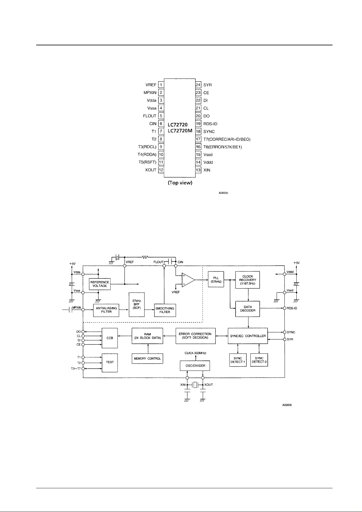
Pin Assignment
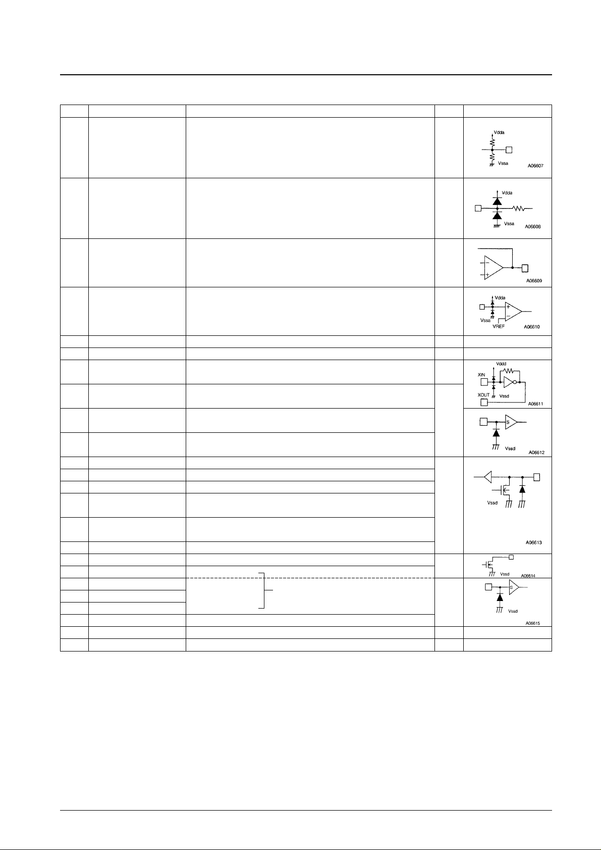
Block Diagram
No. 5602-2/14
LC72720, 72720M
Page 3
Pin Functions
No. 5602-3/14
LC72720, 72720M
Pin No. Pin name Function I/O Pin circuit
1 VREF Reference voltage output (Vdda/2) Output
2 MPXIN Baseband (multiplexed) signal input Input
5 FLOUT Subcarrier output (filter output) Output
6 CIN Subcarrier input (comparator input) Input
3 Vdda Analog system power supply (+5 V) — —
4 Vssa Analog system ground — —
12 XOUT Crystal oscillator output (4.332/8.664 MHz) Output
13 XIN Crystal oscillator input (external reference signal input)
7 T1 Test input (This pin must always be connected to ground.) Input
8 T2
Test input (standby control)
0: Normal operation, 1: Standby state (crystal oscillator stopped)
9 T3 (RDCL) Test I/O (RDS clock output)
10 T4 (RDDA) Test I/O (RDS data output)
11 T5 (RSFT) Test I/O (soft-decision control data output)
16 T6 (ERROR/57K/BE1)
Test I/O (error status output, regenerated carrier output, error block count
I/O*
output)
17 T7 (CORREC/ARI-ID/BE0)
Test I/O (Error correction status output, SK detection output, error block count
output)
18 SYNC Block synchronization detection output
19 RDS-ID RDS detection output
Output
20 DO Data output
21 CL Clock input
22 DI Data input
Input
23 CE Chip enable
24 SYR Synchronization and RAM address reset (active high)
14 Vddd Digital system power supply (+5 V) — —
15 Vssd Digital system ground — —
Note: * Normally function as an output pin. Used as an I/O pin in test mode, which is not available to user applications.
Serial data interface (CCB)
Page 4
No. 5602-4/14
LC72720, 72720M
Parameter Symbol Conditions Ratings Unit
Maximum supply voltage V
DD
max Vddd, Vdda –0.3 to +7.0 V
V
IN
1 max CL, DI, CE, SYR, T1, T2, T3, T4, T5, T6, T7, SYNC –0.3 to +7.0 V
Maximum input voltage V
IN
2 max XIN –0.3 to Vddd +0.3 V
V
IN
3 max MPXIN, CIN –0.3 to Vdda +0.3 V
V
O
1 max DO, SYNC, RDS-ID, T3, T4, T5, T6, T7 –0.3 to +7.0 V
Maximum output voltage V
O
2 max XOUT –0.3 to Vddd +0.3 V
V
O
3 max FLOUT –0.3 to Vdda +0.3 V
I
O
1 max DO, T3, T4, T5, T6, T7 6.0 mA
Maximum output current I
O
2 max XOUT, FLOUT 3.0 mA
I
O
3 max SYNC, RDS-ID 20.0 mA
Allowable power dissipation Pd max Ta ≤ 85°C
DIP24S: 350 mW
MFP24: 300 mW
Operating temperature Topr –40 to +85 °C
Storage temperature Tstg –55 to +125 °C
Specifications
Absolute Maximum Ratings at Ta = 25°C, Vssd = Vssa = 0 V
Parameter Symbol Conditions
Ratings
Unit
min typ max
Supply voltage
V
DD
1 Vddd, Vdda 4.5 5.0 5.5 V
V
DD
2 Vddd: Serial data hold voltage 2.0 V
Input high-level voltage V
IH
CL, DI, CE, SYR, T1, T2 0.7 Vddd 6.5 V
Input low-level voltage V
IL
CL, DI, CE, SYR, T1, T2 0 0.3 Vddd V
Output voltage V
O
DO, SYNC, RDS-ID, T3, T4, T5, T6, T7 6.5 V
V
IN
1 MPXIN : f = 57 ±2 kHz 50 mVrms
Input amplitude V
IN
2 MPXIN : 100% modulation composite 100 mVrms
V
XIN
XIN 400 1500 mVrms
Guaranteed crystal oscillator frequencies Xtal
XIN, XOUT : CI ≤ 120 Ω (XS = 0) 4.332 MHz
XIN, XOUT : CI ≤ 70 Ω (XS = 1) 8.664 MHz
Crystal oscillator frequency deviation TXtal XIN, XOUT : f
O
= 4.322 MHz, 8.664 MHz ±100 ppm
Data setup time t
SU
DI, CL 0.75 µs
Data hold time t
HD
DI, CL 0.75 µs
Clock low-level time t
CL
CL 0.75 µs
Clock high-level time t
CH
CL 0.75 µs
CE wait time t
EL
CE, CL 0.75 µs
CE setup time t
ES
CE, CL 0.75 µs
CE hold time t
EH
CE, CL 0.75 µs
CE high-level time t
CE
CE 20 ms
Data latch change time t
LC
1.15 µs
t
DC
DO, CL: Differs depending on the value of the
0.46 µs
Data output time
pull-up resistor used.
t
DH
DO, CE: Differs depending on the value of the
0.46 µs
pull-up resistor used.
Allowable Operating Ranges at Ta = –40 to +85°C, Vssd = Vssa = 0 V
Parameter Symbol Conditions
Ratings
Unit
min typ max
Input resistance Rmpxin MPXIN–Vssa : f = 57 kHz 23 kΩ
Internal feedback resistance Rf XIN 1.0 MΩ
Center frequency fc FLOUT 56.5 57.0 57.5 kHz
–3 dB bandwidth BW – 3 dB FLOUT 2.5 3.0 3.5 kHz
Gain Gain MPXIN–FLOOUT : f = 57 kHz 28 31 34 dB
Att1 FLOUT : ∆f = ±7 kHz 30 dB
Stop band attenuation Att2 FLOUT : f < 45 kHz, f > 70 kHz 40 dB
Att3 FLOUT : f < 20 kHz 50 dB
Electrical Characteristics at Ta = –40 to +85°C, Vssd = Vssa = 0 V
Continued on next page.
Page 5
No. 5602-5/14
LC72720, 72720M
Parameter Symbol Conditions
Ratings
Unit
min typ max
Reference voltage output Vref VREF : Vdda = 5 V 2.5 V
Hysteresis V
HIS
CL, DI, CE, SYR, T1, T2 0.1 Vddd V
Output low-level voltage
V
OL
1 DO, T3, T4, T5, T6, T7 : I = 2 mA 0.4 V
V
OL
2 SYNC, RDS-ID : I = 8 mA 0.4 V
Input high-level current
I
IH
1 CL, DI, CE, SYR, T1, T2 : VI= 6.5 V 5.0 µA
I
IH
2 XIN : VI= Vddd 2.0 11 µA
Input low-level current
I
IL
1 CL, DI, CE, SYR, T1, T2 : VI= 0 V 5.0 µA
I
IL
2 XIN : VI= 0 V 2.0 11 µA
Output off leakage current I
OFF
DO, SYNC, RDS-ID, T3, T4, T5, T6, T7 :
5.0 µA
V
O
= 6.5 V
Current drain Idd Vddd + Vdda 12 mA
Continued from preceding page.
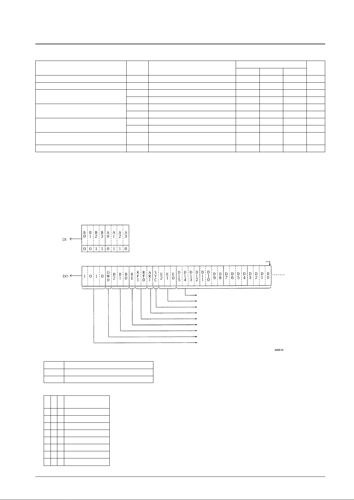
CCB Output Data Format
• Each block of output data consists of 32 bits (4 bytes), of which 2 bytes are RDS data and 2 bytes are flag data.
• Any number of 32-bit output data blocks can be output consecutively.
• When there is no data that can be read out in the internal memory, the system outputs blocks of all-zero data
consecutively.
• If data readout is interrupted, the next read operation starts with the 32-bit data block whose readout was interrupted.
However, if only the last bit remains to be read, it will not be possible to reread that whole block.
• The check bits (10 bits) are not output.
1. Offset word detection flag (1 bit): OWD
2. Offset word information flag (3 bits): B0 to B2
OWD Offset word detection
1 Detected
0 Not detected (protection function operating)
B B B
Offset word
2 1 0
0 0 0 A
0 0 1 B
0 1 0 C
0 1 1 C’
1 0 0 D
1 0 1 E
1 1 0 Unused
1 1 1 Unused
CCB address 6C
Output data/first bit
Last bit
(8) RDS data
(7) Error information flags
(6) Synchronization established flag
(5) ARI (SK) detection flag
(4) RAM data remaining flag
(3) Consecutive RAM read out possible flag
(2) Offset word information flag
(1) Offset word detection flag
Fixed pattern (1010)
Page 6

No. 5602-6/14
LC72720, 72720M
3. Consecutive RAM readout possible flag (1 bit): RE
RE RAM data information
1 The next data to be read out is in RAM.
0 This data item is the last item in RAM, and the next data is not present.
ARI SK signal
1 Detected
0 Not detected
4. RAM data remaining flag (2 bits): RF0, RF1
Caution: This value is only meaningful when RE is 1. When RE is 0, there is no data in RAM, even if RF is 00.
If a synchronization reset was applied using SYR, then the backward protection block data that was written to memory is also counted in this value.
Caution: This flag indicates the synchronization state of the circuit at the point where the data block being output was received.
On the other hand, the SYNC pin (pin 18) output indicates the current synchronization state of the circuit.
Caution: If the number of errors exceeds the value of the EC0 to EC2 setting (see the section on the CCB input format), the error information flags will be set
to the “Correction not possible” value.
RF1 RF0 Remaining data in RAM (number of blocks)
0 0 1 to 7
0 1 8 to 15
1 0 16 to 23
1 1 24
5. ARI (SK) detection flag (1 bit): ARI
SYC Synchronization detection
1 Synchronized
0 Not synchronized
6. Synchronization established flag (1 bit): SYC
7. Error information flags (3 bits): E0 to E2
8. RDS data (16 bits): D0 to D15
This data is output with the MSB first and the LSB last.
Caution: When error correction was not possible, the input data is output without change.
E E E Number of
2 1 0 bits corrected
0 0 0 0 (no errors)
0 0 1 1
0 1 0 2
0 1 1 3
1 0 0 4
1 0 1 5
1 1 0 Correction not possible
1 1 1 Unused
Page 7

CCB Input Data Format
Caution: The bits labeled with an asterisk must be set to 0.
1. Synchronization protection (forward protection) method setting (4 bits): FS0 to FS3
FS3 = 0: If offset words in the correct order could not be detected continuously during the number of blocks specified
by FS0 to FS2, take that to be a lost synchronization state.
FS3 = 1: If blocks with uncorrectable errors were received consecutively during the number of blocks specified by
FS0 to FS2, take that to be a lost synchronization state.
No. 5602-7/14
LC72720, 72720M
Initial value: FS0 = 0, FS1 = 1, FS2 = 0, FS3 = 0
Initial value: BS = 0
F F F
S S S Condition for detecting lost synchronization
0 1 2
0 0 0 If 3 consecutive blocks matching the FS3 condition are received.
1 0 0 If 4 consecutive blocks matching the FS3 condition are received.
0 1 0 If 5 consecutive blocks matching the FS3 condition are received.
1 1 0 If 6 consecutive blocks matching the FS3 condition are received.
0 0 1 If 8 consecutive blocks matching the FS3 condition are received.
1 0 1 If 10 consecutive blocks matching the FS3 condition are received.
0 1 1 If 12 consecutive blocks matching the FS3 condition are received.
1 1 1 If 16 consecutive blocks matching the FS3 condition are received.
2. Synchronization detection method setting (1 bit): BS
BS Synchronization detection conditions
0 If, during 3 blocks, 2 blocks of offset words were detected in the correct order.
1 If the offset words were detected in the correct order in 2 consecutive blocks.
[1] CCB address 6A
[2] CCB address 6B
IN1 data, first bit
IN2 data, first bit
(11) Circuit control
(5) Error correction method setting
(4) RAM write control
(3) Synchronization and RAM address reset
(2) Synchronization detection method setting
(1) Synchronization protection method setting
(10) Test mode settings
(9) Output pin settings
(8) RDS/RBDS selection
(7) Demodulation circuit phase control
(6) Crystal oscillator frequency selection
(11) Circuit control
Page 8

No. 5602-8/14
LC72720, 72720M
3. Synchronization and RAM address reset (1 bit): SYR
Initial value: SYR =0
Caution: 1. To apply a synchronization reset, set SYR to 1 temporarily using the CCB, and then set it back to 0 again using the CCB.
The circuit will start synchronization capture operation at the point SYR is set to 0.
2. The SYR pin (pin 24) also provides an identical reset control operation. Applications can use either method. However, the control method
that is not used must be set to 0 at all times. Any pulse with a width of over 250 ns will suffice.
3. A reset must be applied immediately after the reception channel is changed. If a reset is not applied, reception data from the previous
channel may remain in memory.
4. Data read out after a synchronization reset is read out starting with the backward protection block data preceding the establishment of
synchronization.
SYR Synchronization detection circuit RAM
0 Normal operation (reset cleared) Normal write (See the description of the OWE bit.)
1 Forced to the unsynchronized state (synchronization reset)
After the reset is cleared, start writing from the data prior to the
establishment of synchronization, i.e. the data in backward protection.
Initial value: OWE = 0
Initial values: EC0 = 0, EC1 = 1, EC2 = 0, EC3 = 0, EC4 = 1
Caution: 1. If soft-decision A or soft-decision B is specified, soft-decision control will be performed even if the number of bits corrected is set to 0 (error
detection only). With these settings, data will be output for blocks with no errors.
2.As opposed to soft-decision B, the soft-decision A setting suppresses soft decision error correction.
4. RAM write control (1 bit): OWE
5. Error correction method setting (5 bits): EC0 to EC4
OWE RAM write conditions
0 Only data for which synchronization had been established is written.
1 Data for which synchronization not has been established (unsynchronized data) is also written. (However, this applies when SYR = 0.)
E E E
Number of
C C C
bits corrected
0 1 2
0 0 0 0 (error detection only)
1 0 0 1 or fewer bits
0 1 0 2 or fewer bits
1 1 0 3 or fewer bits
0 0 1 4 or fewer bits
1 0 1 5 or fewer bits
0 1 1 Illegal value
1 1 1 Illegal value
E E
C C Soft-decision setting
3 4
0 0 Mode 0: Hard decision
1 0 Mode 1: Soft decision A
0 1 Mode 2: Soft decision B
1 1 Illegal value
6. Crystal oscillator frequency selection (1 bit): XS
XS = 0: 4.332 MHz
XS = 1: 8.664 MHz
Initial value: XS = 0
7. Demodulation circuit phase control (2 bits): PL0, PL1
Initial values: PL0 = 0, PL1 = 1
Caution: 1. When PL0 is 0 (normal operation), the LSI detects the presence or absence of the ARI signal and reproduces the RDS data by automatically
controlling the demodulation phase with respect to the reproduced carrier. However, the initial phase following a synchronization reset is set
by PL1.
2.If PL0 is set to 1, the demodulation circuit phase is locked according to the PL1 setting at either 90° (PL1 = 0) or 0° (PL1 = 1), allowing RDS
data to be reproduced. When ARI is not present, PL1 should be set to 0, since the RDS data is reproduced by detecting at a phase of 90°
with respect to the reproduced carrier. When ARI is present, PL1 should be set to 1, since detection is at 0°. In cases where the ARI
presence is known in advance, more stable reproduction can be achieved by fixing the demodulation phase in this manner.
PL0 PL1 Demodulation circuit phase control
0 0/1 <Normal operation> when ARI presence or absence is unclear.
1
0 If the circuit determines that the ARI signal is absent: 90° phase
1 If the circuit determines that the ARI signal is present: 0° phase
Page 9

No. 5602-9/14
LC72720, 72720M
8. RDS/RBDS (MMBS) selection (1 bit): RM
Initial value: RM = 0
—: Open, ●●, ●: Output enabled (● = reverse polarity)
Initial values: PT0 = 1, PT1 = 1, PT2 = 0 (mode 3)
Caution: 1. When PT2 is set to 1, the polarity of the T3 (RDCL), T6 (ERROR/57K), T7 (CORREC/ARI-ID) SYNC, and RDS-ID pins changes to active
high.
2.The output pins (T3 to T7, SYNC, and RDS-ID) are all open-drain pins, and require external pull-up resistors to output data.
These pins indicate the number of blocks in a set of 48 blocks that had errors before correction. The output polarity of these pins is fixed at the values
listed in the table.
RM RBDS support Decoding method
0 None Only RDS data is decoded correctly (Offset word E is not detected.)
1 Provided RDS and MMBS data is decoded correctly (Offset word E is also detected.)
9. Output pin settings (3 bits): PT0 to PT2
These bits control the T3, T4, T5, T6, T7, SYNC, and RDS-ID pins.
P P P
T3 T4 T5 T6 T7
Mode T T T
0 1 2 RDCL RDDA RSFT ERROR 57K BE1 CORREC ARI-ID BE0
0 0 0 0 — — — — — — — — —
1 1 0 0 ●● ●● ●● — — — — — —
2 0 1 0 ●● ●● ●● — ●● — — ●● —
3 1 1 0 ●● ●● ●● ●● — — ●● — —
4 0 0 1 — — — — — ●● — — ●●
5 1 0 1 ● ●● ●● — — — — — —
6 0 1 1 ● ●● ●● — ● — — ● —
7 1 1 1 ● ●● ●● ● — — ● — —
Pin T3 (RDCL)
PT2 = 0 Data (RDDA and RSFT) changes on this pin’s rising edge.
PT2 = 1 Data (RDDA and RSFT) changes on this pin’s falling edge.
Mode 2 (PT2 = 0) Pin T7 (ARI-ID)
No SK High (1)
SK present Low (0)
Mode 3 (PT2 = 0) Pin T6 (ERROR) Pin T7 (CORREC)
Correction not possible Low (0) Low (0)
Errors corrected High (1) Low (0)
No errors High (1) High (1)
Mode 4
Pin T6 (BE1) Pin T7 (BE0)
Number of error blocks (B)
B = 0 Low (0) Low (0)
1 ≤ B ≤ 20 Low (0) High (1)
20 < B ≤ 40 High (1) Low (0)
40 < B ≤ 48 High (1) High (1)
Page 10

No. 5602-10/14
LC72720, 72720M
Caution: The output indicates the synchronization state for the previous block.
Mode (PT2 = 0) The SYNC pin
0 to 2 When synchronized: Low (0). When unsynchronized: High (1)
When synchronized: Goes high for a fixed period (421 µs) at
3 the start of a block and then goes low.
When unsynchronized: High (1)
When PT2 = 0 The RDS-ID pin
No RDS High (1)
RDS present Low (0)
10. Test mode settings (4 bits): TS0 to TS3
Initial values: TS0 = 0, TS1 = 0, TS2 = 0, TS3 = 0
(Applications must set these bits to the above values.)
Notes: The T1 and T2 pins (pins 7 and 8) are related to test mode as follows:
The T1 pin must be tied to VSS(0 V).
Initial values: CT0 = 0, CT1 = 0
Pin T1 Pin T2 LSI operation Notes
0 0 Normal operating mode
These states are user settable
0 1 Standby mode (crystal oscillator stopped)
1 0/1 LSI test mode Users cannot use this state
11. Circuit control (2 bits): CT0 and CT1
RDCL/RDDA/RSFT and ERROR/CORREC/SYNC Output Timing
Timing 1 (modes 1 to 3, PT2 = 0)
Timing 2 (mode 3, PT2 = 0)
Item Control
CT0 RSFT control When set to 1, soft-decision control data (RSFT) is easier to generate.
CT1 RDS-ID detection condition When set to 1, the RDS-ID detection conditions are made more restrictive.
RDCL output
RDDA output
RSFT output
Input data
Error crrection
SYNC output
ERROR output
CORREC output
Sync NG
Sync NGSync NG
Sync OK
Sync OKSync OK
Sync OK Sync OK
Data
corrected
Data
corrected
No
errors
No
errors
Uncorrectable
Uncorrectable
Note: When PT2 = 0, RDDA and RSFT must be
aquired on the falling edge of RDCL.
Page 11

Serial Data Input and Output Methods
Data is input and output using the CCB (computer control bus), which is the Sanyo audio LSI serial bus format. This LSI
adopts an 8-bit address CCB format.
Serial data input (IN1, IN2) tSU, tHD, tEL, tES, tEH≥ 0.75 µs tLC< 1.15µs tCE< 20 ms
CL: Normal high
CL: Normal low
Caution: The serial data I/O function can access data only after the crystal oscillator circuit is operating.
No. 5602-11/14
LC72720, 72720M
I/O mode
(LSB) Address (MSB)
Comment
B0 B1 B2 B3 A0 A1 A2 A3
1 IN1 (6A) 0 1 0 1 0 1 1 0
· Control data input mode, also referred to as “serial data input” mode.
· This is a 16-bit data input mode.
2 IN2 (6B) 1 1 0 1 0 1 1 0
· Control data input mode, also referred to as “serial data input” mode.
· This is a 16-bit data input mode.
3 OUT (6C) 0 0 1 1 0 1 1 0
· Data output mode, also referred to as “serial data output” mode.
· The data for multiple blocks can be output sequentially in this mode.
I/O mode determined
For the CL normal high state
For the CL normal low state
Internal data
Internal data
Page 12

No. 5602-12/14
LC72720, 72720M
Serial data output (OUT) tSU, tHD, tEL, tES, tEH≥ 0.75 µs tDC, tDH< 0.46 µs tCE< 20 ms
CL: Normal high
CL: Normal low
Serial data timing
CL: Normal high
CL: Normal low
Caution:1. Since the DO pin is an n-channel open-drain output, the transition times (tDC, tDH) will differ with the value
of the pull-up resistor used.
2. The CE, CL, DI, and DO pins can be connected to the corresponding pins on other LSIs that use the CCB
interface. (However, we recommend connecting the DO and CE pins separately if the number of available
microcontroller ports allows it.)
DO
Intenal data latch
Intenal data latch
Old
Old
New
New
Page 13

Parameter Symbol Conditions
Ratings
Unit
min typ max
Data setup time t
SU
DI, CL 0.75 µs
Data hold time t
HD
DI, CL 0.75 µs
Clock low-level time t
CL
CL 0.75 µs
Clock high-level time t
CH
CL 0.75 µs
CE wait time t
EL
CE, CL 0.75 µs
CE setup time t
ES
CE, CL 0.75 µs
CE hold time t
EH
CE, CL 0.75 µs
CE high-level time t
CE
CE 20 ms
Data latch transition time t
LC
1.15 µs
Data output time
t
DC
DO, CL 0.46 µs
t
DH
DO, CE 0.46 µs
No. 5602-13/14
LC72720, 72720M
Differs with the value of
the pull-up resistor used.
DO pin operation
This LSI incorporates a RAM data buffer that can hold up to 24 blocks of data. At the point where one block of data is
written to this RAM, the LSI issues a read request by switching the DO pin from high to low.
The DO pin always goes high for a fixed period (Tdo = 265 µs) after a readout and CE goes low. When all the data in the
data buffer has been read out, the DO pin is held in the high state until a new block of data has been written to the RAM. If
there is data that has not yet been read remaining in the data buffer, the DO pin goes low after the Tdo time has elapsed.
After a synchronization reset, the DO pin is held high until synchronization is established. It goes low at the point where
the LSI synchronizes.
1. When the DO pin is high following the 265 µs period (Tdo) after data is read out
Here, the buffer is in the empty state, i.e. the state where new data has not been written. After this, when the DO pin
goes low, applications are guaranteed to be able to read out that data without it being overwritten by new data if they
start a readout operation within 480 ms of DO going low.
2. When DO goes low 265 µs after data is read out
Here, there is data that has not been read out remaining in the data buffer. In this case, applications are guaranteed to
be able to read out that data without it being overwritten by new data if they start a readout operation within 20 ms of
DO going low. (Note that this is the worst case condition.)
Notes: 1. Although an application can determine whether or not there is data remaining in the buffer by checking the DO
level with the above timing, checking the RE and RF flags in the serial data is a preferable method.
2. Applications are not limited to reading out one block of data at a time, but rather can read out multiple blocks
of data continuously as described above. When using this method, if an application references the RE and RF
flags in the data while reading out data, it can determine the amount of data remaining. However, the length of
the period for data readout (the period the CE pin remains high) must be kept under 20 ms.
3. If the DO pin is shared with other LSIs that use the CCB interface, the application must identify which LSI
issued the readout request. One method is to read out data from the LC72720 and either check whether
meaningful data has been read (if the LC72720 is not requesting a read, data consisting of all zeros will be read
out) or check whether the DO level goes low within the 256 µs following the completion of the read (if the DO
pin goes low, then the request was from another LSI).
CE pin
DO pin
CE pin
DO pin
(Last data) - 1
Last data
New data
(Last data) - 2 (Last data) - 1
Last data
DO check (Tdo < T)
DO check (Tdo < T)
Page 14

No. 5602-14/14
LC72720, 72720M
This catalog provides information as of May, 1997. Specifications and information herein are subject to change
without notice.
■ No products described or contained herein are intended for use in surgical implants, life-support systems, aerospace
equipment, nuclear power control systems, vehicles, disaster/crime-prevention equipment and the like, the failure of
which may directly or indirectly cause injury, death or property loss.
■ Anyone purchasing any products described or contained herein for an above-mentioned use shall:
➀
Accept full responsibility and indemnify and defend SANYO ELECTRIC CO., LTD., its affiliates, subsidiaries and
distributors and all their officers and employees, jointly and severally, against any and all claims and litigation and all
damages, cost and expenses associated with such use:
➁
Not impose any responsibility for any fault or negligence which may be cited in any such claim or litigation on
SANYO ELECTRIC CO., LTD., its affiliates, subsidiaries and distributors or any of their officers and employees
jointly or severally.
■ Information (including circuit diagrams and circuit parameters) herein is for example only; it is not guaranteed for
volume production. SANYO believes information herein is accurate and reliable, but no guarantees are made or implied
regarding its use or any infringements of intellectual property rights or other rights of third parties.
Sample Application Circuit
Notes: 1. Determine the value of the DO pin pull-up resistor based on the required serial data transfer speed.
2. A 100-kΩ bias resistor must be connected between the CIN pin and the VREF pin. Note that this resistor is planned to be included internally to the
LSI in later versions of this product.
3. If the SYR pin is unused, it must be connected to ground.
 Loading...