

Page 1

Ordering number : ENN6167
12100RM (OT) No. 6167-1/29
Overview
The LC72711W and LC72711LW are data demodulator
ICs for receiving FM multiplex broadcasts for mobile
reception in the DARC format. This IC includes an onchip bandpass filter for extracting the DARC signal from
the FM baseband signal. Furthermore, since this IC
supports all of the IT-R recommended FM multiplex
frame structures (methods A, A', B, and C), it is optimal
for worldwide market radios that provide FM multiplex
reception. The LC72711W and LC72711LW support both
parallel and CCB serial CPU interfaces.
Functions
• Adjustment-free 76 kHz SCF bandpass filter
• Supports all FM multiplex frame structures (methods A,
A', B, and C) under CPU control.
• MSK delay detection system based on a 1T delay.
• Error correction function based on a 2T delay (in the
MSK detection stage)
• Digital PLL based clock regeneration function
• Shift-register 1T and 2T delay circuits
• Block and frame synchronization detection circuits
• Functions for setting the number of allowable BIC errors
and the number of synchronization protection
operations.
• Error correction using (272, 190) codes
• Built-in layer 4 CRC code checking circuit
• On-chip frame memory and memory control circuit for
vertical correction
• 7.2 MHz crystal oscillator circuit
• Two power saving modes: STNBY and EC_STOP
• Applications can use either a parallel CPU interface
(DMA) or a CCB serial interface.
• Supply voltage: 4.5 to 5.5 V (LC72711W), 2.7 to 3.6 V
(LC72711LW)
Package Dimensions
unit: mm
3190-SQFP64
10.0
12.0
1.25
0.51.25
1.25 0.5 1.250.18
12.0
116
17
32
33
48
49
64
10.0
0.5
1.7max
0.5
0.1
0.15
SANYO: SQFP64
[LC72711W, 72711LW]
LC72711W, 72711LW
SANYO Electric Co.,Ltd. Semiconductor Company
TOKYO OFFICE Tokyo Bldg., 1-10, 1 Chome, Ueno, Taito-ku, TOKYO, 110-8534 JAPAN
Mobile FM Multiplex Broadcast (DARC)
Receiver IC
CMOS IC
Any and all SANYO products described or contained herein do not have specifications that can handle
applications that require extremely high levels of reliability, such as life-support systems, aircraft’s
control systems, or other applications whose failure can be reasonably expected to result in serious
physical and/or material damage. Consult with your SANYO representative nearest you before using
any SANYO products described or contained herein in such applications.
SANYO assumes no responsibility for equipment failures that result from using products at values that
exceed, even momentarily, rated values (such as maximum ratings, operating condition ranges, or other
parameters) listed in products specifications of any and all SANYO products described or contained
herein.
• CCB is a trademark of SANYO ELECTRIC CO., LTD.
• CCB is SANYO’s original bus format and all the bus
addresses are controlled by SANYO.
Page 2
No. 6167-2/29
LC72711W, 72711LW
Parameter Symbol Conditions Ratings Unit
Maximum supply voltage V
DD
(–0.3 to +5.5) –0.3 to +7.0 V
Input voltage
V
IN
(1) A0/CL, A1/CE, A2/DI, RST, STNBY –0.3 to +7.0 V
V
IN
(2) Pins other than VIN(1) –0.3 to VDD+ 0.3 V
Output voltage
V
OUT
(1) DO –0.3 to +7.0 V
V
OUT
(2) Pins other than V
OUT
(1) –0.3 to VDD+ 0.3 V
Output current
I
OUT
(1) INT, RDY, DREQ, and D0 to D15 0 to 4.0 mA
I
OUT
(2) Pins other than I
OUT
(1) 0 to 2.0 mA
Allowable output current (total) I
TTL
Total for all the output pins 20 mA
Allowable power dissipation Pdmax Ta ≤ +85°C 200 mW
Operating temperature Topr –40 to +85 °C
Storage temperature Tstg –55 to +125 °C
Specifications
Absolute Maximum Ratings at Ta = +25°C, VSS= 0 V. Items in parentheses refer to the LC72711LW.
Parameter Symbol Conditions
Ratings
Unit
min typ max
Supply voltage V
DD
4.5 5.5 V
High-level input voltage
V
IH
1 A0/CL, A1/CE, A2/DI, RST, STNBY 0.7 V
DD
5.5 V
V
IH
2 DACK, WR, RD, CS, SP, BUSWD, A3, IOCNT1, IOCNT2 0.7 V
DD
V
DD
V
Low-level input voltage
V
IL
1 Pins for which VIH1 applies V
SS
0.3 V
DD
V
V
IL
2 Pins for which VIH2 applies V
SS
0.3 V
DD
V
Oscillator frequency FOSC This IC operates with a frequency precision of ±250 ppm 7.2 MHz
X
IN
input sensitivity VXI
With a sine wave input to X
IN
, capacitor coupling,
400 1500 mVrms
V
DD
= +4.5 to +5.5 V
Input amplitude VMPX
With a 100% modulated composite signal input to
150 400 mVrms
MP
XIN
, VDD= +4.5 to +5.5 V
Clock low-level period t
CL
A0/CL 0.7 µs
Clock high-level period t
CH
A0/CL 0.7 µs
Data setup time t
SU
A0/CL, A2/DI 0.7 µs
Data hold time t
HD
A0/CL, A2/DI 0.7 µs
CE wait time t
EL
A0/CL, A1/CE 0.7 µs
CE setup time t
ES
A0/CL, A1/CE 0.7 µs
CE hold time t
EH
A0/CL, A1/CE 0.7 µs
Data latch change time t
LC
A1/CE 0.7 µs
Data output time t
DDO
DO, A0/CL 277 555 ns
CRC4 change time t
CRC
CRC4, A0/CL 0.7 µs
[LC72711W]
Allowable Operating Ranges at Ta = –40 to +85°C, VSS= 0 V
Serial I/O
Page 3

No. 6167-3/29
LC72711W, 72711LW
[LC72711W]
Allowable Operating Ranges: Parallel Interface at Ta = –40 to +85°C, VSS= 0 V
Notes: Application designs must take the RDY signal output delay into consideration if the RDY signal is used as the CPU bus wait signal.
When the RDY signal is used, the “RD low-level width” and the “Corrected output RD width” values express the basic timing (excluding the wait
time) settings for the CPU bus.
If the RDY signal is not used, (that is, if no wait states are inserted) the value of the RD low-level width will be 250 ns (minimum).
Parameter Symbol Conditions
Ratings
Unit
min typ max
Address to RD setup t
SARD
A0/CL, A1/CE, A2/DI, A3, RD 20 ns
RD to address hold t
HARD
A0/CL, A1/CE, A2/DI, A3, RD, t
WRDL
→250 ns –20 ns
RD low-level width t
WRDL
1 RD 250 ns
RD low-level width (when RDY is used) t
WRDL
2 RD 100 250 ns
RD cycle wait t
CYRD
A0/CL, A1/CE, A2/DI, A3, RD 150 ns
RDY width (Register read) t
WRDY
RDY 60 210 ns
RD data hold t
RDH
RD, DATn 0 ns
Address to WR setup t
SAWR
A0/CL, A1/CE, A2/DI, A3, WR 20 ns
WR to address hold t
HAWR
A0/CL, A1/CE, A2/DI, A3, WR 20 ns
WR cycle wait t
CYWR
A0/CL, A1/CE, A2/DI, A3, WR 150 ns
WR low-level width t
WWRL
WR 200 ns
WR data hold t
WDH
WR, DATn 0 ns
RDY output delay t
DRDY
RD, RDY 0 30 ns
Corrected output RD width t
WDRD
1
RD (BUSWD = L 8 bits) 300 ns
RD (BUSWD = H 16 bits) 540 ns
Corrected output RD width
t
WDRD
2
RD (BUSWD = L 8 bits) 100 300 ns
(when RDY is used) RD (BUSWD = H 16 bits) 300 540 ns
RDY width (corrected output read) t
WDRDY
RDY (BUSWD = L 8 bits) 60 210 ns
RDY ((BUSWD = H 16 bits) 300 490 ns
DACK to DREQ delay t
DREQ
DREQ, DACK 260 ns
DMA cycle wait t
CYDM
RD, DREQ 420 ns
RD low-level width (DMA) t
WRDM
RD 300 ns
Parallel I/O
Page 4

No. 6167-4/29
LC72711W, 72711LW
Parameter Symbol Conditions
Ratings
Unit
min typ max
Supply voltage V
DD
2.7 3.6 V
High-level input voltage
V
IH
1 A0/CL, A1/CE, A2/DI, RST, STNBY 0.7 V
DD
5.5 V
V
IH
2 DACK, WR, RD, CS, SP, BUSWD, A3, IOCNT1, IOCNT2 0.7 V
DD
V
DD
V
Low-level input voltage
V
IL
1 Pins for which VIH1 applies V
SS
0.3 V
DD
V
V
IL
2 Pins for which VIH2 applies V
SS
0.3 V
DD
V
Oscillator frequency FOSC This IC operates with a frequency precision of ±250 ppm 7.2 MHz
X
IN
input sensitivity VXI
With a sine wave input to X
IN
, capacitor coupling.
400 900 mVrms
V
DD
= +2.7 to +3.6 V
VMPX1
With a 100% modulated composite signal input to
120 350 mVrms
Input amplitude
MP
XIN
. VDD= +3.3 V
VMPX2
With a 100% modulated composite signal input
120 180 mVrms
to MP
XIN
. VDD= +2.7 V
Clock low-level period t
CL
A0/CL 0.7 µs
Clock high-level period t
CH
A0/CL 0.7 µs
Data setup time t
SU
A0/CL, A2/DI 0.7 µs
Data hold time t
HD
A0/CL, A2/DI 0.7 µs
CE wait time t
EL
A0/CL, A1/CE 0.7 µs
CE setup time t
ES
A0/CL, A1/CE 0.7 µs
CE hold time t
EH
A0/CL, A1/CE 0.7 µs
Data latch change time t
LC
A1/CE 0.7 µs
Data output time t
DDO
DO, A0/CL 277 555 ns
CRC4 change time t
CRC
CRC4, A0/CL 0.7 µs
[LC72711LW]
Allowable Operating Ranges at Ta = –40 to +85°C, VSS= 0 V
Serial I/O
Page 5
No. 6167-5/29
LC72711W, 72711LW
[LC72711LW]
Allowable Operating Ranges: Parallel Interface at Ta = –40 to +85°C, VSS= 0 V
Notes: Application designs must take the RDY signal output delay into consideration if the RDY signal is used as the CPU bus wait signal.
When the RDY signal is used, the “RD low-level width” and the “Corrected output RD width” values express the basic timing (excluding the wait
time) settings for the CPU bus.
If the RDY signal is not used, (that is, if no wait states are inserted) the value of the “RD low-level width” will be 280 ns (minimum).
Parameter Symbol Conditions
Ratings
Unit
min typ max
Address to RD setup t
SARD
A0/CL, A1/CE, A2/DI, A3, RD 20 ns
RD to address hold t
HARD
A0/CL, A1/CE, A2/DI, A3, RD, t
WRDL
→250 ns –20 ns
RD low-level width t
WRDL
1 RD 280 ns
RD low-level width (when RDY is used) t
WRDL
2 RD 100 280 ns
RD cycle wait t
CYRD
A0/CL, A1/CE, A2/DI, A3, RD 150 ns
RDY width (Register read) t
WRDY
RDY 60 230 ns
RD data hold t
RDH
RD, DATn 0 ns
Address to WR setup t
SAWR
A0/CL, A1/CE, A2/DI, A3, WR 20 ns
WR to address hold t
HAWR
A0/CL, A1/CE, A2/DI, A3, WR 20 ns
WR cycle wait t
CYWR
A0/CL, A1/CE, A2/DI, A3, WR 150 ns
WR low-level width t
WWRL
WR 200 ns
WR data hold t
WDH
WR, DATn 0 ns
RDY output delay t
DRDY
RD, RDY 0 50 ns
Corrected output RD width t
WDRD
1
RD (BUSWD = L 8 bits) 300 ns
RD (BUSWD = H 16 bits) 540 ns
Corrected output RD width
t
WDRD
2
RD (BUSWD = L 8 bits) 100 300 ns
(when RDY is used) RD (BUSWD = H 16 bits) 300 540 ns
RDY width (corrected output read) t
WDRDY
RDY (BUSWD = L 8 bits) 60 230 ns
RDY ((BUSWD = H 16 bits) 300 490 ns
DACK to DREQ delay t
DREQ
DREQ, DACK 260 ns
DMA cycle wait t
CYDM
RD, DREQ 420 ns
RD low-level width (DMA) t
WRDM
RD 300 ns
Parallel I/O
Page 6

No. 6167-6/29
LC72711W, 72711LW
[LC72711W]
Electrical Characteristics at VDD= +4.5 to +5.5 V, within the allowable operating ranges
Parameter Symbol Conditions
Ratings
Unit
min typ max
V
OH
1
Io = 2 mA, BCK, FCK, BLOCK, FLOCK,
VDD– 0.4 V
High-level output voltage
CRC4, CLK16DATA
V
OH
2 Io = 4 mA, INT, RDY, DREQ, D0 to D15 VDD– 0.4 V
V
OL
1 Io = 2 mA, Pins for which VOH1 applies 0.4 V
Low-level output voltage V
OL
2 Io = 4 mA, Pins for which VOH2 applies 0.4 V
V
OL
3 Io = 2 mA, DO, INT 0.4 V
V
IH
1
V
IN
= 5.5 V, A0/CL, A1/CE, A2/DI, RST,
1.0 µA
High-level input current
STNBY
V
IH
2VIN= V
DDD
, All input pins other than IIH1 1.0 µA
Low-level input current I
IL
VIN= V
SSD
, All input pins –1.0 µA
Input resistance Rmpx MP
XIN
– Vssa f = 100 kHz 50 kΩ
Reference supply voltage output Vref Vref, Vdda = 5 V 2.5 V
Bandpass filter center frequency Fc FLOUT 76.0 kHz
–3 dB bandwidth Fbw FLOUT 19.0 kHz
Group delay Dgd FLOUT –7.5 +7.5 µs
Gain Gain FLOUT – MPXIN f = 76 kHz 20 dB
ATT1 FLOUT f = 50 kHz 25 dB
Stop band attenuation
ATT2 FLOUT f = 100 kHz 15 dB
ATT3 FLOUT f = 30 kHz 50 dB
ATT4 FLOUT f = 150 kHz 50 dB
Output off leakage current IOFF V0 = V
DDD
, DO 5.0 µA
Hysteresis voltage VHIS
A0/CL, A1/CE, A2/DI, A3, CS, RD, WR,
0.1 V
DDD
V
DACK, IOCNT1, IOCNT2, RST, STNBY
Internal feedback resistor Rf XIN, XOUT 1.0 MΩ
Current drain I
DD
18 25 mA
Page 7

No. 6167-7/29
LC72711W, 72711LW
[LC72711LW]
Electrical Characteristics at VDD= +2.7 to +3.6 V, within the allowable operating ranges
Parameter Symbol Conditions
Ratings
Unit
min typ max
V
OH
1
Io = 1 mA, BCK, FCK, BLOCK, FLOCK,
VDD– 0.4 V
High-level output voltage
CRC4, CLK16DATA
V
OH
2 Io = 2 mA, INT, RDY, DREQ, D0 to D15 VDD– 0.4 V
V
OL
1 Io = 1 mA, Pins for which VOH1 applies 0.4 V
Low-level output voltage V
OL
2 Io = 2 mA, Pins for which VOH2 applies 0.4 V
V
OL
3 Io = 1 mA, DO, INT 0.4 V
I
IH
1
V
IN
= 5.5 V, A0/CL, A1/CE, A2/DI, RST,
1.0 µA
High-level input current
STNBY
I
IH
2VIN= V
DDD
, All input pins other than IIH1 1.0 µA
Low-level input current I
IL
VIN= V
SSD
, All input pins –1.0 µA
Input resistance Rmpx MP
XIN
– Vssa f = 100 kHz 50 kΩ
Reference supply voltage output Vref Vref, Vdda = 3 V 1.5 V
Bandpass filter center frequency Fc FLOUT 76.0 kHz
–3 dB bandwidth Fbw FLOUT 19.0 kHz
Group delay Dgd FLOUT –7.5 +7.5 µs
Gain Gain FLOUT – MPXIN f = 76 kHz 20 dB
ATT1 FLOUT f = 50 kHz 25 dB
Stop band attenuation
ATT2 FLOUT f = 100 kHz 15 dB
ATT3 FLOUT f = 30 kHz 50 dB
ATT4 FLOUT f = 150 kHz 50 dB
Output off leakage current IOFF V0 = V
DDD
, DO 1.0 µA
Hysteresis voltage VHIS
A0/CL, A1/CE, A2/DI, A3, CS, RD, WR,
0.1 V
DDD
V
DACK, IOCNT1, IOCNT2, RST, STNBY
Internal feedback resistor Rf XIN, XOUT 1.0 MΩ
Current drain I
DD
12 20 mA
Page 8
Block Diagram
No. 6167-8/29
LC72711W, 72711LW
PN decoding
Memory array
LPF
MPXIN
7.2 MHz
XIN
Vssa
Vdda
XOUT
RST
CLK16
DATA
BCK
FCK
FLOCK
BLOCK
Data
Address
STNBY
Vssd
Vddd
LPF
Error correction:
layer 2 CRC
76 kHz
-BPF
(SCF)
Anti-aliasing
filter
Timing
control
Vref
Synchronization
regeneration
MSK correction
circuit
Clock
regeneration
2T delay
1T delay
IOCNT1
DACK
DREQ
IOCNT2
CRC4
FLOUT
CIN
VREF
CS
RD
WR
RDY
INT
BUSWD
TIN
SP
A3
DO
A2/DI
A1/CE
A0/CL
D0 to D15
Output control (CPU interface) and
layer 4 CRC detection circuit
Pin Assignment
IOCNT1
WR
RD
A0/CL
A1/CE
A2/DI
A3
CS
STNBY
BUSWD
SP
RST
D15
D14
NC
D13
TIN
Vssa
D12
Vref
MPXIN
D11
D10
Vdda
D9
FLOUT
D8
CIN
D7
NC
D6
TPC1
SQFP-64
(Top view)
LC72711W
LC72711LW
64
D5
TPC2
BCK
CRC4
FCK
BLOCK
FLOCK
DATA
CLK16
IOCNT2
Vddd
XOUT
INT
Vddd
Vssd
DO
NC
TEST
TOSEL1
TOSEL2
Vssd
XIN
Vddd
RDY
Vssd
DACK
DREQ
D4
D3
D2
D1
D0
Vref
49
1
32
16
Page 9

No. 6167-9/29
LC72711W, 72711LW
Pin Functions
Pin No. Pin Function I/O Pin circuit
Data bus I/O control 1 (SP = low)*
1
Data bus I/O control 2 (SP = low)*
1
DMA acknowledge (SP = low)*
1
Write control signal (SP = low)*
1
Read control signal (SP = low)*
1
Address input 0 (SP = low) CCB CL input (SP = high)
1 (SP = low) CCB CE input (SP = high)
2 (SP = low) CCB DI input (SP = high)
3 (SP = low)*
1
Chip select input (SP = L)*
1
System reset input (negative logic)
Standby mode (positive logic)
3
4
13
38
39
40
41
42
43
44
46
45
IOCNT1
IOCNT2
DACK
WR
RD
A0/CL
A1/CE
A2/DI
A3
CS
RST
STNBY
SP = low: parallel, SP = high: serial
BUSWD = low: 8 bits, BUSWD = high: 16 bits
The test pin must be connected to the digital system ground (V
SS
).
Must be connected to the digital system power supply (V
DD
) or ground
(VSS) in normal operation.
As above
As above
As above
As above
47
48
60
58
59
61
62
49
SP
BUSWD
TEST
TPC1
TPC2
TOSEL1
TOSEL2
TIN
Clock regeneration monitor
Demodulated data monitor
5
6
CLK16
DATA
Frame start signal output
Block start signal output
Outputs a high level when in frame synchronization
Outputs a high level when in block synchronization
Level 4 CRC detection result output
9
10
7
8
11
FCK
BCK
FLOCK
BLOCK
CRC4
External CPU interrupt request output
DMA request signal
Read ready signal
Input
Input
Output
I/O
33
12
16
INT
DREQ
RDY
Data bus
The bus width can be set to be either 8 bits or 16 bits by the BUSWD
pin (pin 48).
For data input, only the lower 8 bits (D0 to D7) are valid.
17 to 24 D0 to D7
Output
Data bus (in 16-bit mode)
These pins are held in the output off state when BUSWD is low.
25 to 32 D8 to D15
I/O
Connections for the system clock crystal oscillator circuit.
The XIN pin can also be used as an external clock signal input.
64
1
XIN
XOUT
InputBaseband (multiplex) signal input53 MPXIN
OutputSubcarrier output (76 kHz bandpass filter output)55 FLOUT
Continued on next page.
Page 10

No. 6167-10/29
LC72711W, 72711LW
Continued from preceding page.
Pin No. Pin Function I/O Pin circuit
Subcarrier input (comparator input)56 CIN
Vref
Input
Reference voltage output (Vdda/2)52 VREF
Vssa
Vdda
Output
CCB serial interface data output36 DO
Output
—
—
—
—
This pin must be left open
37
50
57
NC
Analog system power supply
Analog system ground
Digital system power supply (+2.7 to +5.5 V)
Digital system ground
54
51
2, 15, 34
14, 35, 63
V
DDA
V
SSA
V
DDD
V
SSD
Notes: 1. This pin must be connected to V
DDD
or V
SSD
if the IC is used in serial interface mode (when SP is high).
2. A capacitor of at least 2000 pF must be inserted between V
DDD
and V
SSD
.
Page 11

Control Registers
This IC includes both registers that can be read and registers that can be written. These registers can be accessed using
either the serial interface (CCB) or the parallel interface. The SP pin switches between these interfaces.
The initial values of the write registers are the data loaded into internal registers when a reset signal (RST) is received.
These values are recommended values that do not need to be changed during normal operation.
If the parallel interface is used, applications must hold the address fixed at 00H when reading out data to which error
correction has been applied. If the CCB interface is used, the application needs only to specify the CCB address (#FB).
The address 00H is an invalid address for writing.
The addresses other than those specified below are control addresses particular to the IC. Applications must not specify
those addresses.
The synchronization circuit in this IC operates by recognizing a 16-bit BIC code. The number of allowable errors is the
number of incorrect bits allowed in those 16 bits. This data sets up separate values for forward protection mode (when
synchronized) and for back protection mode (when not synchronized).
The default value is to allow 2 incorrect bits in both forward and back modes. If the block synchronization discrimination
output (BLOCK) is used for discriminating whether or not FM multiplex data is present, we recommend setting the back
protection mode BIC allowable error count to 1 or 0.
No. 6167-11/29
LC72711W, 72711LW
Address Register Function R/W Address Register Function R/W
1 BIC Number of allowable BIC errors W 1 STAT Status register R
2 SYNCB Block synchronization: error protection count W 2 BLNO Block number register R
3 SYNCF Frame synchronization: error protection count W
4 CTL1 Control register 1 W
5 CTL2 Control register 2 W
6 CRC4 Layer 4 CRC register W
Number of Allowable BIC Errors
Address Register R/W Initial value BIT7 BIT6 BIT5 BIT4 BIT3 BIT2 BIT1 BIT0
01H BIC W 22H Back protection (LSB) Forward protection (LSB)
The synchronization protection count can be set separately for both forward and back protection. The count conditions
for the protection counts are as follows.
• Back protection mode (not synchronized: BLOCK = low)
If the timing of the IC internal synchronization free-running counter matches the timing of the received BIC, the
protection count is incremented by 1. Contrarily, if the timings of the IC internal counter and the received BIC do not
match, the protection counter is cleared to 0. The timing of the count is the timing of the IC internal counter.
• Forward protection mode (synchronized: BLOCK = high)
In reverse to the back protection mode, if the timing of the IC internal free-running counter does not match the
detection timing of the received BIC, the protection counter is incremented, and if the timings match, the protection
counter is cleared to 0.
Figure 1 shows the states of the protection counter for the cases where the forward and back protection counts are both 3.
This IC defines the value of the protection counter to be 1 at the point that a match or a discrepancy between the IC
internal timing and the timing of the received BIC occurs. For example, when the value of the back protection count is 2,
the IC internal timing and the timing of the received BIC will have matched two times consecutively.
If the protection data is set to new values, for example if the protection counts are set to 3 as assumed in figure 1,
applications must send values which are 1 less than the intended value; in this case 22H. Similarly, if the value is set to
00H, the protection counts will, by definition, be set to 1 for both the forward and back directions. However, note that the
resulting operation will be equivalent to there being no protection circuit. The default values are 8 for the forward
protection count and 2 for the back protection count.
If the block synchronization output (BLOCK) is used for discriminating whether or not FM multiplex data is present, we
recommend setting the block synchronization back protection count to a value that is more strict than the default value.
(That is, we recommend replacing the default value of 2 with a value of 3 or higher.)
Block Synchronization: Error Protection Count
Address Register R/W Initial value BIT7 BIT6 BIT5 BIT4 BIT3 BIT2 BIT1 BIT0
02H SYNCB W 17H Back protection (LSB) Forward protection (LSB)
Page 12

No. 6167-12/29
LC72711W, 72711LW
010
3
Reset
2
BIC
1
321
Received data
Synchronization
counter BIC position
* Assumes that the forward and
back protection counts are 3.
BLOCK
This IC detects the BIC characteristic inflection points which occur at four places in a single frame, and increments or
decrements a protection counter depending on whether or not they match the IC internal frame synchronization timing
counter.
As is the case with the block synchronization error protection value, applications must set these to values one less than
the desired protection count. The default values are 8 for the frame synchronization forward protection count and 2 for
the back protection count.
Frame Synchronization: Error Protection Count
Figure 1 Block Synchronization Protection Operation (Forward → Back → Forward)
Address Register R/W Initial value BIT7 BIT6 BIT5 BIT4 BIT3 BIT2 BIT1 BIT0
03H SYNCF W 17H Back protection (LSB) Forward protection (LSB)
• FRAME
0: Specifies method B. (default)
1: Specifies method A.
• RTIB
0: Real-time information blocks present. (default)
1: No real-time information blocks.
In the ITU-R recommended frame structure method A, a total of 12 data blocks can be inserted in the parity data area
(the area that consists of 82 consecutive blocks of parity packets). If this IC is used in a system that has no real-time
information blocks (RTIB), this flag must be set.
Note that if this flag is changed, frame synchronization is retained in the synchronized state for the time
corresponding to the forward protection count, and then switches to the unsynchronized state. To quickly reestablish
frame synchronization, applications must reset the synchronization circuit using the SYNC_RST flag.
• VEC_HALT
0: Vertical correction and the second horizontal correction processing are performed. (default)
1: Vertical correction and the second horizontal correction processing are not performed.
All IC operations related to vertical correction and the second horizontal correction are stopped by setting this flag.
Note that in data output, only data to which the first horizontal correction has been applied will be output.
• EC_STOP
0: All functions operate. (default)
1: Only the MSK detection circuit and the synchronization regeneration circuit operate.
This flag stops all operations relating to error correction (including RAM access), data output, and other operations.
While all IC operations are stopped in standby mode, MSK demodulation, the synchronization circuit, the serial data
input circuit, and the layer 4 CRC circuit continue to operate in this mode.
Control Register 1
Address Register R/W Initial value BIT7 BIT6 BIT5 BIT4 BIT3 BIT2 BIT1 BIT0
04H CTL1 W 00H CRC4_RST DO_MOVE INT_MOVE SYNC_RST EC_STOP VEC_HALT RTIB FRAME
Page 13

• SYNC_RST
0: (default)
1: Resets just the synchronization regeneration circuit.
Clears the synchronization status and the synchronization protection status in the synchronization circuit block, and
sets the circuit to the unsynchronized state. This allows the circuit to quickly pull in to frame synchronization when
the frame synchronization is incorrect for the new reception data following tuning, when the radio has been tuned to
a new station. While this flag is used for synchronization related section of the system, it does not initialize the
registers that set the number of allowable BIC errors, the block synchronization forward and back protection counts,
and the frame synchronization forward and back protection counts. Also note that during a synchronization block
reset, the INT signal is not output and the DO pin outputs a high level (high-impedance).
This flag is not automatically reset to 0. Applications must send a 0 value after setting this flag.
• INT_MOVE
0: Data is only output when error correction has completed, layer 2 CRC has completed, and the data was received with
the circuit synchronized. (default)
1: All data is output. (Operation is identical to that of the LC72700E.)
In the default state, this IC only outputs data that has been fully error corrected and that was received in both block
and frame synchronization. (This also includes the layer 2 CRC check.)
To acquire all data as provided by the LC72700, applications must set both this flag and the VEC_OUT (BIT2) flag
in control register 2 as described below.
• DO_MOVE (Valid only when SP is high.)
0: The high state (high impedance) is held at all times other than when data is being output. (default)
1: Operate identically to the LC72700 when changes are linked to the INT signal, i.e. when both INT_MOVE and
VEC_OUT are set to 1.
• CRC4_RST
0: (default)
1:Reset the layer 4 CRC detection circuit.
This flag is not automatically reset to 0. Applications must send a 0 value after setting this flag.
No. 6167-13/29
LC72711W, 72711LW
Control Register 2
Address Register R/W Initial value BIT7 BIT6 BIT5 BIT4 BIT3 BIT2 BIT1 BIT0
05H CTL2 W 00H SUBBLK BLK_RST DACK DREQ RDY VEC_OUT DMA_RD DMA
• DMA (Valid only when SP is low.)
0: Do not use DMA transfer for readout of post-error correction data. (default)
1: Use DMA transfer for readout of post-error correction data.
• DMA_RD (Valid only when SP is low.)
0: Use the RD signal as the DMA transfer read control signal. (default)
1: Use the DACK signal as the DMA transfer read control signal.
• VEC_OUT
0: Do not perform post-vertical correction output when vertical correction processing is not performed. (default)
1: Output all data, even when vertical correction processing is not performed. (Operation identical to that of the
LC72700E)
When this flag is set and a frame of data with absolutely no errors is received, data that is completely identical to the
corresponding post-horizontal correction data is output with the timing of the output of post-vertical correction data,
even if vertical correction is not performed.
This flag must be set to create interface specifications identical to those of the LC72700.
• RDY (Valid only when SP is low.)
0: The RDY output is issued with timing 1. (default)
1: The RDY output is issued with timing 2.
• DREQ (Valid only when SP is low.)
0: Negative logic is used for the polarity of the DREQ signal. (default)
1: Positive logic is used for the polarity of the DREQ signal.
• DACK (Valid only when SP is low.)
0: Negative logic is used for the polarity of the DACK signal. (default)
1: Positive logic is used for the polarity of the DACK signal.
Page 14
No. 6167-14/29
LC72711W, 72711LW
• BLK_RST
0: (default)
1: Resets the block synchronization circuit only.
Sets the block synchronization status to unsynchronized and clears the block synchronization protection counter.
However, note that this has no effect on the frame synchronization functions. Also note that during a
synchronization block reset, the INT signal is not output and the DO pin outputs a high level (high-impedance).
This flag is not automatically reset to 0. Applications must send a 0 value after setting this flag.
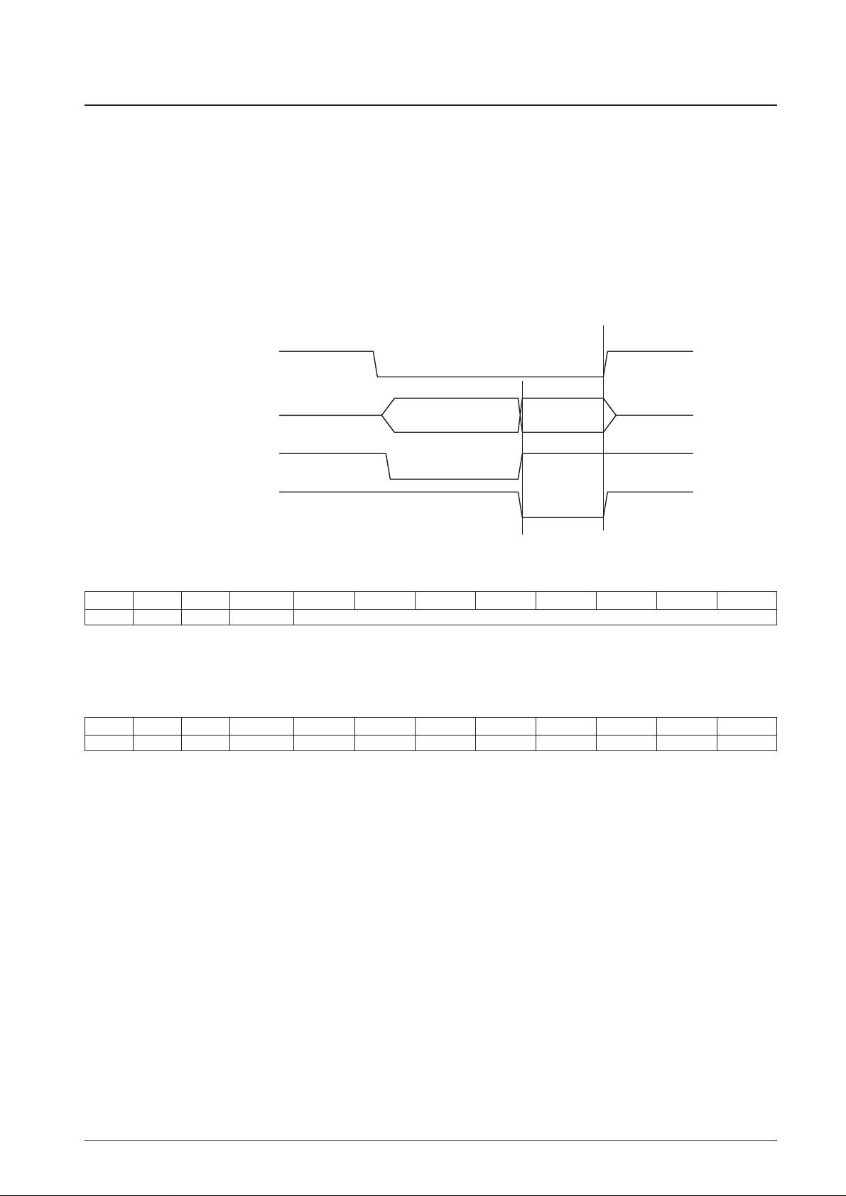
• SUBBLK
0: Normal status. (default)
1: Set to 1 when a substation (for example a dGPS station during VICS reception) is temporarily received.
Valid
output
RD
RDY
timing 1
timing 2
RDY
DATn
RDY Signal Output Timing
This is the data group write register used for the layer 4 CRC check. It is used only when the parallel interface is used.
Applications should specify the dedicated CCB address when using the serial interface.
Layer 4 CRC Register
Address Register R/W Initial value BIT7 BIT6 BIT5 BIT4 BIT3 BIT2 BIT1 BIT0
06H CRC4 W 00H (LSB)
Status Register
Address Register R/W Initial value BIT7 BIT6 BIT5 BIT4 BIT3 BIT2 BIT1 BIT0
01H STAT R — VH BLK FRM ERR PRI HEAD CRC4 RTIB
•VH
0: Indicates data for which only horizontal correction was performed.
1: Indicates data for which after horizontal correction, vertical and then second horizontal correction were performed as
well.
Packet data with an RTIB flag is output with VH set to 0.
• BLK
0: Indicates data that was received with block synchronization unsynchronized.
1: Indicates data that was received with block synchronization synchronized.
• FRM
0: Indicates data that was received with frame synchronization unsynchronized.
1: Indicates data that was received with frame synchronization synchronized.
• ERR
0: Indicates data for which error correction completed and no errors were detected in the level 2 CRC check.
1: Indicates data for which error correction was not possible or for which errors were detected in the level 2 CRC
check.
• PRI
0: Indicates data that was inferred to be data block data by the frame synchronization circuit.
1: Indicates data that was inferred to be parity block data by the frame synchronization circuit.
Packet data with an RTIB flag is output with PRI set to 0.
Page 15

No. 6167-15/29
LC72711W, 72711LW
• HEAD
0:
1: Indicates data that was inferred to be in the frame head block by the frame synchronization circuit.
This flag is valid only when VH is 0.
• CRC4
0: Indicates that the layer 4 CRC detection circuit division registers were not all zeros.
1: Indicates that the layer 4 CRC detection circuit division registers were all zeros, i.e. that there were no errors.
The result at the point immediately prior to register readout is loaded into this flag.
• RTIB
0:
1: Indicates the data is a real-time information block. (This bit is valid only in method A'.)
This bit is fixed at 0 during method A and method B reception.
Indicates the block number or the parity block number of the output data.
A single frame consists of data blocks numbered 0 to 189 and parity blocks numbered 0 to 81. Output following vertical
correction does not include parity block data.
The value of the block number register is undefined if VEC_HALT (bit 2 in control register 1) is set to 1.
Data Update Timing for Read Registers
The data in the two read registers (the status register at address 01H and the block number register at address 02H) is
updated in the 1 ms interval between 1 ms prior to the output of the interrupt control signal (INT) and a point
immediately before the INT output.
In normal processing, when an interrupt occurs, the application will first determine the nature of the data packet that will
be output by the current interrupt signal by reading out the status register, and determine if it is necessary to read out that
data. For example, if error correction failed and the erroneous data is not required, the application should simply wait for
the next interrupt.
If the CCB interface is used, the application reads out the data from CCB address #FB, and determines the status from the
additional 16 bits of data. It then either reads out the following data or sets the CE signal low to cancel the readout.
Applications can also read out data asynchronously with respect to the interrupt signal. In this case, the application
checks the current reception status by reading out the status register and checking bit 6 (data received in the block
synchronized state) and bit 5 (data received in the frame synchronized state). In this case, using data for which bit 7 (VH)
is 0 provides superior real time characteristics.
Block Number Register
Address Register R/W Initial value BIT7 BIT6 BIT5 BIT4 BIT3 BIT2 BIT1 BIT0
02H BLNO R — BLN7 BLN6 BLN5 BLN4 BLN3 BLN2 BLN1 BLN0
Page 16

No. 6167-16/29
LC72711W, 72711LW
CPU Interface Timing <Parallel Mode>
• Register Read Timing
t
CYRD
t
WRDL1
, t
WRDL2
A0 to A3
CS
t
HARD
t
SARD
t
DRDY
t
RDH
t
WRDY
Valid
output
RD
RDY
DATn
* t
HARD
stipulates the earliest timing for A0 to A3 and CS.
• Register Write Timing
t
CYWR
t
WWRL
A0 to A3
CS
t
HAWR
t
WDH
t
SAWR
WR
DATn
Page 17

No. 6167-17/29
LC72711W, 72711LW
• Post-Correction Data Read Timing
t
CYRD
t
WDRD1
, t
WDRD2
A0 to A3
CS
t
SARD
t
DRDY
t
RDH
t
WDRDY
Valid
output
Valid
output
RD
RDY
DATn
*: A0 to A3: When post-correction data is read,
A0 to A3 will be held fixed at 0.
• Post-Correction Data Read Timing (DMA)
t
WRDM
t
DREQ
*:
*:
*:
A0 to A3: When post-correction data is read, A0 to A3 will be held fixed at 0.
DREQ and DACK: The polarity of these signals can be set.
Applications can select whether the DR or DACK signal is used for readout.
A0 to A3
DACK
DREQ
CS
t
CYDM
t
RDH
RD
DATn
Page 18

No. 6167-18/29
LC72711W, 72711LW
Layer 4 CRC Detection Circuit <Parallel Interface>
This function provides data group error detection, i.e. layer 4 CRC. When the stipulated number of bytes of data group
data and the CRC detection word (16 bits) are written to the layer 4 CRC register (address 6), if either the CRC4 pin
outputs a high level or the CRC4 flag (bit 1 in the status register at address 1) is set to 1 then there were no errors in the
data. The CRC4 pin or CRC4 flag in the status register outputs a high level, if the IC internal CRC detection register bits
are all in the logic 0 state.
When this function is used to perform a layer 4 CRC check, applications must initialize the IC internal CRC detection
register before transferring the data for a single data group. This initialization is performed by sending data for bit 7
(CRC4_RST) in control register 1. Note that since this initialization flag is not automatically reset to 0, after the
application sets this flag it must then send another data item that resets it to 0 before sending the layer 4 CRC check data.
If there were no errors in all the received data groups, the CRC register will, necessarily, be all zeros after the CRC check
for a given data group. Therefore, as long as there are no errors detected in the layer 4 CRC check, the application does
not need to initialize the CRC detection register again using the control register as described above. There is no upper
limit on the total data length of data groups that can be transferred. Also, when the serial interface issued, the CCB
transfers can be divided into multiple transfer operations. The generating polynomial G(x) for the CRC code is as
follows. G(x) = X16+ X12+ X5+ 1
Structure of the Post-Correction Output Data <Parallel Interface>
The total length of the prepared output data is always 176 bits, i.e. 22 bytes. The layer 2 CRC data (14 bits) and the parity
data (82 bits) are not output. The data in each packet in the post-correction data is output in order starting at the
beginning in 8- or 16-bit units. BIC codes are not output.
When the CPU reads out the data, it can easily select the data by checking the status register first. The CPU can then
simply ignore data determined to be unnecessary without having to read it out by simply waiting until the next interrupt
arrives.
Structure of a Single Data Packet (Total length: 272 bits. BIC is not included.)
Data block (176 bits) Post-error correction data
*: This data is not output.
CPU Interface <CCB Mode>
CCB Format
Data is input and output using the CCB (Computer Control Bus) format, which is Sanyo’s audio IC serial bus format.
This IC uses an 8-bit address CCB with the address shown below. The CCB address is sent while CE is low, and the
CCB I/O mode is determined when CE is set high.
Data Input (Register Write)
Data is stored in an IC internal register. The CCB address #FA and 16 bits of data (DI0 to DI15) are input to the DI pin.
The bits are assigned as follows. Although DI12 to DI15 are unused data, arbitrary values must be provided to complete a
full 16 bits of data.
See the “Control Register” section earlier in this document for details on the register contents and addresses.
Details on writing to the layer 4 CRC check register are described later in this document. (The CCB address #FC is used
for this function.)
I/O mode
CCB address
Item
B0 B1 B2 B3 A0 A1 A2 A3
Input 0 1 0 1 1 1 1 1 16-bit control data input
Output 1 1 0 1 1 1 1 1 Data corresponding to the number of clock (CL) cycles is output
Input 0 0 1 1 1 1 1 1 Data input mode for the layer 4 CRC detection circuit (8-bit units)
Output 1 0 1 1 1 1 1 1 Register output only
DI0 DI1 DI2 DI3 DI4 DI5 DI6 DI7 DI8 DI9 DI10 DI11 DI12 to DI15
BIT0 BIT1 BIT2 BIT3 BIT4 BIT5 BIT6 BIT7 BIT0 BIT1 BIT2 BIT3
Unused data
(LSB) Input data (8 bits) (MSB) Register address
Layer 2 CRC (14 bits)
Parity (82 bits)
Page 19

No. 6167-19/29
LC72711W, 72711LW
Internal data latch operation
t
EL
t
EH
t
ES
t
CL
t
LC
t
CH
t
HD
t
SU
A3 DI15DI14DI13DI2DI1DI0A2A1A0B3B2B1B0
DI
CL
CE
Data Output (Post-Correction Data Output)
The IC outputs packet data to which error correction processing has bee applied. The application inputs the CCB address
#FB to DI.
*: The DO pin is normally left open.
Since the DO pin is an n-channel open-drain output, the data change time from a low-level
output to a high-level output differs due to the pull-up resistor.
t
EL
t
DDO
t
ES
t
CL
t
CH
t
HD
t
SU
A3
DO287DO286DO285
DO2DO1DO0
A2A1A0B3B2B1B0
DI
DO
CL
CE
Structure of the Post-Correction Output Data <CCB Interface>
Post-error correction data can be output by using CCB address #FB. Although there are up to 288 bits of valid data that
can be output, it is possible to stop clock input (CL input) and set CE to the low level, and output the remaining data on
the next interrupt with no harmful effects whatsoever.
• The maximum amount of data that can be output is 288 bits (36 bytes), and the contents of the status register (STAT)
and the block number register (BLNO) are added as the first two bytes.
• The contents of the STAT and BLNO registers are output LSB first.
• The post-correction data is output in order starting with the first bit in each single block of data.
• The BIC code is not output.
• The values of the output data are not guaranteed if multiple data read operations are performed for a single interrupt
signal (INT).
STAT (8 bits) BLNO (8 bits) Data section (176 bits) Post-error correction data
Layer 2 CRC (14 bits)
Parity (82 bits)
DO0 to DO7 DO8 to DO15 DO16 to DO191 DO192 to DO205 DO206 to DO287
Page 20

No. 6167-20/29
LC72711W, 72711LW
CRC4 pin output after N items
have been transferred.
Note: The number of items, N, refers to
the number of 8-bit items.
t
EL
t
EH
t
ES
t
CL
t
CRC
t
CH
t
HD
t
SU
A3 NN-1N-2CR2CR1CR0A2A1A0B3B2B1B0
DI
CRC4 pin output
CL
CE
Layer 4 CRC Check Circuit <CCB Interface>
The basic outline of this operation is the same as that described in the Layer 4 CRC Detection Circuit <Parallel
Interface> section earlier in this document. The data group data used for this error detection operation is sent to the IC
using the CCB interface. The value #FC is used as the CCB address.
The data group data is transferred in 8-bit units. There is no upper limit on the amount of data that can be transferred (the
value N in the figure below), and the data transfer may be divided into multiple operations.
t
EL
t
DDO
t
ES
t
CL
t
CH
t
HD
t
SU
A3
BLN7BLN6BLN5ST2ST1ST0
A2A1A0B3B2B1B0
DI
DO
CL
CE
Register Output
The IC internal status and block number registers are special-purpose registers that can be read out by applications. (See
the discussion of the read register data update timing on page 15.)
The application inputs the CCB address #FD to DI. The status register data is output first followed by the block number
register data.
Page 21

No. 6167-21/29
LC72711W, 72711LW
VDD voltage
RST
3.4 V (2.5 V in the LC72711LW)
V
IL
(0.3*VDD)
V
IH
300 ns (min)
Notes on Operation during Resets and in Standby Mode
Reset Signal
The reset operation is executed when the supply voltage (VDD) rises above 3.4 V (2.5 V in the LC72711LW) and the
RST pin input level is held at or below VILfor 300 ns or longer. (See the figure below.)
When power is first applied, or when power is removed and applied again, always apply a reset before using this IC.
Pin States during Reset
Low level:CLK16 (5), DATA (6), FLOCK (7), BLOCK (8), FCK (9), BCK (10)
High level: INT (33), RDY (16), CRC4 (11), DREQ (12)
Open: D0 (17) to D15 (32), DO (36)
Reset Operating Range
The states of the output pins as the result of a reset signal are stipulated in the "Pin States during Reset" item above. The
IC internal flip-flops are all reset. While the shift registers used for delay are also reset, the memory array is not
influenced by this operation. However, since memory is not refreshed, data cannot be retained. The crystal oscillator
circuit is not stopped.
Post-Reset Data Input
After a reset operation has completed, if at least one clock cycle (about 278 ns when the IC's main clock is 3.6 MHz)
elapses, the register write circuit will be functional. (That is, the IC can accept data.)
Notes on Standby Mode
The IC is set to standby mode by applying a high level to the STNBY pin. Since all IC operations are stopped in this
mode, the state is essentially equivalent to removing power from the IC. (Note that after clearing standby mode,
applications must wait the oscillator stabilization time before using the IC.)
The pin output states during standby mode are the same as those states during a reset as described above.
Output Conditions for Post-Error Correction Output (Default Mode)
(1) For each block (272 bits) of received data, the IC applies (272, 190) code error correction and a layer 2 CRC error
check. After the error correction has completed, the IC prepares to transfer the data to the CPU and outputs an
interrupt signal from the INT pin. This is referred to as horizontal correction output.
(2) Note that under the default operating conditions, this interrupt signal is not output unless the corresponding output
data meets the following three conditions.
• Error correction completed correctly and no errors were discovered in the layer 2 CRC check.
• The data was received in both block and frame synchronization.
• The data is packet data.
(3) If the data could not be corrected in horizontal correction, product code correction is performed in frame units and
a second horizontal correction operation is performed for this data that could not be corrected by the first
horizontal correction. This sequence of operations is called vertical correction.
The output conditions for data that can be acquired after vertical correction are as follows.
• The data that could not be corrected by horizontal correction only, but that was corrected by vertical correction.
• The data is packet data.
Page 22

This means that data that was fully corrected by horizontal correction is not output. Also, packet data that could
not be corrected by either horizontal correction or vertical correction is not output. Furthermore, post-vertical
correction parity packet data is also not output.
(4) Applications can clear the INT signal selection conditions described in (2) and (3) above by setting bit 5
(INT_MOVE) in the control register.
(5) Vertical correction is performed when all of the packet data in a frame is received in frame synchronization and
furthermore when it was not possible to correct all of the packet (block) data with horizontal correction.
Vertical correction is not performed if one frame of data with no errors was received or the receiver was not in
frame synchronization during reception.
To prevent incorrect correction, error correction using vertical correction is not performed for packets error
correction using horizontal correction fully completed and for packets that had no errors.
(6) Under the default settings, if vertical correction is not performed, the corresponding post-vertical correction output
is not output.
Applications can specify the post-vertical correction data to be output regardless of whether or not vertical
correction is performed by setting bit 2 (VEC_OUT) in control register 2.
Note 1. In this case, if data with absolutely no errors is received, completely identical data will be output twice,
once as horizontal correction output, and once as vertical correction output. This status is identical to the
output status of the LC72700E.
Note 2. Immediately after power is applied, undefined data that is, in principle, not required by applications, will
be output as post-vertical correction data.
CPU Interface Basic Limitations
To save internal memory, this IC limits its output data buffer to the smallest size possible. Since the data received by the
IC is written to memory continuously without interruption, the post-correction data in the output data buffer that should
be read out may be overwritten by the following data if readout of the data is delayed.
The output timing for post-correction data, both horizontal and vertical, is stipulated as follows for this IC.
(1) When the IC completes preparation of the output data, it drops the INT pin to the low level as a transfer request.
(2) During data output, there are periods when only horizontal data can be read out, and there are other periods when
both horizontal data and vertical data can be read out in a time-division multiplexed manner.
(3) Applications must complete the data transfer operation within 9 ms after the INT pin goes low. If only post-
horizontal correction data is output, the data transfer may be performed within an 18 ms period.
After the stipulated period, the next data will be written to the output buffer replacing the previous data, even if
the CPU is reading out the data.
(4) The amount of data that can be read for a single transfer request (INT) for each of the horizontal and vertical data
is one block only. The post-vertical correction data is output in order starting with block number 1 after vertical
correction processing completes. The parity block data is not output.
No. 6167-22/29
LC72711W, 72711LW
18 ms
1 ms
INT
Horizontal data only
output
Horizontal and vertical
data output
Horizontal data
output period
Vertical data
output period
Horizontal data
output period
Period during which data
retention is not guaranteed
68 µs
68 µs
Figure 2 External Interface - Basic Timing
Page 23

Notes on Data Output Timing (Relationship with the received data)
Figure 3 shows the timing relationship between the received data and the interrupt control signal (INT). However, the
delay from the actual received signal due to demodulation operations in MSK demodulation blocks is ignored.
Block synchronization is established by discriminating the BIC code. As shown in figure 3, the data for the nth packet
can be output during reception of the following packet (number n+1).
Figure 4 shows the output timing for post-vertical correction data. In vertical correction, the data for a single frame is
stored in memory and the correction operation is performed if frame synchronization was established and it was not
possible to correct all the packet data in horizontal correction. The timing with which vertical correction is started is the
start of the frame. Horizontal correction is performed for each packet while packets 1 through 28 in the nth frame are
being received, and this data is passed to the CPU interface. Vertical correction is performed for the data from the
previous frame (frame n-1) in the unused time periods during that processing.
The vertical correction data consists of 190 blocks that are output, and this data is output at the rate of one block for
every block received, in order starting at the time the 29th packet (block) is received. Only data from the data blocks in
the FM multiplex broadcast frame structure is output, and the last block (block 190) is output during reception of the
218th block.
As indicated previously (page 21) packet data that was, for example, corrected completely by horizontal correction, is not
output in the vertical correction output data. (The INT signal is not issued.) However, the order in which the horizontal
output is produced is not speeded up by the amount of the packet data that is not output. For example, if data packets 1 to
100 were corrected by horizontal correction, output of the post-vertical correction packet data for packet 101 will not
occur at the reception position of block number 29 in figure 4, but at the reception position for packet data number 129.
No. 6167-23/29
LC72711W, 72711LW
BICBIC
18 ms
300 ns max
300 ns max
Packet n-1 Packet n+1
Packet n data
1 ms
Received
data
BCK
INT
Data cannot
be guaranteed
Packet n data output
Output period for
packet n+1 data
62.5 µs
68 µs
Figure 3 Received Data, Block Synchronization, and Data Output Timing
First
frame
BCK
FCK
INT
Output periods for
post-vertical correction
data from the previous
frame.
62.5 µs
Received block
signal
nth frame
18 ms × 28 = 504 ms
189 19021
271 272 1 2 3 28 29 30 31 220219218
18 ms
1 ms
18 ms
9 ms
9 ms
Figure 4 Post-Vertical Correction Data Output Timing
Page 24

CPU Connection Example <Parallel Interface>
This section presents examples of the connection of this IC to a CPU.
Note that care is required with respect to read timing, since the time required to read a register, and the time required to
read a post-correction data packet (22 bytes) are different.
• Normal connection
When hardware waits are applied to the
CPU, the wait time (RDY width)
requires care.
BUSWD = low: 8 bits
BUSWD = high: 16 bits
No. 6167-24/29
LC72711W, 72711LW
LC72711W (LW) CPU
D0 to D7
(D0 to D15)
PORT1
RST
IOCNT2
IOCNT1
WAIT
INT
CS
RD
WR
A0 to A3
WR
RD
CS
INT
RDY
DACK
DREQ
SP
BUSWD
Bus-width
8 bits
• DMA transfer mode
I/O read/write operations are used for
the normal register read and write
operations. However, programmable
wait states may need to be inserted,
depending on the execution speeds.
DMA processing is only used for
readout of post-correction data.
Applications can select whether RD or
DACK is used as the DMA read control
signal by setting a register.
The default is to use the RD signal.
The data bus width in DMA mode is
always 8 bits.
CPU DMA mode setting example (For
reference only)
SH Series: Transfer type: 2-cycle
transfer
Transfer mode: Single
transfer mode
V Series: Address mode: Dual
address mode
Bus mode: Cycle
stealing mode
The source side (the FM multiplex IC)
address is fixed at 0.
LC72711W (LW) CPU
D0 to D7
PORT1RST
IOCN
T2
IOCNT1
DACK
DREQ
INT
CS
RD
WR
A0 to A3
WR
RD
CS
INT
RDY
DACK
DREQ
SP
BUSWD
Bus-width
8 bits
Page 25

• Data bus I/O control block
The data bus (D0 to D15) can be controlled with two control signals: IOCNT1 and IOCNT2.
These pins must be held low if unused.
CPU Connection Example <CCB Interface>
*: SCK, TX, and RX are the CPU serial interface channel. Normally, I/O port pins may be used for these lines.
* The resistance of the DO pin pull-up resistor must be selected according to the transfer clock speed.
No. 6167-25/29
LC72711W, 72711LW
CS
IOCNT1
IOCNT2
RD
DACK
D0 to D15
Control register 2, bits 1 and 2
LC72711W (LW)
CPU
PORT3
(INT)
PORT2
SCK *
TX *
RX *
PORT1
RST
A2/DI
A0/CL
A1/CE
INT
DO
SP
Page 26

Control Program Compatibility
This IC allows the majority of the control software used to be compatible with Sanyo's other FM multiplex ICs, in
particular, the LC72700E, LC72705E, LC72706E, LC72708E, and LC72709E(W). However, the following aspects of
the control software require modification.
• Values of the register addresses
The addresses of the allowable BIC error count, synchronization error protection count, control registers, the layer 4
CRC register, and other registers have been modified.
The CCB address for serial I/O over a CCB bus has not been changed.
• INT signal output timing
The INT signal output timing for data output is as follows. A circle ("O") indicates that INT is output, and a cross ("X")
indicates that the signal is not output.
Notes on Output Data Selection after Tuning (Reference)
When building an FM multiplex reception system, a tuning system is an absolute necessity. However, if it is
unacceptable for the IC to output data from the old station after tuning to a new station, the application must perform the
following processing.
(1) At the same time as tuning a new station, the application must set bit 4 (SYNC_RST) in control register 1 to set the
synchronization circuit to the unsynchronized state.
(2) Under the default settings, after the synchronization reset applications must acquire data according to the issued INT
signal.
The post-vertical correction output is not provided by the IC until frame synchronization has been established for the
new station after tuning and the first vertical correction operation has been performed.
(3) If bit 2 (VEC_OUT) in control register 2 has been enabled, applications must not use the post-vertical correction
output (data for which bit 7 in the status register is high) until frame synchronization has been reestablished.
This IC performs the portion of the DARC FM multiplex processing through layer 2 error correction without requiring
any special control operations. The IC itself cannot determine if the contents of the received data have changed or if a
new station has been tuned. This means that applications must use the procedure described above for this IC not to output
old data and only output the new data. Another point is that in IC synchronization, although it is rare for the old station
and the new station to be frame synchronized, applications need to perform the processing in item 1 above to cancel
frame synchronization forward protection period.
Notes:1. Data for which horizontal correction failed, but for which vertical correction succeeded is output.
2. All data is output.
3. If there is data for which horizontal correction failed, the post-vertical correction data for that data is output, regardless of whether or not vertical
correction succeeded.
(If the IC performs vertical correction, post-vertical correction data will be output.)
No. 6167-26/29
LC72711W, 72711LW
Control Control Horizontal correction output
Vertical correction output
Item
register 1 register 2
Operational overview
Correct Incorrect Parity Correct
NG
bit 5, bit 2,
data data data
INT_MOVE VEC_OUT
Default value L L
Operation identical to that of the LC72705/06/07E
●● ××●● *
1
×
and LC72708/09E(W)
Combination 1 H H
Operation identical to that of the LC72700E
●● ●● ●● ●● *
2
●●
All data is output
The output data selection conditions are cleared,
Combination 2 H L but there is no vertical correction output when ●● ●● ●● ●● *
3
●●
vertical correction is not performed
Combination 3 L H
The output data selection conditions are retained,
●● ××●● ●●
but all of the vertical correction output is output
Page 27

Sample Data Acquisition Flowchart
Note: The figure below is for allocation of received data at the layer 3 level.
This documentation is present as an example for reference purposes only of FM multiplex data acquisition
processing by the system CPU. Its operation is not guaranteed.
No. 6167-27/29
LC72711W, 72711LW
INT
End
Status acquisition
Correction
complete?
Synchronized?
Read in the postcorrection data (22 bytes)
Was this
post-horizontal
correction data?
Prefix discrimination
Prefix discrimination
Is the data
group complete?
Is the data
group complete?
Is the decoding
identifier 1?
Start decoding and
presentation processing
Layer 4 CRC check
Start decoding and
presentation processing
Layer 4 CRC check
Yes
Yes
Yes
Yes
** This discrimination is not required with the
default settings. (No INT signal is issued.)
Page 28

Additional Notes
In addition to the above processing, processing required for layer 3 (data group) level processing includes “deletion of
inappropriate data.” Although rare, in certain cases the IC will send inappropriate packet data that does not belong to any
data group currently being broadcast. The following three points are possible reasons for this occurring.
(1) The IC frame synchronization circuit generates an incorrect synchronization state, and the IC incorrectly outputs
parity packet data as normal packet data. This can occur when the back protection count is less rigorous (2 or lower),
or during weak field reception.
(2) While extremely rare, incorrect correction can occur. (This almost never happens.)
(3) Noise entering the data transfer lines between the FMD IC and the CPU within the end product set.
Inappropriate packet data that occurs for these reasons and does not belong to any data group, will not be updated, and
will remain in the program storage memory indefinitely. If the application does not include a routine that searches for and
deletes inappropriate data, program storage memory will overflow at some point.
Also, applications should perform a layer 4 CRC check after data group completion and before program display.
No. 6167-28/29
LC72711W, 72711LW
Prefix discrimination
Is the data
group complete?
Is this the
data group for the
first reception?
Resend?
Update?
End
Store in the corresponding
data group storage area.
Check the correctness of
the received data packet.
Update the data in the
existing data storage area.
Allocate a storage area
the size of the data group.
Yes
Yes
No
No
Yes
Yes
Page 29

PS No. 6167-29/29
LC72711W, 72711LW
This catalog provides information as of January, 2000. Specifications and information herein are subject
to change without notice.
Specifications of any and all SANYO products described or contained herein stipulate the performance,
characteristics, and functions of the described products in the independent state, and are not guarantees
of the performance, characteristics, and functions of the described products as mounted in the customer’s
products or equipment. To verify symptoms and states that cannot be evaluated in an independent device,
the customer should always evaluate and test devices mounted in the customer’s products or equipment.
SANYO Electric Co., Ltd. strives to supply high-quality high-reliability products. However, any and all
semiconductor products fail with some probability. It is possible that these probabilistic failures could
give rise to accidents or events that could endanger human lives, that could give rise to smoke or fire,
or that could cause damage to other property. When designing equipment, adopt safety measures so
that these kinds of accidents or events cannot occur. Such measures include but are not limited to protective
circuits and error prevention circuits for safe design, redundant design, and structural design.
In the event that any or all SANYO products (including technical data, services) described or contained
herein are controlled under any of applicable local export control laws and regulations, such products must
not be exported without obtaining the export license from the authorities concerned in accordance with the
above law.
No part of this publication may be reproduced or transmitted in any form or by any means, electronic or
mechanical, including photocopying and recording, or any information storage or retrieval system,
or otherwise, without the prior written permission of SANYO Electric Co., Ltd.
Any and all information described or contained herein are subject to change without notice due to
product/technology improvement, etc. When designing equipment, refer to the “Delivery Specification”
for the SANYO product that you intend to use.
Information (including circuit diagrams and circuit parameters) herein is for example only; it is not
guaranteed for volume production. SANYO believes information herein is accurate and reliable, but
no guarantees are made or implied regarding its use or any infringements of intellectual property rights
or other rights of third parties.
• The DARC (Data Radio Channel) FM multiplex broadcast technology was
developed by NHK (Japan Broadcasting Corporation).
• DARC is a registered trademark of NHK Engineering Service (NHK-ES).
• A separate contract with NHK-ES is required in advance for the manufacture
and/or sale of electronic equipment that uses DARC technology.
• The logo shown here can be displayed on electronic equipment that uses DARC
technology.
• Sanyo Electric Co., Ltd. has reported to NHK-ES the number of units and purchasers of ICs that use DARC technology shipped
since October 1997.
 Loading...