

Page 1
SANYO Electric Co.,Ltd. Semiconductor Bussiness Headquarters
TOKYO OFFICE Tokyo Bldg., 1-10, 1 Chome, Ueno, Taito-ku, TOKYO, 110 JAPAN
Overview
The LC72700E and LC72700G are data decoder LSIs for
receiving DARCTMmobile FM multiplex broadcasts. A
multi-function, compact, adjustment-free system can be
implemented in two chips by combining this LSI with the
LV3400M band-pass filter IC, which extracts the
multiplex components from a composite FM signal.
Functions and Features
• Delay detection scheme using a 1T delay
• Built-in error correction function using a 2T delay
• Digital PLL clock regeneration
• Block and frame synchronization detection with a
settable synchronization protection count
• Settable block identifier code (BIC) detection precision
• Error correction using (272,190) codes
• Built-in frame memory for product codes
• Support for both serial and parallel data I/O
• Package
LC72700E: QFP48E
LC72700G: QFP48G
CMOS LSI
Ordering number : EN4870E
63097HA (OT)/D3095HA (OT)/D1594TH (OT) No.4870-1/14
SANYO: QFP48E
[LC72700E]
SANYO: QFP48G
[LC72700G]
SANYO Electric Co.,Ltd. Semiconductor Bussiness Headquarters
TOKYO OFFICE Tokyo Bldg., 1-10, 1 Chome, Ueno, Taito-ku, TOKYO, 110 JAPAN
Mobile FM Multiplex Broadcast Receiver LSI
LC72700E, LC72700G
Specifications
Absolute Maximum Ratings at Ta = 25°C
Parameter Symbol Conditions Ratings Unit
Maximum supply voltage V
DD
max V
DD
–0.3 to +7.0 V
Input voltage
V
IN
1 CL, CE, and DI pins –0.3 to +7.0 V
V
IN
2 Input pins other than VIN1 –0.3 to VDD+ 0.3 V
Output voltage
V
OUT
1 DO pin –0.3 to +7.0 V
V
OUT
2 Output pins other than V
OUT
1 –0.3 to VDD+ 0.3 V
Output current I
OUT
BCLOCK, FCLOCK, and DO pins 0 to 4.0 mA
Allowable power dissipation Pd max Ta ≤ 85°C 400 mW
Operating temperature Topr –40 to +85 °C
Storage temperature Tstg –55 to +125 °C
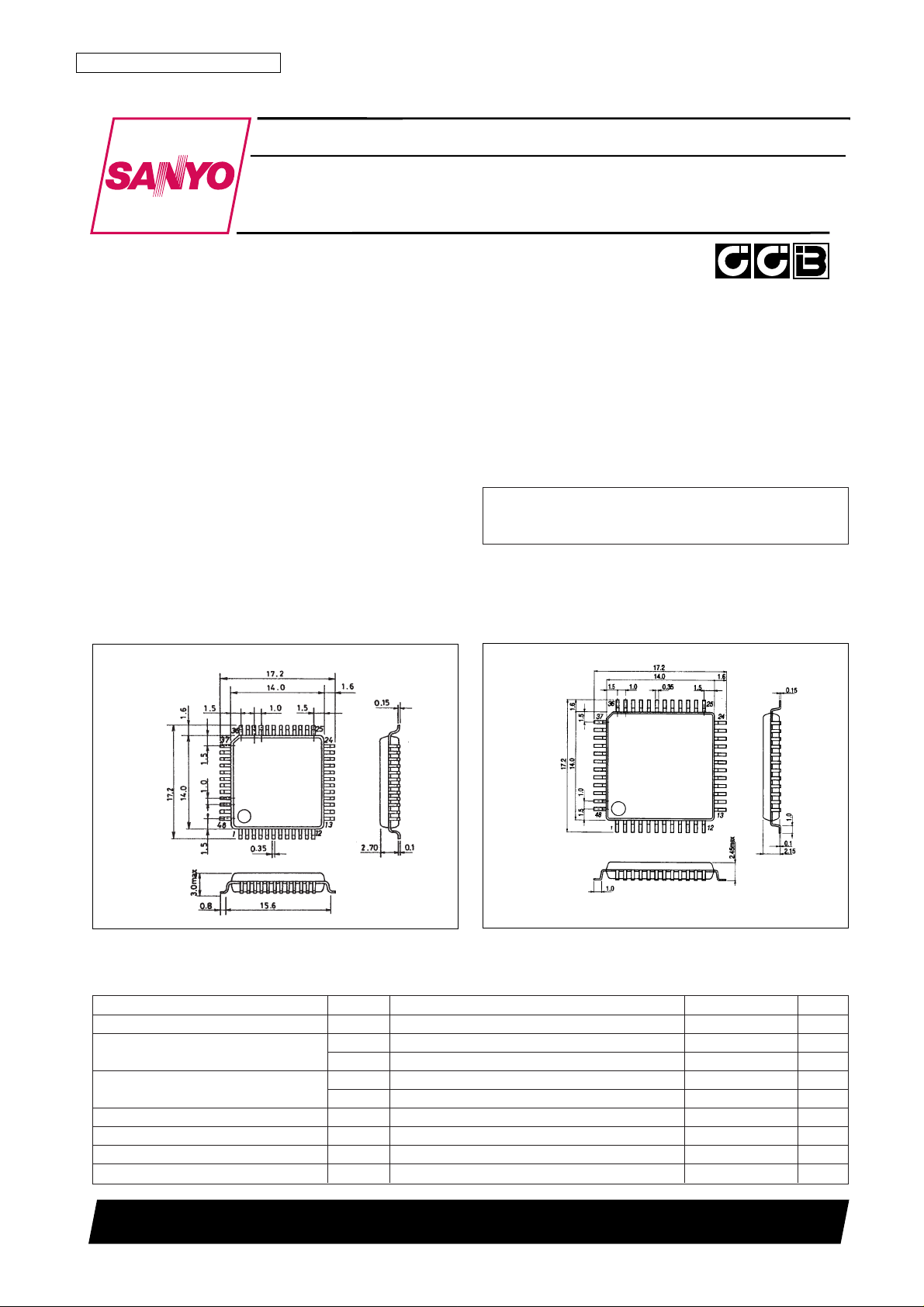
Package Dimensions
unit: mm
3156-QFP48E
unit: mm
3229-QFP48G
• CCB is a trademark of SANYO ELECTRIC CO., LTD.
• CCB is SANYO’s original bus format and all the bus
addresses are controlled by SANYO.
Page 2
Allowable Operating Ranges at Ta = –40 to +85°C, VSS= 0 V
Note: 1. This LSI operates at a frequency of 7.2 MHz ±250 ppm.
2. See the parallel data timing.
3. See the parallel data timing.
Electrical Characteristics in the Allowable Operating Ranges
No. 4870-2/14
LC72700E, LC72700G
Parameter Symbol Conditions min typ max Unit
Supply voltage V
DD
V
DD
4.5 5.0 5.5 V
V
IH
1
MSK, DAT0 to 7, RE, PST, S/P, PORT0 to 2, RST,
0.7 V
DD
V
DD
V
Input high level voltage
TEST1, TEST2
V
IH
2 CL, CE, DI 0.7 V
DD
5.5 V
V
IL
1
MSK, DAT0 to 7, RE, PST, S/P, PORT0 to 2, RST,
V
SS
0.3 V
DD
V
Input low level voltage
TEST1, TEST2
V
IL
2 CL, CE, DI V
SS
0.3 V
DD
V
Oscillator frequency F
OSC
*
1
7.2 MHz
Input sensitivity V
XI
XIN, sine wave, capacitive coupling 400 1500 mVrms
Serial I/O
*2
Clock low level time t
CL
CL 0.7 µs
Clock high level time t
CH
CL 0.7 µs
Data setup time t
SU
CL, DI 0.7 µs
Data hold time t
HD
CL, DI 0.7 µs
CE wait time t
EL
CL, CE 0.7 µs
CE setup time t
ES
CL, CE 0.7 µs
CE hold time t
EH
CL, CE 0.7 µs
Data latch switching time t
LC
0.7 µs
Data output time t
DDO
DO, CE 277 555 ns
Parallel I/O
*3
RE wait time t
RE
RE 1 µs
RDY wait time t
DRD
RE, RDY 0.5 0.8 µs
RDY output time t
RDY
RDY 2.2 µs
PST input time t
PS
PST 0.3 µs
PST hold time t
PH
PST, DAT0 to 7, PORT0 to 2 10 ns
I/O direction switching time
t
DIR
PST, DAT0 to 7 0.5 0.8 µs
Parameter Symbol Conditions min typ max Unit
V
OH
1 IO= 1 mA, FILCK, CLK, DATA VDD– 1.0 V
High level output voltage
V
OH
2
I
O
= 2 mA, DAT0 to 7, BCLOCK, FCLOCK, BL-CK,
V
DD
– 0.4 V
FC-CK, INT-R, RDY, RDY0
Low level output voltage
V
OL
1 IO= 1 mA, for the VOH1 applicable pins 1.0 V
V
OL
2 IO= 2 mA, for the VOH2 applicable pins 0.4 V
V
OL
3 IO= 2 mA, DO 0.4 V
I
IH
1 VIN= 5.5 V, CE, CL, DI 1 µA
High level input current
I
IH
2 VIN= VDD, input pins except IIH1 1 µA
I
IL
1 VIN= VSS, CE, CL, DI –1 µA
Low level input current
I
IL
2
V
IN
= VSS, inputs with pull-up resistors, RE, PST,
–100 µA
PORT0 to 2, S/P
I
IL
3 V
IN
= V
SS,
MSK, RST –1 µA
Output off leakage current I
OFF
VO= V
DD,
DO 5 µA
Hysteresis voltage V
HIS
MSK, CL, CE, DI, RST 0.1 V
DD
V
Built-in feedback resistance Rf XIN, XOUT 1.0 MΩ
Pull-up resistance Rpu RE, PST, PORT0 to 2, S/P 50 kΩ
Current drain I
DD
16 25 mA
Page 3
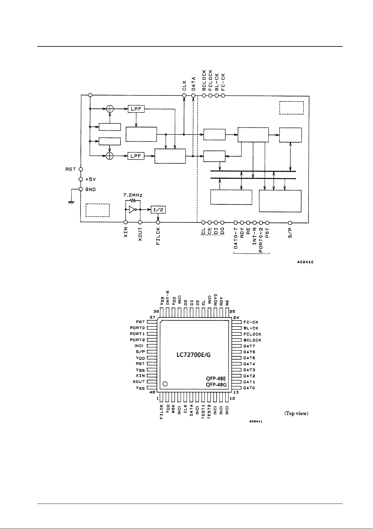
Block Diagram
Pin Assignment
No. 4870-3/14
LC72700E, LC72700G
MSK signal
input
1T delay
2T delay
Clock
regeneration
Demodulation
block
Synchronization
regeneration
PN
decoding
Timing
control
Output control
(CPU interface)
Memory cell
Error
correction
block
Error
correction
MSK error
correction
Data
Address
(Parallel I/O)
(Serial I/O)
Page 4
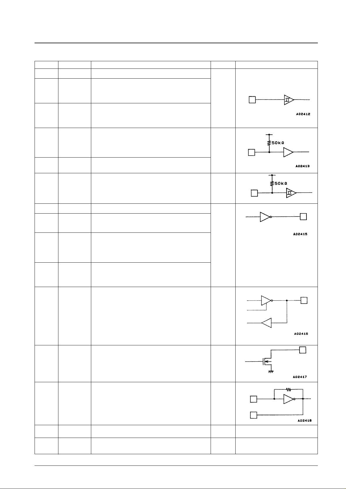
Pin Descriptions
No. 4870-4/14
LC72700E, LC72700G
Pin No. Symbol Function I/O I/O Circuit
3
29
30
31
1
5
6
21
22
23
24
26
27
35
13
14
15
16
17
18
19
20
32
46
47
2, 34, 43
36, 45, 48
4, 7, 10
11, 12, 28
33, 41
MSK
CL
CE
DI
FILCK
CLK
DATA
BCLOCK
FCLOCK
BL-CK
FC-CK
RDY
RDY0
INT-R
DAT0
DAT1
DAT2
DAT3
DAT4
DAT5
DAT6
DAT7
DO
XIN
XOUT
V
DD
V
SS
NC
76 kHz MSK signal input
CCB serial interface Clock input
Data control input
Data input
Reference clock output for the LV3400M
Clock regeneration monitor output
Demodulated data monitor output
Outputs a high level during block synchronization
Outputs a high level during frame synchronization
Block start signal output
Frame start signal output
Parallel IF data output enable signal
Parallel IF data output enable signal
Output data external CPU interrupt signal
Parallel IF data output pin 0
Parallel IF data output pin 1
Parallel IF data output pin 2
Parallel IF data output pin 3
Parallel IF data output pin 4
Parallel IF data output pin 5
Parallel IF data output pin 6
Parallel IF data output pin 7
CCB serial interface data output
System clock oscillator crystal connection
Power supply (+4.5 to +5.5 V)
Ground pin
Not connected
Output
I/O
Output
Input
Output
—
—
—
Input
44
8
9
RST
TEST1
TEST2
System reset input pin (negative logic)
Test pin 1 (normally connected to ground)
Test pin 2 (normally connected to ground)
37
38
39
40
PST
PORT0
PORT1
PORT2
Parallel IF mode data settings
Port address 0
Port address 1
Port address 2
Input
42
S/P
Serial/parallel IF switch
(Serial mode when high)
25
RE Parallel IF mode data output control signal input
Input
A02414
Page 5
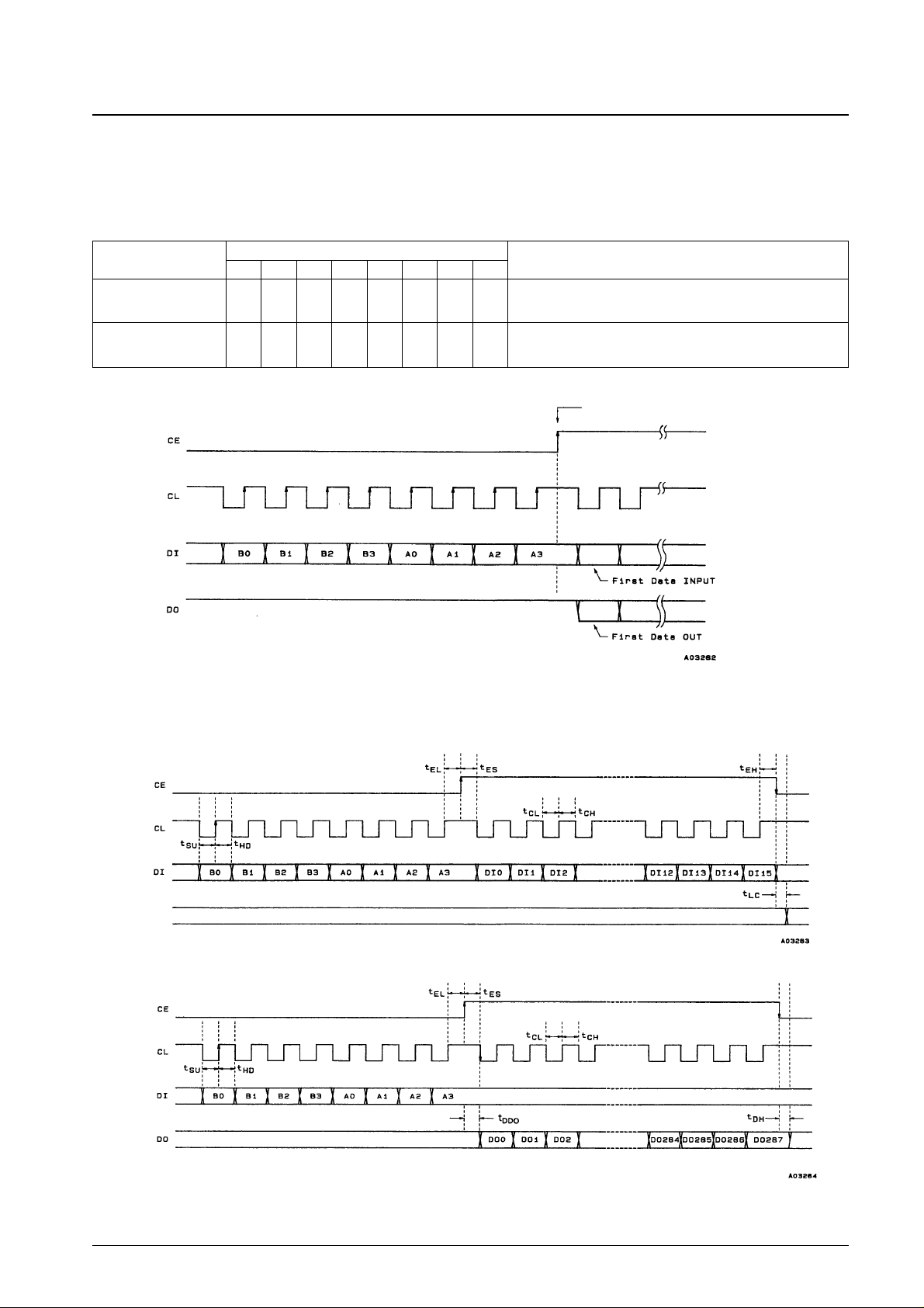
Serial Data I/O Scheme
1. CCB Format
The figure shows the Sanyo audio LSI serial bus format. Data is input and output over a CCB (computer control
bus). This LSI uses an 8-bit address CCB format.
2. Serial Data Input Timing
3. Serial Data Output Timing
Note: * The DO pin is normally open.
Since the DO pin is an n-channel open-drain output, the time for the data value to change from the low level to the high level depends on the value
of the pull-up resistor used.
No. 4870-5/14
LC72700E, LC72700G
I/O mode
Address
Function
B0 B1 B2 B3 A0 A1 A2 A3
Input
Output
0 1 0 1 1 1 1 1
1 1 0 1 1 1 1 1
16-bit control data input
Data output
Internal data
I/O mode is set.
Page 6

4. Serial Control Data Input Setting Values
The input data consists of 16 bits (DI0 to DI15) of which the upper 8 bits (DI8 to DI15) are the control address
and the lower 8 bits (DI0 to DI7) are the input data.
Note: 1. The data in address bits DI12 to DI15 is ignored.
2. The value of the data sent to set the protection count must be one less than the desired protection count. In the default example shown above, the
block forward protection count will be 8 and the frame back protection count will be 2. When the value is set to 0, the protection count will be 1.
Since a protection count of 0 is meaningless the LSI ignores this value.
3. The initial threshold value is the initial value used when executing error correction at a variable threshold. There is no need to change this value
unless some special experiment is being performed. The threshold value can be set to a value from 9 to 15 according to a three-bit field. Therefore
a data value of 7 sets the threshold value to 15 and a data value of 1 sets the threshold value to 9.
4. The readout block number is transferred when the skip function is used.
5. Addresses other than those listed above (e.g. 0101) are special addresses unique to this LSI and are for test mode and other functions. These
addresses should not be used.
6. The default values are the values loaded into internal registers when a reset signal (RST) is received. These are recommended values and do not
require modification in normal operation. If the default values are used then there will be no need to implement control microprocessor software
that inputs control data.
No. 4870-6/14
LC72700E, LC72700G
Register
Address
Data Default setting
DI11 DI10 DI9 DI8
Allowed error count 0 0 0 0
Upper 4 bits Back allowed errors 2
Lower 4 bits Forward allowed errors 2
Block error protection count 0 0 0 1
Upper 4 bits Back protection count 1
Lower 4 bits Forward protection count 7
Frame error protection count 0 0 1 0
Upper 4 bits Back protection count 1
Lower 4 bits Forward protection count 7
Error correction initial
0 0 1 1
Upper 5 bits — —
threshold value
Lower 3 bits Initial threshold value 7
Readout (output) block number 0 1 0 0 0 to 189 (8 bits) 0
Page 7

Structure of the Output Data
1. The output data consists of a total of 288 bits (36 bytes). The first two bytes are status information.
2. CNT1 and CNT2 are both output LSB first.
3. Corrected data is output in order starting with the first bit in each block.
4. The BIC code is not output.
5. These points hold for both serial and parallel mode.
*: The CPU can easily select data by first checking the content of the status information when data is read out. Data that
is not required does not have to be read; rather, the CPU can cancel the remainder of the readout operation. (The
CPU can simply ignore data until the next interrupt.)
BLN7 to BLN0: Expresses the block number or the parity block number of the output data. The block numbers within a
single frame range from 0 to 189, and the parity block numbers from 0 to 81.
Note that parity block data is not output for vertically corrected data.
No. 4870-7/14
LC72700E, LC72700G
288 bits (36 bytes)
Corrected data 272 bits (34 bytes)
*Bits 0 and 1 are unused and contain invalid data.
However, this bit is only valid when only horizontal correction is applied, i.e.
when V
H
= 0.
First block data output (Only when V
H
is low.)
Normal data
Parity data
Correction OK
Error (uncorrectable data)
Indicates data for which frame synchronization was not achieved
Indicates frame synchronized data
Indicates data for which block synchronization was not achieved
Indicates block synchronized data
Output that was only corrected horizontally (synchronized output)
Output that was vertically corrected
Page 8

Parallel Mode Data I/O Methods
Data is input and output using the parallel data interface I/O pins, INT-R (pin 35), RE (pin 25), RDY (pin 26), RDY0
(pin 27) and DATn (pins 13 to 20).
1. Basic Data Output Procedure
(1) Interrupt handling starts on the falling edge of INT-R.
(2) Set RE low.
(3) RDY goes low temporarily and then goes high on output ready.
(4) After RDY goes high, read in the data from DATn.
(5) Return RE to high.
Repeat steps (2) to (5) until 36 bytes of data have been read in.
Note: The period that RDY is low is 2.2 µs (typical). The CPU does not need to monitor RDY if it can adjust its
timing. Also, RDY0 is a signal that goes low when output is ready and goes high when RE returns to high.
The software logic for data acquisition can be simplified if the RDY (or RDY0) signal is input to the CPU
WAIT pin.
2. Parallel Data Output Timing
3. Parallel Data Output Timing Stipulations
4. Data Input in Parallel Mode
To store data in parallel mode, set the internal register address of the data to be stored in PORT0 to PORT2 (pins 38 to
40) and set the PST pin (pin 37) low. Then input the data to DATn (pins 13 to 20). The PORT0 to PORT2 inputs and the
data to be stored are acquired by the LSI on the rising edge of the PST signal. When the PST pin is low, the DAT0 to
DAT7 pins function as input pins. Note that the PST pin data store cycle must be 1 µs or longer.
See the section on page 6 serial data I/O for notes and terminology descriptions concerning the data stored.
No. 4870-8/14
LC72700E, LC72700G
INT-R
Page 9

4. Control Data Timing in Parallel Mode
Handling Pins for the Unused Mode when the CPU Interface is Specified
1. When Serial Mode is Specified
2. When Parallel Mode is Specified
Note:** 1. The data values shown above are for the state immediately following a reset operation.
2. The INT-R pin (pin 35) signal is always output regardless of the mode.
3. Since the S/P pin (pin 42) has a built-in pull-up resistor, serial mode will be selected if it is left open.
No. 4870-9/14
LC72700E, LC72700G
PORT2 PORT1 PORT0 Item Set data Default value
0 0 0 Allowed error count
Upper 4 bits Back allowed errors 2
Lower 4 bits Forward allowed errors 2
0 0 1
Block error protection
Upper 4 bits Back protection count 1
count
Lower 4 bits Forward protection count 7
0 1 0
Frame error protection
Upper 4 bits Back protection count 1
count
Lower 4 bits Forward protection count 7
0 1 1
Error correction initial
Upper 4 bits — —
threshold value
Lower 3 bits Initial threshold value 7
1 0 0 Readout block no. 0 to 189 (8 bits) 0
Pin Pin No. Pin state Handling
PST (37) Pull-up resistor input Leave open or connect to the power-supply (V
DD
)
PORT0 to 2 (38 to 40) Pull-up resistor input Leave open or connect to the power-supply (V
DD
)
DATA0 to 7 (13 to 20) Output direction (fixed at the low level) Leave open
RDY (26) Fixed at a high-level output Leave open
RDY0 (27) Fixed at a high-level output Leave open
RE (25) Pull-up resistor input Leave open or connect to the power-supply (V
DD
)
Pin Pin No. Pin state Handling
CL (29) Input pin Connect to the power supply or ground
CE (30) Input pin Connect to the power supply or ground
DI (31) Input pin Connect to the power supply or ground
DO (32) Open-drain output in the off state Connect to ground
Register set
Input data
DAT0 to 7
Output
Output
PORT0 to 2
PST
<Input direction>
tps≥ 300 ns
DAT pin I/O
direction
500 to 800 ns
Page 10

Circuit Operation at Reset
1. Reset Signal
The reset operation is executed by holding the RST pin input level under VILfor 300 ns or longer when the powersupply voltage (VDD) is over 3.4 volts. (See the figure.)
The reset operation is necessary to run this LSI.
2. Pin Outputs during a Reset
Low-level outputs: ...FILCK (1), CLK (5), DAT0 (13) to DAT7 (20), BCLOCK (21), FCLOCK (22), BL-CK (23),
FC-CK (24), D0 (32)
High-level outputs: ...RDY (26), RDYO (27), INT-R (35), XOUT (47)
Note: In serial mode, the DAT0 to DAT7 pins are held at the low level at all times. In parallel mode, these pins
output low levels during a reset.
3. Reset Operating Ranges
The output pins are stipulated to operate as described in item 2 above according to a reset signal. All the LSI internal
registers go the reset state. While the shift registers for 1T and 2T delay also go to the reset state, memory cells are
not affected. However, since the memory refresh operation is stopped, data cannot be maintained. The crystal
oscillator circuit is not stopped.
4. Data Input Following a Reset
The serial or the parallel input control circuit becomes capable of operating (accepting data) one clock cycle (about
278 ns at 3.6 MHz: i.e., the LSI's main clock) after the reset completes.
Output Data (basic operation concerning error correction)
Error correction using (272, 190) codes is performed for every block (272 bits) of received data. Data is output
immediately after error correction. This is referred to as horizontal correction. If the data could not be corrected by
horizontal correction, correction is performed in field units using product codes. This is referred to as vertical correction.
Since the horizontal correction output is output for each received block, it is an effective scheme for applications in
which the received data is desired quickly, such as in synchronous broadcasting. Vertical correction is only performed
when frame synchronization is achieved. Also, vertical correction is not performed when all the packet (block) data has
been completely corrected by horizontal correction. Since vertical correction is performed after one frame (272 blocks)
of data has been accumulated, normally about 5 seconds is required from data reception to the output of corrected data.
When post-horizontal correction data is output, all data blocks, including the parity block, are output. Post-vertical
correction output data does not include parity block data, but rather only the data in the data blocks (190 blocks of data)
is output. Note that when either frame synchronization is not achieved or horizontal correction completes and vertical
correction is not performed, the data that is output could be called post-vertical correction data. However, the content of
that data will be identical to post-horizontal correction data.
No. 4870-10/14
LC72700E, LC72700G
VDDvoltage
RST
Page 11

Interface: Basic Control Items
To reduce internal memory requirements this LSI limits the data buffer (RAM) area to the minimum required. Since data
received by the LSI is written to the buffer with no gaps, post-correction data that should be read may be overwritten by
new data if there are any delays in data readout.
The output timings for vertically and horizontally corrected data for this LSI are stipulated as follows.
1. When the output data is ready, the LSI sets the DO pin low and drops the INT-R pin to low.
2. In data output, there are periods during which only horizontal data can be read out and periods during which
horizontal and vertical data can be read out time-division multiplexed.
3. The data transfer must be completed within 9 ms after the DO pin goes low. When only horizontal data is output,
data can be transferred during a period of about 18 ms.
Even if the controlling CPU is still reading out data, the data in the output buffer can be overwritten by the next data
after the stipulated period has elapsed.
4. The amount of data that can be read in a single transfer request (INT-R) for both vertical and horizontal data is
limited to only one block of data.
In principle, vertical data is read out in order starting with block number 1 after vertical correction has completed.
Note that the parity block data is not output.
Figure 1 External Interface Basic Timing
Data Output Timing (as related to reception data)
Figure 2 shows the timing relationships between the reception data block start signal (BL-CK: pin 23) and the interrupt
control signal (INT-R: pin 25). However, this figure ignores the delay component with respect to the actual received
signal due to the demodulation operation in MSK demodulation blocks. Block synchronization is established by
recognizing BIC codes. As shown in Figure 2, the data from the nth packet (block) is available for output during
reception of the next packet, i.e. packet n+1. When using this LSI, be sure to keep in mind the fact that the block start
signal (BL-CK) output by the LSI is output after the BIC code in the actual reception data has been received.
Figure 3 shows the output timing for vertically corrected data. Vertical correction is used when a complete frame of data
is stored in memory, frame synchronization is established, and all the data packets could not be corrected by horizontal
correction. The frame start defines the timing for the start of vertical correction execution. Horizontal correction is
performed for each packet during reception of packets (blocks) 1 to 28 in the nth frame, and data is passed to the CPU
interface. Vertical correction is performed for the previous frame (frame n-1) data during the idle periods in the reception
process. (However, note that frame and block synchronization must not be lost.)
Vertically corrected data is output at the rate of one block for every block received in order starting with the 29th packet
(block). A total of 190 blocks of data are output. Of the data in the FM multiplex broadcast data structure, only the data
blocks are output, and the last block, the 190th block is output while the 218th block is being received.
No. 4870-11/14
LC72700E, LC72700G
INT-R
DO pin when only
horizontal data is output
DO pin when both
horizontal and vertical
data are output
Horizontal data output period
Horizontal data output period
Vertical data output period
(horizontal data)
(horizontal data)
Data not guaranteed
period
Page 12

DO (pin 32) Operation (only in serial mode)
Figure 4 shows the changes in the DO signal when data is not output by the CPU. When the output data is ready, DO
goes low and returns to the high level about 6 ms later. The data becomes invalid about 9 ms after either DO or INT-R
goes low, and data can still be read even after DO goes high. (Horizontal data (only horizontal data) can be read out for a
period of about 18 ms.)
The reason DO goes high after 6 ms is so that the CPU interface can handle applications where the CPU does not use the
interrupt port.
When DO is low, there is guaranteed to be a window of at least 3 ms during which data can be transferred. (This eases
software operation.) INT-R can be used as an edge trigger interrupt. Note that the 68 µ s period prior to the leading edge
of INT-R is the LSI's output buffer write period, and that data read during this period is not guaranteed.
Figure 2 Reception Data, Block Synchronization, and Data Output Timing
Figure 3 Vertically Corrected Data Output Timing
No. 4870-12/14
LC72700E, LC72700G
Reception data
Packet n-1
Packet n+1
Data not guaranteed
Output period for data in packet n-1
Data in packet n
Reception block No.
Output period for the vertically
corrected data from the previous frame
Frame n-1
Frame n
Page 13

No. 4870-13/14
LC72700E, LC72700G
Figure 4 DO Signal Changes when Data is not Output (serial mode)
Skip Function
For post-vertical correction data, only the data block data (190 blocks) can be output.
The skip function jumps over the output data block sequence and allows required data blocks to be output quickly.
However, note that the number specified must be for a block that is ahead of the block currently being read out. If a
previous block number is specified, the post-vertical correction output data for that frame cannot be guaranteed. Skip
operation is valid during the next post-vertical correction data output after block number specification.
If the skip address is transferred after vertical data output is ready, such as at point B in Figure 5, output data is not skipped
at that point, but rather the data skip is performed at the point C, which is the output time for the next vertical data.
Figure 5 Address Skip
(horizontal data)
(vertical data)
(Period during which
data is not guaranteed
(horizontal data)
DO transfer request
(vertical correction in
progress)
DO transfer request
(horizontal data)
(horizontal data)
(horizontal)
Skip address S transfer
(horizontal)(vertical) (vertical) (vertical)(horizontal)
Page 14

No. 4870-14/14
LC72700E, LC72700G
This catalog provides information as of July, 1997. Specifications and information herein are subject to change
without notice.
■ No products described or contained herein are intended for use in surgical implants, life-support systems, aerospace
equipment, nuclear power control systems, vehicles, disaster/crime-prevention equipment and the like, the failure of
which may directly or indirectly cause injury, death or property loss.
■ Anyone purchasing any products described or contained herein for an above-mentioned use shall:
➀ Accept full responsibility and indemnify and defend SANYO ELECTRIC CO., LTD., its affiliates, subsidiaries and
distributors and all their officers and employees, jointly and severally, against any and all claims and litigation and all
damages, cost and expenses associated with such use:
➁ Not impose any responsibility for any fault or negligence which may be cited in any such claim or litigation on
SANYO ELECTRIC CO., LTD., its affiliates, subsidiaries and distributors or any of their officers and employees
jointly or severally.
■ Information (including circuit diagrams and circuit parameters) herein is for example only; it is not guaranteed for
volume production. SANYO believes information herein is accurate and reliable, but no guarantees are made or implied
regarding its use or any infringements of intellectual property rights or other rights of third parties.
The DARC (Data Radio Channel) FM multiplex broadcast technology
was developed by NHK (Japan Broadcasting Corporation). DARC is a
registered trademark of NHK Engineering Service (NHK-ES).
A separate contract with NHK-ES is required to produce and market
electronic equipment that uses the DARC technology. Note that
electronic equipment that uses the DARC technology may display
the logo shown elsewhere on this page.
 Loading...