

Page 1

Overview
The LC723700 Series are large-capacity ETR
microcontrollers that achieve an instruction execution time
of 1.33 µ s and provide up to 64 KB of ROM and up to
2 KB of RAM. They include an on-chip high-performance
PLL circuit that features an added high-speed lock circuit
and can control the C/N characteristics of a local
oscillator. They also provide a rich set of on-chip interface
circuits, including a 3-channel serial I/O port, and an 8input 8-bit A/D converter.
Functions
• ROM
— Up to 32K steps (32,767 × 16 bits)
— The subroutine area holds 4 K steps (4,096 × 16 bits)
• RAM
— Up to 4 K × 4 bits (In banks 00 through 3F)
LC723732 – ROM: 32 KB, RAM 1 KB
LC723740 – ROM: 40 KB, RAM 2 KB
LC723748 – ROM: 48 KB, RAM 2 KB
LC723756 – ROM: 56 KB, RAM 2 KB
LC723764 – ROM: 64 KB, RAM 2 KB
• Stack
— 32 levels
• Serial I/O
— Three channels. These circuits can support both 2-
wire and 3-wire 8-bit communication techniques,
and can be switched between MSB first and LSB
first operation.
— One of six internally generated serial transfer clock
rates can be selected: 12.5, 37.5, 187.5, 281.25, 375,
and 450 kHz.
• External interrupts
— Seven interrupt inputs (pins INT0 through INT5, and
the HOLD pin)
These interrupts can be set to switch between rising
and falling edges, although the HOLD pin only
supports falling edge detection.
• Internal interrupts
— Seven interrupts; four internal timer interrupts, and
three serial I/O interrupts.
• Interrupt nesting levels
— 16 levels
— Interrupt are prioritized in hardware as follows:
HOLD pin > INT0 pin > INT1 pin > INT2 pin >
INT3 pin > INT4 pin > INT5 pin > S-I/O0 > S-I/O1
> S-I/O2 > internal TMR0 > internal TMR1 >
internal TMR2 > internal TMR3
• A/D converter
— 8-bit resolution and 8 inputs
• General-purpose ports
— Input ports: 12
— Output ports : 4
— I/O ports: 62 (These pins can be switched between
input and output in 1-bit units.)
• PLL block
— Includes a sub-charge pump for high-speed locking.
— Supports dead zone control.
— Built-in unlock detection circuit.
— Twelve reference frequencies: 1, 3, 3.125, 5, 6.25, 9,
10, 12.5, 25, 30, 50, and 100 kHz.
— A second PLL circuit is also included for use in AM
up conversion.
• Universal counter
— This 20-bit counter can be used for either frequency
or period measurement and supports four
measurement (calculation) periods: 1, 4, 8, and 32 ms.
• Timers
— Two fixed timers and two programmable timers (8-
bit counters)
TMR0: Supports four periods: 10 µ s, 100 µs, 1 ms,
and 5 ms
TMR1: Supports four periods: 10 µ s, 100 µs, 1 ms,
and 10 ms
TMR2 and TMR3: Programmable 8-bit counters.
Input clocks with 10 µ s, 100 µs, and 1 ms periods
are provided.
— One 125-ms timer flip-flop provided.
• Beep circuit
— Provides 12 fixed beep tones: 0.5, 1, 2, 2.08, 2.2,
2.5, 3.33, 3.75, 4.17, and 7.03 kHz.
— Programmable 8-bit beep tone generator. Reference
clocks with frequencies of 5 kHz, 15 kHz, and 50
kHz are provided.
• Reset
— Built-in voltage detection reset circuit
— External reset pin
CMOS IC
51398RM (OT) No.5931-1/14
SANYO Electric Co.,Ltd. Semiconductor Bussiness Headquarters
TOKYO OFFICE Tokyo Bldg., 1-10, 1 Chome, Ueno, Taito-ku, TOKYO, 110-8534 JAPAN
ETR Microcontrollers
LC723732/40/48/56/64
Ordering number : EN5931
Page 2
• Cycle time
— 1.33 µs (All instructions are one word.)
• Halt mode
— The microcontroller operating clock is stopped in
halt mode.
There are four conditions that can clear halt mode: an
interrupt request, a timer flip-flop overflow, a PA
port input, or a HOLD pin input.
• Operating supply voltage
— 4.5 to 5.5 V (Microcontroller block only: 3.5 to 5.5
V)
• Package
— QIP100E
• OTP version
— LC72P3700
• Development tools
— Emulator :RE32N
— Evaluation chip: LC72EV3700
— Evaluation chip board: EB-72EV3700
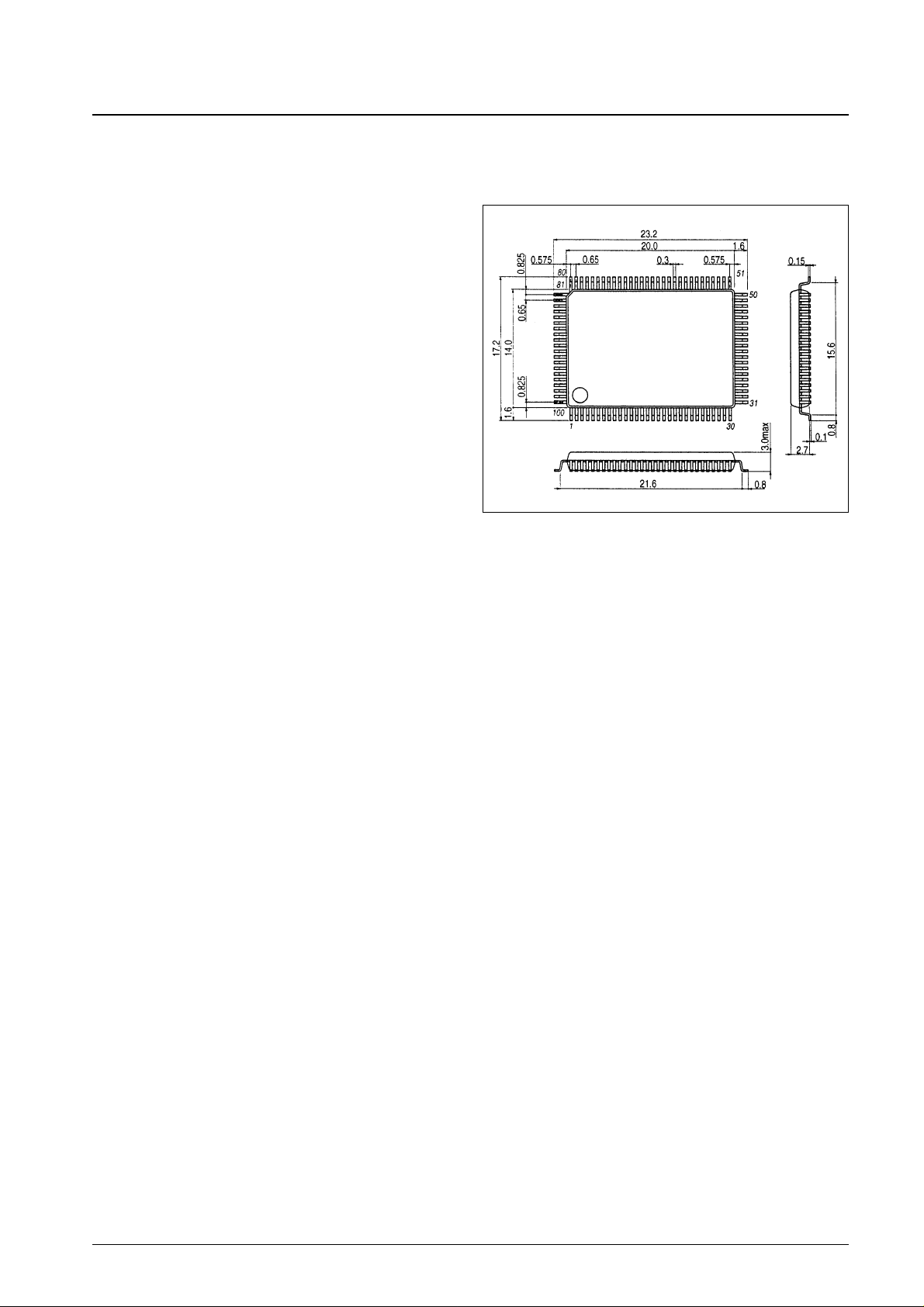
Package Dimensions
unit: mm
3151-QFP100E
No. 5931-2/14
LC723732/40/48/56/64
SANYO: QFP100E
[LC723732/40/48/56/64]
Page 3
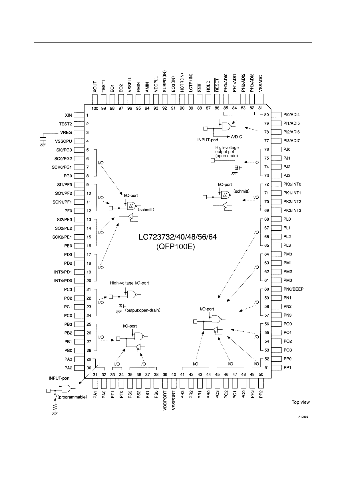
Pin Assignment
No. 5931-3/14
LC723732/40/48/56/64
Page 4
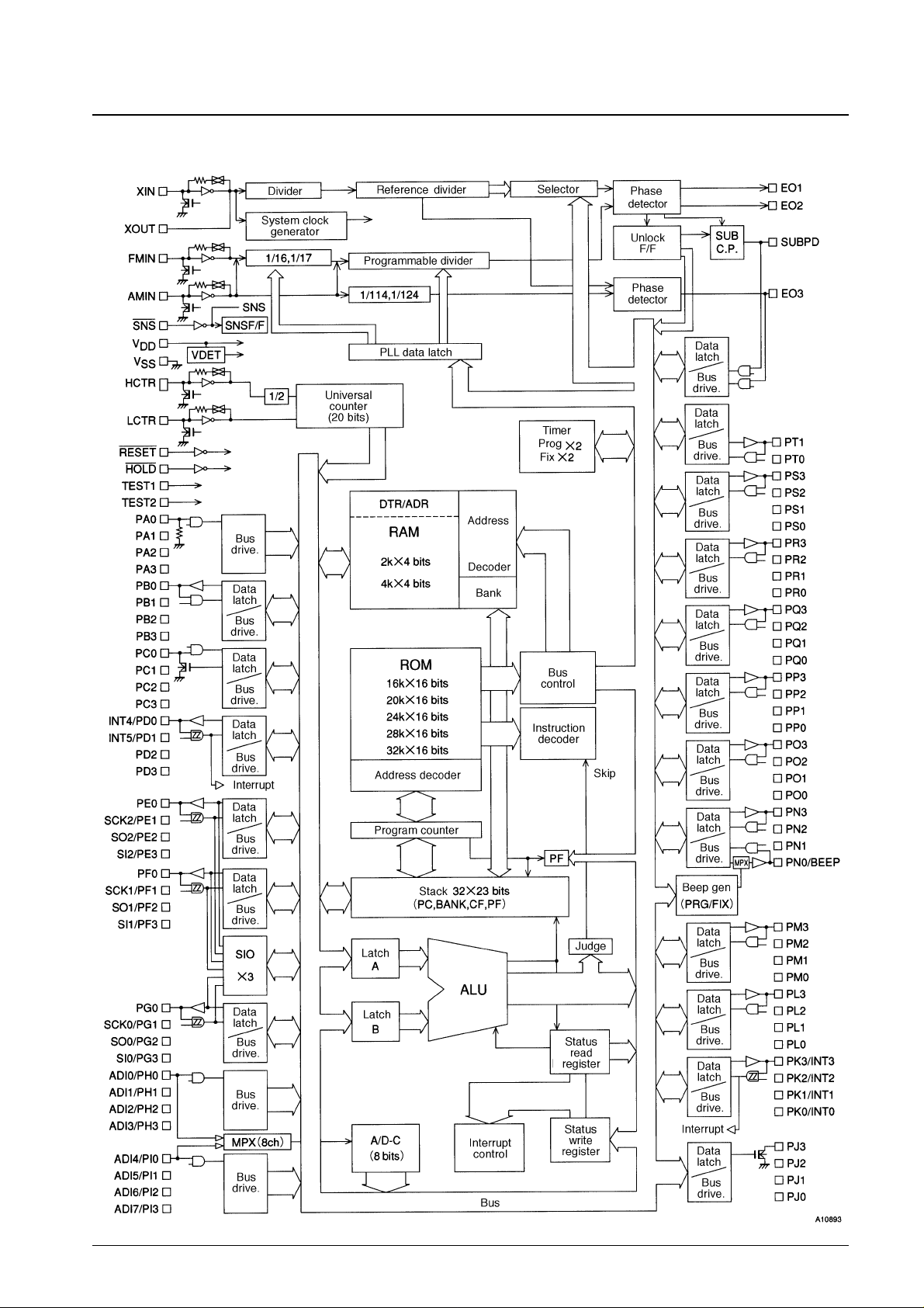
Block Diagram
No. 5931-4/14
LC723732/40/48/56/64
Page 5
No. 5931-5/14
LC723732/40/48/56/64
Parameter Symbol Conditions Ratings Unit
Maximum supply voltage V
DD
max –0.3 to +6.5 V
Input voltage
V
IN
1 PC-PORT –0.3 to +15 V
V
IN
2 All input pins other than VIN1 –0.3 to VDD+ 0.3 V
Output voltage
V
OUT
1 PC, PJ-PORT –0.3 to +15 V
V
OUT
2 All output pins other than V
OUT
1 –0.3 to VDD+ 0.3 V
I
OUT
1 PC, PJ-PORT 0 to +5 mA
Output current
I
OUT
2
PB, PD, PE, PF, PG, PK, PL, PM, PN, PO, PP, PQ, PR,
0 to +3 mA
PS, PT, PT-PORT, EO1, EO2, EO3, SUBPD
Allowable power dissipation Pd max Ta = –40 to +85°C 400 mW
Operating temperature Topg –40 to +85 °C
Storage temperature Tstg –45 to +125 °C
Specifications
Electrical Characteristics
Absolute Maximum Ratings at Ta = 25°C, VSS= 0 V
Parameter Symbol Conditions
Ratings
Unit
min typ max
V
DD
1 CPU and PLL operating 4.5 5.0 5.5 V
Supply voltage V
DD
2 CPU operating 3.5 5.5 V
V
DD
3 Memory retention 1.3 5.5 V
PB, PC, PH, PI, PL, PM, PN, PO, PP, PQ, PR,
VIH1 PS, PT-PORT, HCTR, LCTR, E03, SUBPD 0.7 V
DD
V
DD
V
(with the I/O ports set to input mode.)
Input high-level voltage
V
IH
2
PD, PE, PF, PG, PK-PORT, LCTR,
0.8 V
DD
V
DD
V
(in period measurement mode)
, HOLD, RESET
V
IH
3 SNS 2.5 V
DD
V
V
IH
4 PA-PORT 0.6 V
DD
V
DD
V
PB, PC, PH, PI, PL, PM, PN, PO, PP, PQ, PR,
VIL1 PS, PT-PORT, HCTR, LCTR, E03, SUBPD 0 0.3 V
DD
V
(with the I/O ports set to input mode.)
Input low-level voltage V
IL
2
PA, PD, PE, PF, PG, PK-PORT, LCTR
0 0.2 V
DD
V
(in period measurement mode), RESET
V
IL
3 SNS 0 1.3 V
V
IL
4 HOLD 0 0.4 V
DD
V
f
IN
1 XIN 4.0 4.5 5.0 MHz
f
IN
2 FMIN VIN2, VDD1 10 150 MHz
f
IN
3 FMIN VIN3, VDD1 10 130 MHz
f
IN
4 AMIN(H) VIN3, VDD1 2.0 40 MHz
Input frequency f
IN
5 AMIN(L) VIN3, VDD1 0.5 10 MHz
f
IN
6 HCTR VIN3, VDD1 0.4 12 MHz
f
IN
7 LCTR VIN3, VDD1 100 500 kHz
f
IN
8
LCTR(period measurement)
1 20 × 10
3
Hz
V
IH
2, VIL2, VDD1
V
IN
1 XIN 0.5 1.5 Vrms
Input amplitude V
IN
2 FMIN 0.07 1.5 Vrms
V
IN
3 FMIN, AMIN, HCTR, LCTR 0.04 1.5 Vrms
Input voltage range V
IN
4 ADI0 to ADI7 0 V
DD
V
Allowable Operating Ranges at Ta = –40 to +85°C, VDD= 3.5 to 5.5 V
Page 6

No. 5931-6/14
LC723732/40/48/56/64
Parameter Symbol Conditions
Ratings
Unit
min typ max
I
IH
1 XIN: VI= VDD= 5.0 V 2.0 5.0 15 µA
I
IH
2 FMIN, AMIN, HCTR, LCTR: VI= VDD= 5.0 V 4.0 10 30 µA
PA, PB, PC, PD, PE, PF, PG, PH, PI, PK, PL,
PM, PN, PO, PP, PQ, PR, PS, PT-PORT,
SNS, HOLD, RESET, HCTR, LCTR, E03,
Input high-level current I
IH
3 SUBPD: VI= VDD= 5.0 V 3.0 µA
(With the port PA pull-down resistors disabled,
and PB, PC, PD, PE, PF, PG, PK, PL, PM,
PN, PP, PO, PQ, PR, PS, and PT ports set to
input mode.)
I
IH
4
Port PA (pull-down resistors enabled):
50 µA
V
I
= VDD= 5.0 V
I
IL
1 XIN: VI= V
SS
2.0 5.0 15 µA
I
IL
2 FMIN, AMIN, HCTR, LCTR: VI= V
SS
4.0 10 30 µA
PA, PB, PC, PD, PE, PF, PG, PH, PI, PK, PL,
PM, PN, PO, PP, PQ, PR, PS, PT-PORT,
Input low-level current SNS, HOLD, RESET, HCTR, LCTR, E03,
I
IL
3 SUBPD: VI= V
SS
3.0 µA
(With the port PA pull-down resistors disabled,
and PB, PC, PD, PE, PF, PG, PK, PL, PM,
PN, PP, PO, PQ, PR, PS, and PT ports set to
input mode.)
Input floating voltage V
IF
Port PA (pull-down resistors enabled) 0.05 V
DD
V
Hysteresis V
H
PD, PE, PF, PG, PK-PORT, RESET,
0.1 V
DD
0.2 V
DD
V
LCTR(in period measurement mode)
VOH1
PB, PD, PE, PF, PG, PK, PL, PM, PN, PO,
VDD– 1.0 V
Output high-level voltage
PP, PQ, PR, PS, PT-PORT: I
O
= –1 mA
V
OH
2 EO1, EO2, EO3, SUBPD: IO= –500 µA VDD– 1.0 V
V
OH
3 XOUT: IO= –200 µA VDD– 1.0 V
V
OL
1
PB, PD, PE, PF, PG, PK, PL, PM, PN, PO,
1.0 V
PP, PQ, PR, PS, PT-PORT: I
O
= 1 mA
Output low-level voltage V
OL
2 E01, E02, E03, SUBPD: IO= 500 µA 1.0 V
V
OL
3 XOUT: IO= 200 µA 1.5 V
V
OL
4 PC, PJ-PORT: IO= 5 mA 2.0 V
I
OFF
1 PB, PD, PE, PF, PG, PK, PL, PM, PN, PO,
–3.0
3.0 µA
Output off leakage current
PP, PQ, PR, PS, PT-PORT
I
OFF
2 E01, E02, E03, SUBPD –100 100 nA
I
OFF
3 PC, PJ-PORT –5.0 5.0 µA
A/D conversion error ADI0 to ADI7 V
DD
1 –1.5 1.5 LSB
Rejected pulse width P
REJ
SNS 50 µsec
Power down detection voltage V
DET
2.6 3.0 3.4 V
R
PD
1
Port PA (pull-down resistors enabled):
75 100 200 kΩ
Pull-down resistance V
DD
= 5 V
R
PD
2 TEST1, TEST2 10 kΩ
I
DD
1
During normal operation (PLL operating)
20 30 mA
V
DD
1, fIN2 = 130 MHz Ta = 25°C
Halt mode (CPU operation stopped, crystal
IDD2 oscillator operating) (See figure 1.) 0.45 mA
Current drain V
DD
2, Ta = 25°C*
I
DD
3
Backup mode (crystal oscillator stopped)
5 µA
(See figure 2.) V
DD
= 5.5 V, Ta = 25°C
I
DD
4
Backup mode (crystal oscillator stopped)
1 µA
(See figure 2.) V
DD
= 2.5 V, Ta = 25°C
Electrical Characteristics in the allowable operating ranges
Note *: Twenty instruction steps are executed every millisecond. The PLL, universal counter, and other functions are stopped.
Page 7

Test Circuits
No. 5931-7/14
LC723732/40/48/56/64
Note: Ports PB through PG, and PJ through PT are all left open.
However, ports PB through PG, PK through PT, EO3, and
SUBPD are left open in output mode.
Note: Ports PA through PT are all left open.
Figure 1 IDD2 in Halt Mode Figure 2 IDD3 and IDD4 in Backup Mode
Pin Descriptions
Pin No. Symbol I/O Function Equivalent circuit
Dedicated input ports.
These ports are designed with a low threshold voltage.
The pull-down resistors for all four pins are set up together with an IOS1 instruction.
The pull-down resistors cannot be set individually.
Input is disabled in backup mode.
32
31
30
29
PA0
PA1
PA2
PA3
I
General-purpose I/O ports
The mode (input or output) is set using the IOS2 instruction.
Input is disabled and the pins go to the high-impedance state in backup mode.
These ports are set up as general-purpose input ports after a power on reset.
28
27
26
25
PB0
PB1
PB2
PB3
I/O
General-purpose I/O ports (high-voltage input and output)
The mode (input or output) is set using the IOS2 instruction.
External pull-up resistors are required since the output circuits are open drain
circuits.
Input is disabled and the pins go to the high-impedance state in backup mode.
These ports are set up as general-purpose input ports after a power on reset.
24
23
22
21
PC0
PC1
PC2
PC3
I/O
General-purpose I/O and external interrupt shared function ports
The input formats are Schmitt inputs.
The external interrupt function is enabled when the external interrupt enable flag is
set.
• When used as general-purpose I/O ports:
The mode (input or output) is set in 1-bit units using the IOS2 instruction.
• When used as external interrupt pins:
The external interrupt functions are enabled by setting the corresponding external
interrupt enable flag (INT4EN or INT5EN). Here, the pins must be set to input
mode in advance.
Input is disabled and the pins go to the high-impedance state in backup mode.
These ports are set up as general-purpose input ports after a power on reset.
20
19
18
17
PD0/INT4
PD1/INT5
PD2
PD3
I/O
Continued on next page.
Page 8

No. 5931-8/14
LC723732/40/48/56/64
Continued from preceding page.
Pin No. Symbol I/O Function Equivalent circuit
General-purpose I/O ports with shared functions as serial I/O ports
The input formats are Schmitt inputs. The PE1/SCK2 and PE2/SO2 pins can be
switched to function as open drain outputs.
The IOS1 instruction is used to switch between the general-purpose I/O port and
serial I/O port functions.
• When used as general-purpose I/O ports:
The pins are set to the general-purpose I/O port function using the IOS1
instruction.
The mode (input or output) is set in 1-bit units using the IOS1 instruction.
• When used as serial I/O ports:
The pins are set to the serial I/O port function using the IOS1 instruction.
[Pin states when set to the serial I/O port function]
PE0, PF0, PG0 ... General-purpose I/O
PE1, PF1, PG1 ... SCK input or output
PE2, PF2, PG2 ... SO output
PE3, PF3, PG3 ... SI input
The PE1/SCK2 and PE2/SO2 pins can be switched to function as open drain
outputs with the IOS2 instruction. When using this circuit type, the external pull-up
resistors must be connected to the same power supply as that used by the IC.
Input is disabled and the pins go to the high-impedance state in backup mode.
These ports are set up as general-purpose input ports after a power on reset.
16
15
14
13
12
11
10
9
8
7
6
5
PE0
PE1/SCK2
PE2/S02
PE3/SI2
PF0
PF1/SCK1
PF2/S01
PF3/SI1
PG0
PG1/SCK0
PG2/S00
PG3/SI0
I/O
Connections for a 4.5-MHz crystal oscillator element
1
100
XIN
XOUT
I
O
Main charge pump outputs
These pins output a high level when the frequency of the local oscillator divided by n
is higher than that of the reference frequency, and they output a low level when that
frequency is lower. They go to the high-impedance state when the frequencies
match.
These pins go to the high-impedance state in backup mode, after a power on reset,
and in the PLL stopped state.
98
97
E01
E02
O
Power supply connections
The V
DD
PORT and VSSPORT pins mainly supply power for the peripheral I/O blocks
and the regulator.
The V
DD
PLL and VSSPLL pins mainly for the PLL circuits.
The V
SS
CPU pin is mainly used by the CPU block.
The V
SS
ADC pin is mainly used by the A/D converter block.
Since all the V
DD
and VSSpins are independent, all must be connected to the same
power supply.
39
93
4
40
81
96
V
DD
PORT
V
DD
PLL
V
SS
CPU
V
SS
PORT
V
SS
ADC
V
SS
PLL
—
Internal low voltage output
Connect a bypass capacitor to this pin.
3
V
REG
O
FM VCO (local oscillator) input
This pin is selected with CW1 in the PLL instruction.
The signal input to this pin must be capacitor coupled.
Input is disabled in backup mode, after a power on reset, and in the PLL stopped
state.
95
FM
IN
I
AM VCO (local oscillator) input
This pin is selected and the band set with CW1 (b1, b0) in the PLL instruction.
The signal input to this pin must be capacitor coupled.
Input is disabled in backup mode, after a power on reset, and in the PLL stopped
state.
94
AM
IN
I
b1 b0 Band
1 0 2 to 40 MHz (SW)
1 1 0.5 to 10 MHz (MW, LW)
Continued on next page.
Page 9

No. 5931-9/14
LC723732/40/48/56/64
Continued from preceding page.
Pin No. Symbol I/O Function Equivalent circuit
Sub-charge pump output and general-purpose input shared function port
The IOS2 instruction is used for switching between the sub-charge pump output and
general-purpose input functions.
• When used as the sub-charge pump output:
The sub-charge pump output function is set up with the IOS2 instruction.
A high-speed locking circuit can be formed by using this pin in conjunction with the
main charge pump.
The sub-charge pump is controlled using the DZC instruction.
• When used as a general-purpose input:
The general-purpose input function is set up with the IOS2 instruction.
Data is read from the port using the INR instruction.
This pin goes to the high-impedance state in backup mode, after a power on reset,
and in the PLL stopped state.
92 SUBPD I/O
Second PLL charge pump output and general-purpose input shared function port
The IOS2 instruction is used for switching between the second PLL charge pump
output and general-purpose input functions.
• When used as a charge pump output:
The charge pump output function is set up with the IOS2 instruction.
This pin outputs a low level when the frequency of the local oscillator divided by n
is higher than that of the reference frequency, and it outputs a high level when that
frequency is lower. It goes to the high-impedance state when the frequencies
match. (Note that the logic of this pin is inverted from that of the EO1 and EO2
pins.)
• When used as a general-purpose input:
The general-purpose input function is set up with the IOS2 instruction.
Data is read from the port using the INR instruction.
This pin goes to the high-impedance state in backup mode, after a power on reset,
and in the PLL stopped state.
91 E03 I/O
Universal counter and general-purpose input shared function input port
The IOS1 instruction is used for switching between the universal counter and
general-purpose input functions.
• When used for frequency measurement:
The universal counter function is set up with the IOS1 instruction.
The counter is controlled using the UCS and UCC instructions.
Since this pin functions as an AC amplifier in this mode, the input signal must be
input with capacitor coupling.
• When used as a general-purpose input pin:
The general-purpose input function is set up with the IOS1 instruction.
Data is read from the port using the INR (b0) instruction.
Input is disabled in backup mode. (The input pin will be pulled down.) The universal
counter function is selected after a power on reset.
90 HCTR I
Universal counter (frequency or period measurement) and general-purpose input
shared function input port
The IOS1 instruction is used for switching between the universal counter and
general-purpose input functions.
• When used for frequency measurement:
The universal counter function is set up with the IOS1 instruction.
Set up LCTR frequency measurement mode with the UCS instruction, and control
operation with the UCC instruction. Since this pin functions as an AC amplifier in
this mode, the input signal must be input with capacitor coupling.
• When used for period measurement:
The universal counter function is set up with the IOS1 instruction.
Set up LCTR frequency measurement mode with the UCS instruction, and control
operation with the UCC instruction. Since the bias feedback resistor is
disconnected in this mode, the input signal must be input with DC coupling.
• When used as a general-purpose input pin:
The general-purpose input port function is set up with the IOS1 instruction.
Data is read from the port using the INR (b1) instruction.
Input is disabled in backup mode. (The input pin will be pulled down.)
The universal counter function (HCTR frequency measurement mode) is selected
after a power on reset.
89 LCTR I
b3 b2 Operation
0 0 High impedance
0 1 Only operates when the PLL is unlocked (450 kHz)
1 0 Only operates when the PLL is unlocked (900 kHz)
1 1 Normal operation
Continued on next page.
Page 10

No. 5931-10/14
LC723732/40/48/56/64
Continued from preceding page.
Pin No. Symbol I/O Function Equivalent circuit
Voltage sense and general-purpose input shared function port
This input circuit is designed with a low input threshold voltage.
• When used as a voltage sense input:
This pin is used to test for power failures on the return from backup mode.
Application can test this condition using the internal SNS flip-flop. The SNS flip-flop
can be tested with the TST instruction.
(This usage requires external components (capacitors and resistors). See the
sample application circuit in the user's manual.)
• When used as a general-purpose input port:
When used as a general-purpose input port the pin state can be tested with the
TST instruction.
Unlike the other input ports, input to this pin is not disabled in backup mode and after
a power on reset. As a result, through currents must be taken into account when
designing applications that use this pin as a general-purpose input.
88 SNS I
Power supply monitor (with interrupt function)
This pin is designed with a high input threshold voltage.
This pin is normally connected to the ACC line and used for power off detection.
When a power off state is detected, the HOLDON flag and the hold interrupt request
flag will be set. To enter backup mode, execute a CKSTP instruction when the HOLD
pin is low. Set this pin high to clear backup mode.
87 HOLD I
System reset pin
When the CPU is operating or in halt mode, the system is reset when this pin is held
low for at least one machine cycle. Execution starts with the PC pointing to location
0. At this time the SNS flip-flop is set. A low level must be applied for at least 50 ms
when power is first applied.
86 RESET I
General-purpose input and A/D converter input shared function ports
The IOS1 instruction is used to switch between the general-purpose input and the
A/D converter input functions.
• When used as a general-purpose input ports:
The general-purpose input port function is set up with the IOS1 instruction. (In bit
units)
• When used as A/D converter input pins:
The A/D converter input port function is set up with the IOS1 instruction. (In bit
units)
The pin whose voltage is to be converted is specified with the IOS1 instruction, and
the conversion is started with the UCC instruction.
Note: Since input is disabled for ports specified for the ADI function, executing an
input instruction for such a port will always return a low level.
Input is disabled in backup mode.
These ports are set up as general-purpose input ports after a power on reset.
85
84
83
82
81
80
79
78
PH0/ADI0
PH1/ADI1
PH2/ADI2
PH3/ADI3
PI0/ADI4
PI1/ADI5
PI2/ADI6
PI3/ADI7
I
General-purpose output ports
Since these are open-drain output circuits, external pull-up resistors are required.
The internal transistors are turned off (resulting in a high-level output) in backup
mode and after a power on reset.
76
75
74
73
PJ0
PJ1
PJ2
PJ3
O
General-purpose I/O and external interrupt shared function ports
The input formats are Schmitt inputs.
The external interrupt function is enabled when the external interrupt enable flag is
set.
• When used as general-purpose I/O ports:
The mode (input or output) is set in 1-bit units using the IOS1 instruction.
• When used as external interrupt pins:
The external interrupt functions are enabled by setting the corresponding external
interrupt enable flag (INT0EN through INT3EN). Here, the pins must be set to input
mode in advance.
Input is disabled and the pins go to the high-impedance state in backup mode.
These ports are set up as general-purpose input ports after a power on reset.
72
71
70
69
PK0/INT0
PK1/INT1
PK2/INT2
PK3/INT3
I/O
Continued on next page.
Page 11

No. 5931-11/14
LC723732/40/48/56/64
Continued from preceding page.
Pin No. Symbol I/O Function Equivalent circuit
General-purpose I/O ports
The mode is switched between input and output with the IOS instruction.
Input is disabled and the pins go to the high-impedance state in backup mode.
These ports are set up as general-purpose input ports after a power on reset.
68 to 61
PL0 to 3
PN0 to 3
I/O
General-purpose I/O port and beep tone output shared function ports
The IOS2 instruction is used to switch between the general-purpose I/O port and the
beep tone output functions.
• When used as a general-purpose input ports:
The general-purpose I/O port function is set up with the IOS2 instruction.
(Pins PN1 through PN3 are general-purpose I/O pins.)
• When used as the beep tone output pin:
The beep tone output function is set up with the IOS2 instruction.
The frequency is set with the BEEP instruction.
When this pin is used as the beep tone output pin, executing an output instruction
for this pin only sets the internal latch and has no influence on the output.
Input is disabled and the pins go to the high-impedance state in backup mode.
These ports are set up as general-purpose input ports after a power on reset.
60
59
58
57
PN0/BEEP
PN1
PN2
PN3
I/O
General-purpose I/O ports
The mode is switched between input and output with the IOS instruction.
Input is disabled and the pins go to the high-impedance state in backup mode.
These ports are set up as general-purpose input ports after a power on reset.
56 to 49
P00 to 3
PP0 to 3
I/O
General-purpose I/O ports
The mode is switched between input and output with the IOS instruction, and data is
input with the INR instruction and output with the OUTR instruction.
The SPB, RPB, TPT, and TPF instruction cannot be used with these ports.
Input is disabled and the pins go to the high-impedance state in backup mode.
These ports are set up as general-purpose input ports after a power on reset.
48 to 41
38 to 33
PQ0 to 3
PR0 to 3
PS0 to 3
PT0 to 1
I/O
IC test pins
These pins must be tied to ground.
99
2
TEST1
TEST2
Page 12

LC723700 Instruction Set
Abbreviations
ADDR: Program memory address
b: Borrow
c: Carry
DH: Data memory address High (Row address) [2 bits]
DL: Data memory address Low(Column address) [4 bits]
I: Immediate data [4 bits]
M: Data memory address
N: Bit position [4 bits]
M
ADR
: M specified by address register
ROM
ADR
: Program memory data specified by address register
P1n, P2n: Port number [4 bits]
PW1n, PW2n: Port control word number [4 bits]
PEn: Peripheral register number [4 bits]
SR: ADR/DTR
ADR: Address register
DTR: Data register
r: General register (One of the address from 00H to 0FH of BANK0)
SWR: Status write register
SRR: Status read register
( ), [ ]: Contents of register or memory
M(DH, DL): Data memory specified by DH, DL
No. 5931-12/14
LC723732/40/48/56/64
Mnemonic
Operand
Function Operations function
Instruction format
1st 2nd
AD r M Add M to r r ←(r) + (M) 0 1 0 0 0 0 DH DL r
ADS r M ADD M to r, then skip if carry r ← (r) + (M), skip carry 0 1 0 0 0 1 DH DL r
AC r M Add M to r with carry r ← (r) + (M) + C 0 1 0 0 1 0 DH DL r
ACS r M Add M to r with carry, then skip if carry r ← (r) + (M) + C skip if carry 0 1 0 0 1 1 DH DL r
AI M I Add I to M M ← (M) + I 0 1 0 1 0 0 DH DL I
AIS M I Add I to M, then skip if carry M ← (M) + I, skip if carry 0 1 0 1 0 1 DH DL I
AIC M I Add I to M with carry M ← (M) + I + C 0 1 0 1 1 0 DH DL I
AICS M I Add I to M with carry, then skip if carry M ← (M) + I + C, skip if carry 0 1 0 1 1 1 DH DL I
SU r M Subtract M from r r ← (r) – (M) 0 1 1 0 0 0 DH DL r
SUS r M Subtract M from r, then skip if borrow r ← (r) – (M), skip if borrow 0 1 1 0 0 1 DH DL r
SB r M Subtract M from r with borrow r ← (r) – (M) – b 0 1 1 0 1 0 DH DL r
SBS r M
Subtract M from r with borrow,
r ← (r) – (M) –b, skip if borrow 0 1 1 0 1 1 DH DL r
then skip if borrow
SI M I Subtract I from M M ← (M) – I 0 1 1 1 0 0 DH DL I
SIS M I Subtract I from M, then skip if borrow M ← (M) – I, skip if borrow 0 1 1 1 0 1 DH DL I
SIB M I Subtract I from M with borrow M ←(M) – I – b 0 1 1 1 1 0 DH DL I
SIBS M I
Subtract I from M with borrow,
M ← (M) – I –b, skip if borrow 0 1 1 1 1 1 DH DL I
then skip if borrw
SEQ r M Skip if r equal to M (r) – (M), skip if zero 0 0 0 1 0 0 DH DL r
SEQI M I Skip if M equal to I (M) – I, skip if zero 0 0 0 1 0 1 DH DL I
SNEI M I Skip if M not equal to I (M) – I, skip if not zero 0 0 0 0 0 1 DH DL I
SGE r M Skip if r is greater than or equal to M (r) – (M), skip if not borrow 0 0 0 1 1 0 DH DL r
SLE r M Skip if r is less than M (r) – M, skip if borrow 0 0 0 0 1 0 DH DL r
SGEI M I Skip if M is greater than or equal to I (M) – I, skip if not borrow 0 0 0 1 1 1 DH DL I
SLEI M I Skip if M is less than I (M) – I, skip if borrow 0 0 0 0 1 1 DH DL I
Subtraction instructionsComparison instructions Addition instructions
Instruction
group
f e d c b a 9 8 7 6 5 4 3 2 1 0
Continued on next page.
Page 13

No. 5931-13/14
LC723732/40/48/56/64
Continued from preceding page.
Mnemonic
Operand
Function Operations function
Instruction format
1st 2nd
AND r M AND M with r r ← (r) AND (M) 0 0 1 0 0 0 DH DL r
ANDI M I AND I with M M ← (M) AND I 0 0 1 0 0 1 DH DL I
OR r M OR M with r r ← (r) OR (M) 0 0 1 0 1 0 DH DL r
ORI M I OR I with M M ←(M) OR I 0 0 1 0 1 1 DH DL I
EXL r M Exclusive OR M with r r ← (r) XOR (M) 0 0 1 1 0 0 DH DL r
EXLI M I Exclusive OR M with M M ← (M) XOR I 0 0 1 1 0 1 DH DL I
SHMR M Shift M right with carry 1 1 1 1 1 1 1 1 1 0 DH DL
LD r M Load M to r r ← (M) 1 1 0 1 0 0 DH DL r
ST M r Strore r to M M ← (r) 1 1 0 1 0 1 DH DL r
LDA r Load M specified by ADR to r r ← (M
ADR
) 1 1 1 1 1 0 0 1 1 1 0 0 r
STA r Store r to M specified by ADR M
ADR
← (r) 1 1 1 1 1 0 0 1 1 1 0 1 r
MVRD r M
Move M to destination M referring to r in
[DH, rn] ← (M) 1 1 0 1 1 0 DH DL r
the same row
MVRS M r
Move source M referring to r to M in the
M ← (DH, rn) 1 1 0 1 1 1 DH DL r
same row
MVSR M1 M2 Move M to M in the same row [DH, DL1] ← [DH, DL2] 1 1 1 0 0 0 DH DL DL2
MVI M I Move I to M M ← I 1 1 1 0 0 1 DH DL I
TMT M N
Test M bits, then skip if all bits specified
if M(N) = all 1, then skip 1 1 1 1 0 0 DH DL N
are true
TMF M N
Test M bits, then skip if all bits specified
if M(N) = all 0, then skip 1 1 1 1 0 1 DH DL N
are false
JMP ADDR Jump to the address PC ← ADDR 1 0 ADDR(14 bits)
JMPA Jump to the address specified by ADR PC ← (ADR) 0 0 0 0 0 0 0 0 1 1 1 0
JMPR ADDR Jump to the relative address PC ← (PC) + 1 + ADDR 1 1 1 1 1 0 1 0 ADDR (8 bits)
CAL ADDR Call subroutine
PC ← ADDR
1 1 0 0 ADDR(12 bits)
Stack ← (PC) + 1
CALA Call subroutine specified by ADR
PC ← (ADR)
0 0 0 0 0 0 0 0 1 1 1 1
Stack ← (PC) + 1
RT Return from subroutine PC ← Stack 0 0 0 0 0 0 0 0 1 0 0 0
RTS Return from subroutine and skip PC ← Stack + 1 0 0 0 0 0 0 0 0 1 0 1 0
RTB Return from subroutine with BANK data
PC ← Stack,
1 1 1 1 1 1 1 1 1 1 0 0
BANK ← Stack
RTBS
Return from subroutine with BANK data PC ← Stack + 1,
1 1 1 1 1 1 1 1 1 1 0 1
and skip BANK ← Stack
PC ← Stack,
RTI Return from interrupt
BANK ← Stack,
0 0 0 0 0 0 0 0 1 0 0 1
CARRY ← Stack
PAGE ← Stack
SS SWR N Set status register (Status W-reg)N ← 1 1 1 1 1 1 1 1 1 0 0 SWR N
RS SWR N Reset status register (Status W-reg)N ← 0 1 1 1 1 1 1 1 1 0 1 SWR N
TST SRR N Test status register true
if (Status R-reg)N = all1, then skip
1 1 1 1 1 0 0 0 0 SRR N
TSF SRR N Test status register false
if (Status R-reg)N = all0, then skip
1 1 1 1 1 0 0 0 1 SRR N
PLL M Load M to PLL register PLL reg ← PLL data 1 1 1 1 1 0 0 1 0 1 DH DL
PUT PEn Put data of DTR to perifheral register PEn ← (DTR) 1 1 1 1 1 0 0 1 1 0 1 0 PEn
GET PEn Get peripheral data to DTR DTR ← (PEn) 1 1 1 1 1 0 0 1 1 0 1 1 PEn
SIO I1 I2 Serial I/O control SIO reg ← I1, I2 0 0 0 0 0 0 0 1 I1 I2
UCS I Set I to UCCW1 UCCW1 ← I 0 0 0 0 0 0 0 0 0 0 0 1 I
UCC I Set I to UCCW2 UCCW2 ← I 0 0 0 0 0 0 0 0 0 0 1 0 I
BEEP I Beep control BEEP reg ← I 0 0 0 0 0 0 0 0 0 1 1 0 I
DZC I Dead zone control DZC reg ← I 0 0 0 0 0 0 0 0 1 0 1 1 I
TMS I Set timer register Timer reg ← I 0 0 0 0 0 0 0 0 1 1 0 0 I
IOS1 PW1n N Set port control word1 IOS1 reg PW1n ← N 1 1 1 1 1 1 1 0 PW1n N
IOS2 PW2n N Set port control word2 IOS2 reg PW2n ← N 1 1 1 1 1 0 1 1 PW2n N
Logical operation
instructions
Transfer instructions
Bit test
instructions
Jump and subroutine instructions
Internal register
transfer instructions
Hardware control instructions
Status register
instructions
Instruction
group
f e d c b a 9 8 7 6 5 4 3 2 1 0
carry
(M)
Continued on next page.
Page 14

PS No. 5931-14/14
LC723732/40/48/56/64
This catalog provides information as of June, 1998. Specifications and information herein are subject to change
without notice.
■ No products described or contained herein are intended for use in surgical implants, life-support systems, aerospace
equipment, nuclear power control systems, vehicles, disaster/crime-prevention equipment and the like, the failure of
which may directly or indirectly cause injury, death or property loss.
■ Anyone purchasing any products described or contained herein for an above-mentioned use shall:
➀ Accept full responsibility and indemnify and defend SANYO ELECTRIC CO., LTD., its affiliates, subsidiaries and
distributors and all their officers and employees, jointly and severally, against any and all claims and litigation and all
damages, cost and expenses associated with such use:
➁ Not impose any responsibility for any fault or negligence which may be cited in any such claim or litigation on
SANYO ELECTRIC CO., LTD., its affiliates, subsidiaries and distributors or any of their officers and employees
jointly or severally.
■ Information (including circuit diagrams and circuit parameters) herein is for example only; it is not guaranteed for
volume production. SANYO believes information herein is accurate and reliable, but no guarantees are made or implied
regarding its use or any infringements of intellectual property rights or other rights of third parties.
Continued from preceding page.
Mnemonic
Operand
Function Operations function
Instruction format
1st 2nd
IN M P1n Input port1 data to M M ← (P1n) 1 1 1 0 1 0 DH DL P1n
OUT M P1n Output contents of M to port 1 P1n ← M 1 1 1 0 1 1 DH DL P1n
INR M P2n Input port 2 data to M M ← (P2n) 0 0 1 1 1 0 DH DL P2n
OUTR M P2n Output contents of M to port 2 P2n ←(M) 0 0 1 1 1 1 DH DL P2n
SPB P1n N Set port 1 bits (P1n)N ← 1 0 0 0 0 0 0 1 0 P1n N
RPB P1n N Reset port 1 bits (P1n)N ← 0 0 0 0 0 0 0 1 1 P1n N
TPT P1n N
Test port 1 bits, then skip if all bits
if (P1n)N = all 1, then skip 1 1 1 1 1 1 0 0 P1n N
specified are true
TPF P1n N
Test port 1 bits, then skip if all bits
if (P1n)N = all 0, then skip 1 1 1 1 1 1 0 1 P1n N
specified are false
BANK I Select Bank BANK ← I 1 1 1 1 1 0 0 1 0 0 I
MVTL
Move program memory data specified by
DTR ← (ROM
ADR
)
0 0 0 0 0 0 0 0 0 0 1 1
ADR to DTR
PUSH SR Move ADR/DTR to stack Stack ← (ADR/DTR) 1 1 1 1 1 0 0 1 1 0 0 0 SR
POP SR Move stack to ADR/DTR ADR/DTR ← Stack 1 1 1 1 1 0 0 1 1 0 0 1 SR
PAGE I Set page flag PAGE flag ← I 0 0 0 0 0 0 0 0 0 1 1 1 I
HALT I Halt mode control
HALT reg ← I,
0 0 0 0 0 0 0 0 0 1 0 0 I
then CPU clock stop
CKSTP Clock stop Stop xtal OSC if HOLD = 0 0 0 0 0 0 0 0 0 0 1 0 1
NOP No operation No operation 0 0 0 0 0 0 0 0 0 0 0 0
I/O instructions
Bank switching
instructions
Table reference
instructions
Stack manipulation
instructions
Other instructions
Instruction
group
f e d c b a 9 8 7 6 5 4 3 2 1 0
 Loading...